

A Flexible System-on-Chip Field-Programmable Gate Array Architecture for Prototyping Experimental Global Navigation Satellite System Receivers

Abstract
:1. Introduction
1.1. Motivation
1.2. Contributions
1.3. Organization of the Paper
2. Literature Review

| Year | CPU | CPU, GPU | FPGA, DSP | FPGA | CPU, FPGA | CPU, FPGA, GPU | SoC- FPGA |
|---|---|---|---|---|---|---|---|
| 1997 | [25] | ||||||
| 2003 | [26] | ||||||
| 2004 | [33] | [34] | |||||
| 2006 | [39] | ||||||
| 2008 | [31] | ||||||
| 2009 | [27] | ||||||
| 2010 | [28] | [32] | [40] | ||||
| 2011 | [11] | [41,44,45] | |||||
| 2012 | [42,43] | ||||||
| 2013 | [46] | ||||||
| 2014 | [35,36] | ||||||
| 2015 | [29] | ||||||
| 2018 | [30] | ||||||
| 2019 | [37] | [48] | |||||
| 2020 | [47] | ||||||
| 2021 | [49] | ||||||
| 2022 | [38] | [50] |
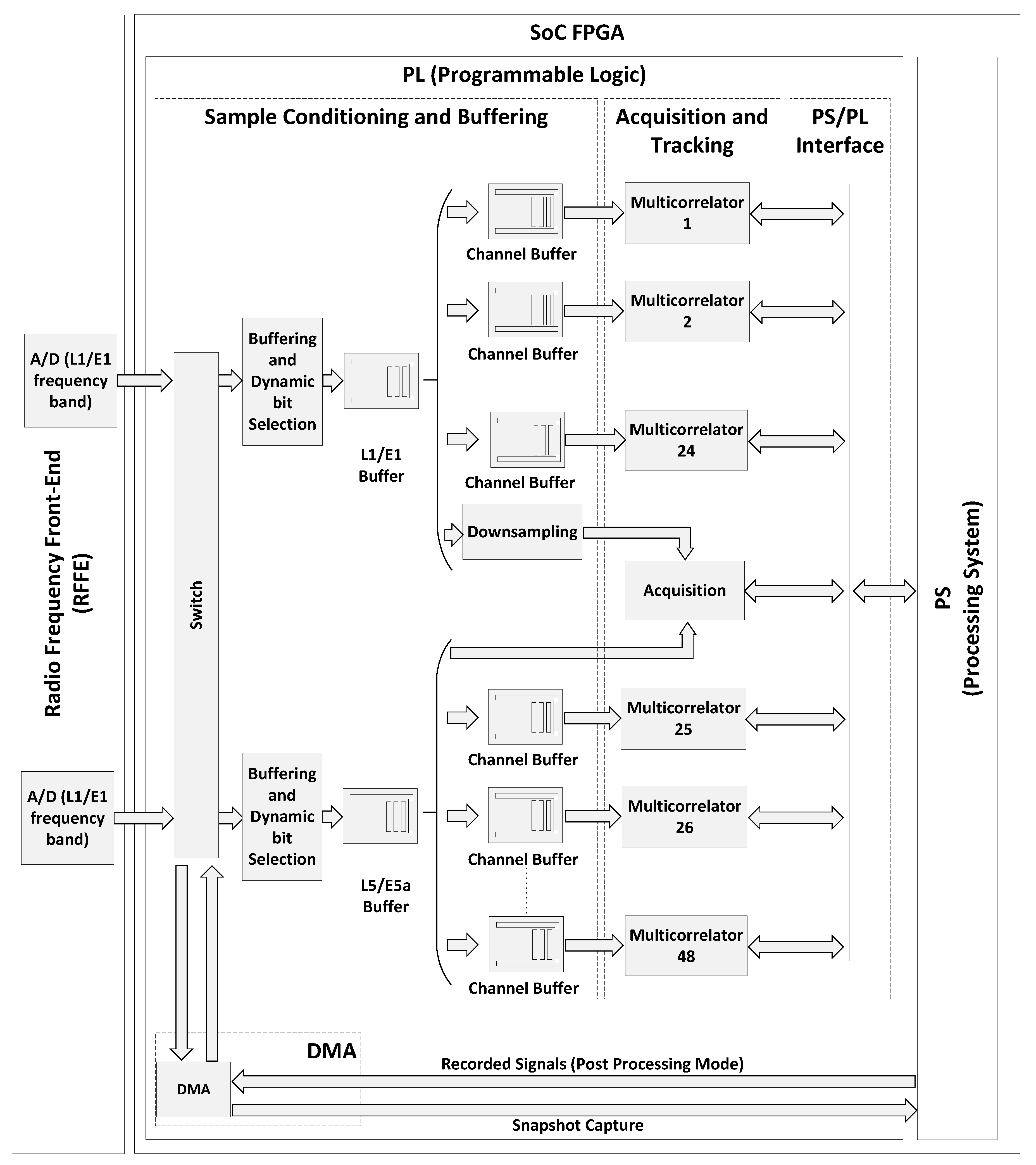
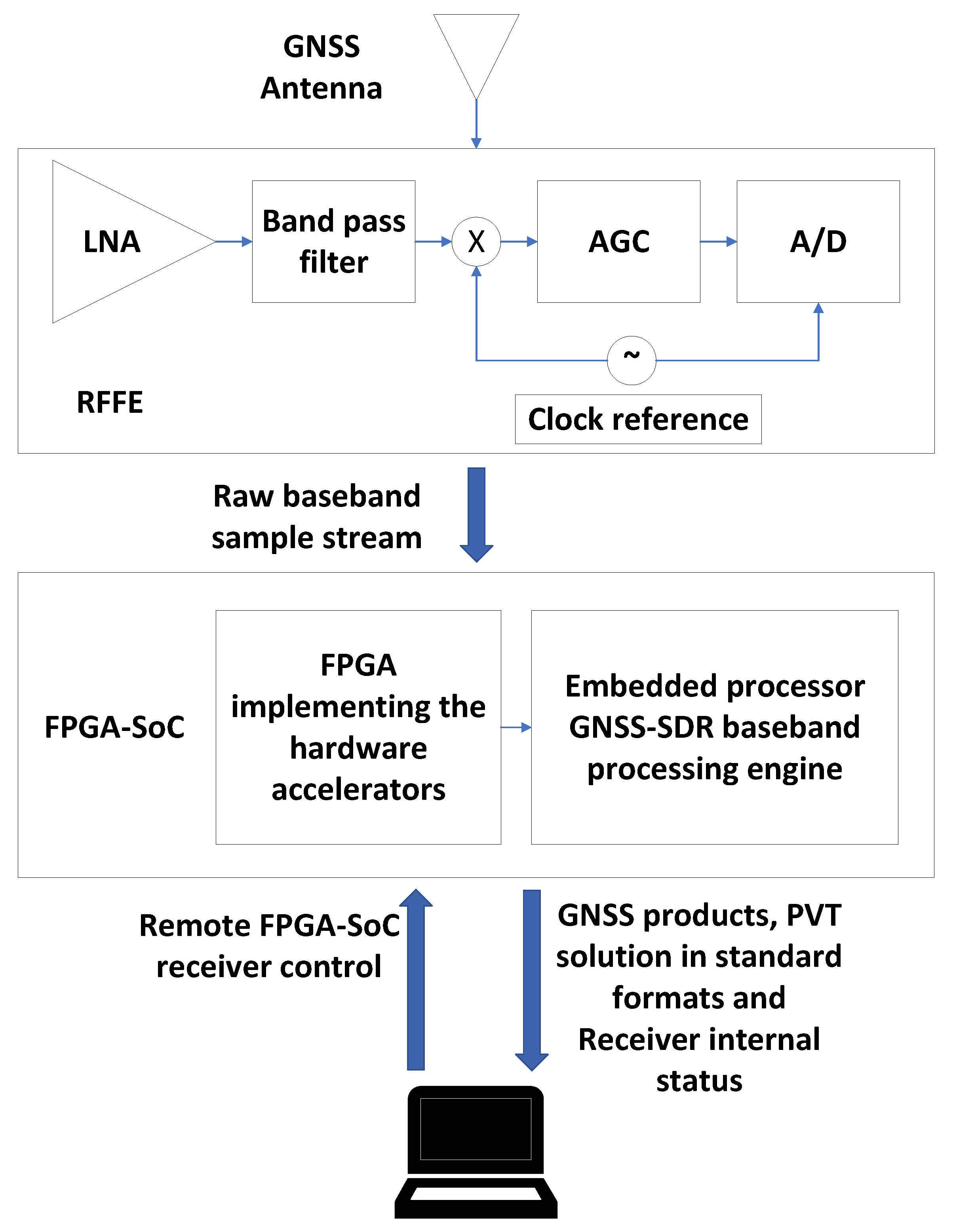
3. System Design
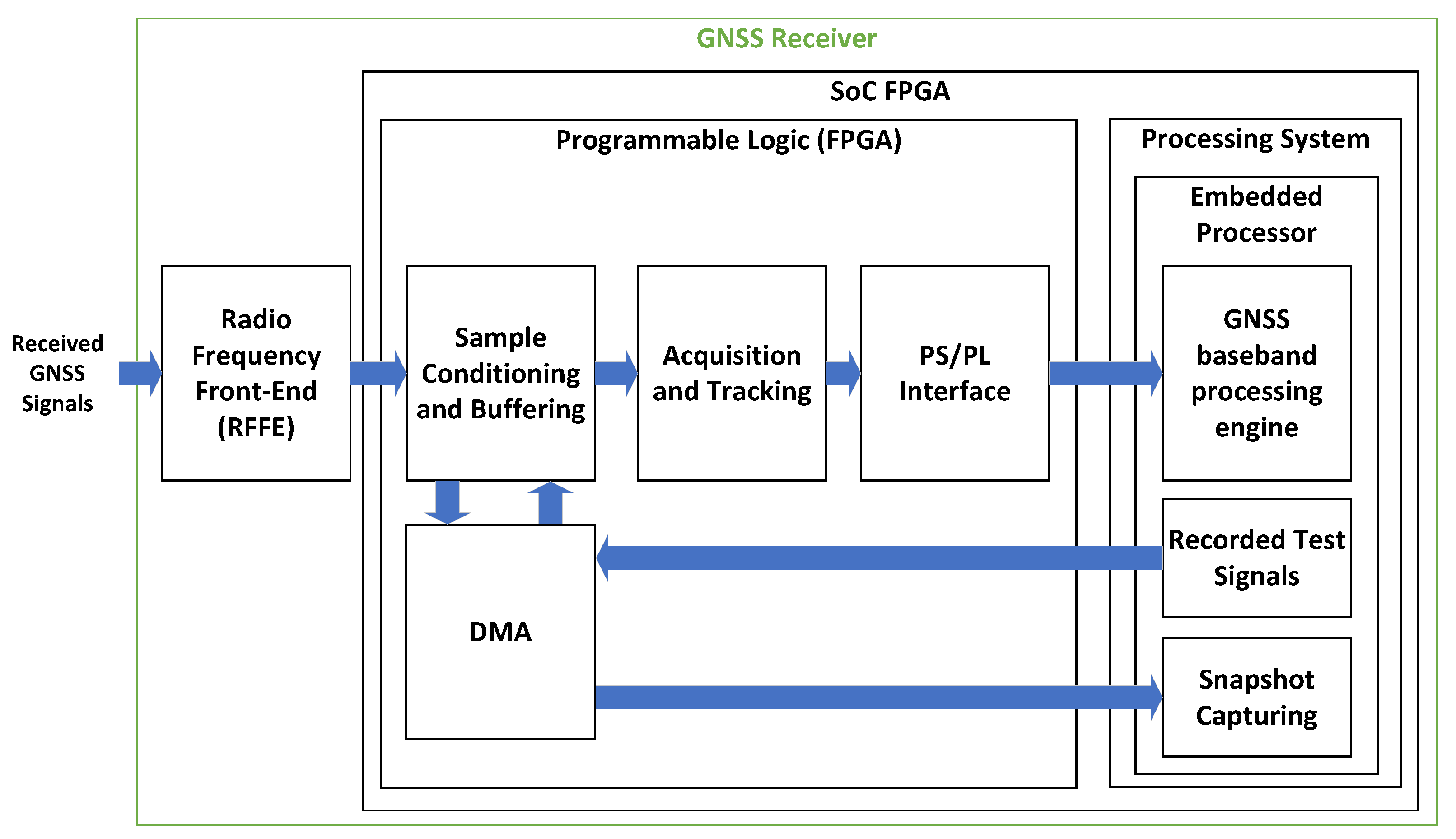
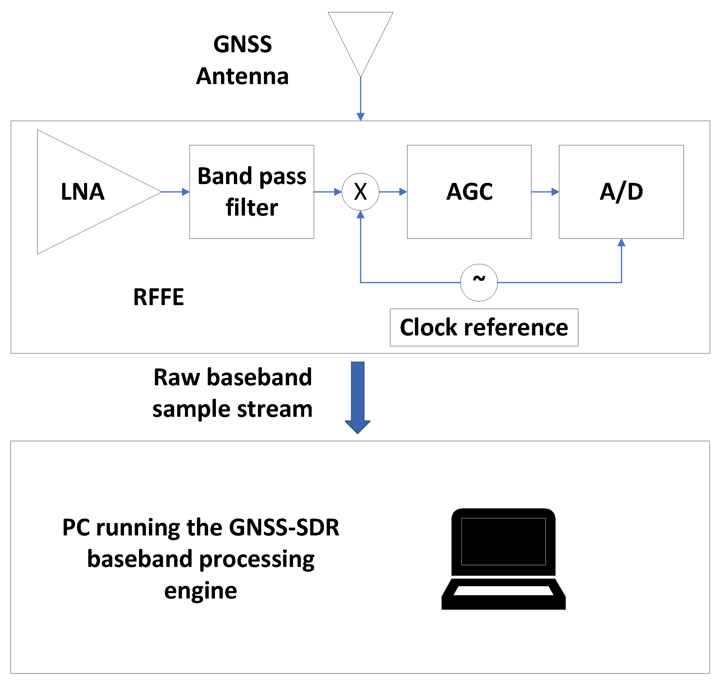
3.1. Overview


- 1.
- Sample Conditioning and Buffering: The sample conditioning and buffering block receives the samples coming from the RFFE and implements sample buffering and clock conversion between the front-end interface and the FPGA hardware accelerators. The sample conditioning and buffering block also implements a bit selector, used to dynamically requantize the GNSS signals to map the dynamic range of the incoming samples to the dynamic range of the acquisition and tracking hardware multicorrelators.
- 2.
- Acquisition and Tracking: The FPGA incorporates hardware accelerators for the algorithms with the highest computational cost: the acquisition and tracking multicorrelators [13]. The most computationally expensive algorithms are the signal processing stages that process the digitized signals at the sampling rate. However, it is also possible to offload any other processor intensive algorithms to the FPGA.
- 3.
- DMA: the FPGA implements a bi-directional direct memory access (DMA). The DMA can be used to run the receiver in post-processing mode using recorded GNSS files, to record the received GNSS signals into files, to capture snapshots, or to send the received GNSS signals to an external device in real time.
- 4.
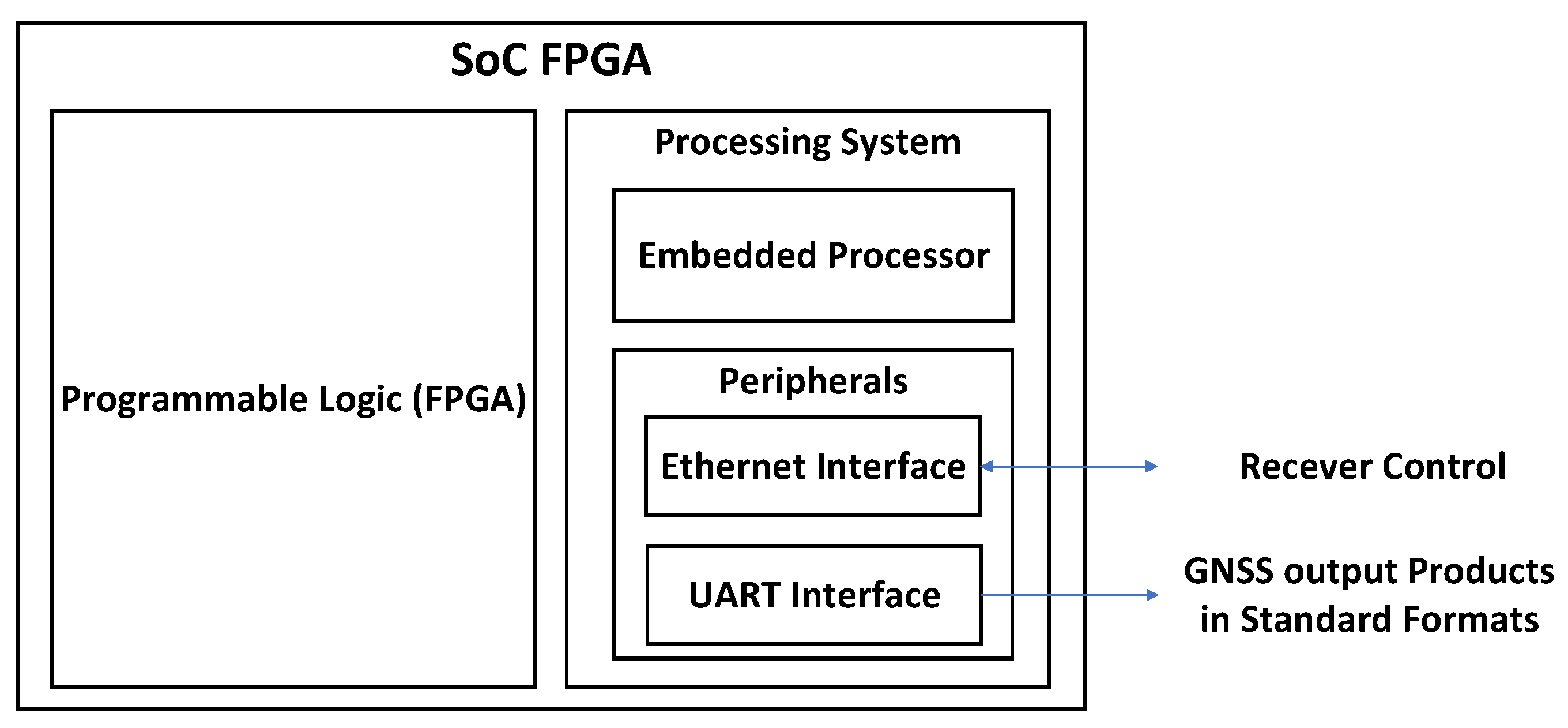
- PS/PL Interface: Interface between the FPGA and the processing system. This interface is implemented using the Advanced Microcontroller Bus Architecture (AMBA) Advanced eXtensible Interface (AXI4) memory-mapped bus. Most SoC-FPGAs support the AMBA architecture. The GNSS baseband engine controls the execution of the acquisition and tracking multicorrelators using a set of memory-mapped registers, and a set of interrupts going from the FPGA to the processing system.
3.2. FPGA Architecture

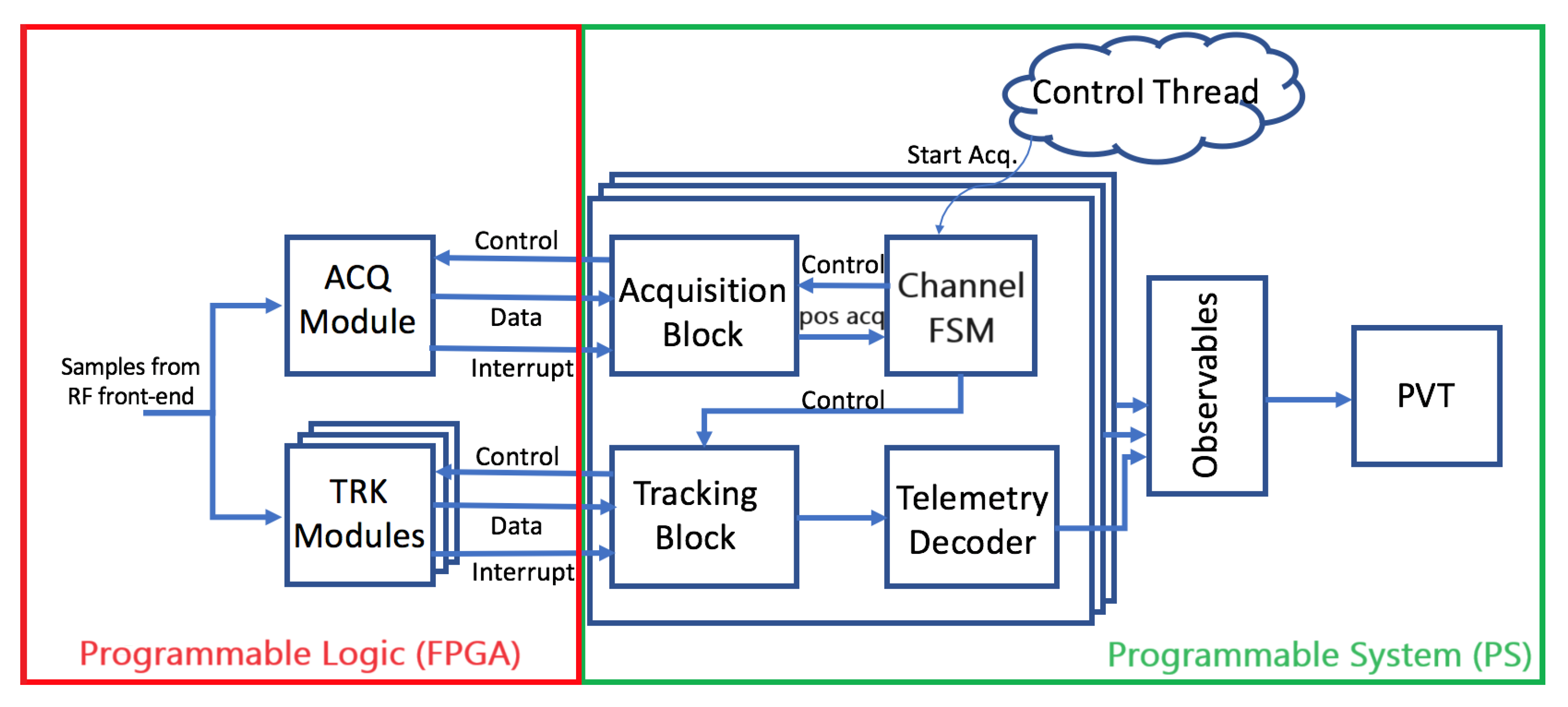
- 1.
- The software running in the processing system configures the multicorrelator hardware accelerators with updated parameters: coherent integration time, Doppler frequency correction, etc.
- 2.
- The multicorrelator hardware accelerator captures a new batch of samples and processes the samples on the fly.
- 3.
- The multicorrelator hardware accelerator finishes processing the received samples.
- 4.
- The multicorrelator hardware accelerator interrupts the processing system and waits for the multicorrelation results to be read. The software running in the processing system reads those results and operates the tracking loop.
3.2.1. Acquisition Hardware Accelerator
| Variable | Definition |
|---|---|
| Minimum tested Doppler frequency | |
| Maximum tested Doppler frequency | |
| Doppler frequency span | |
| Tested Doppler frequency | |
| Doppler search step | |
| Received GNSS signal input sample stream | |
| Sampling period | |
| Fast Fourier transform (FFT) of the pseudo-random noise (PRN) code | |
| Cross-ambiguity function (CAF) |
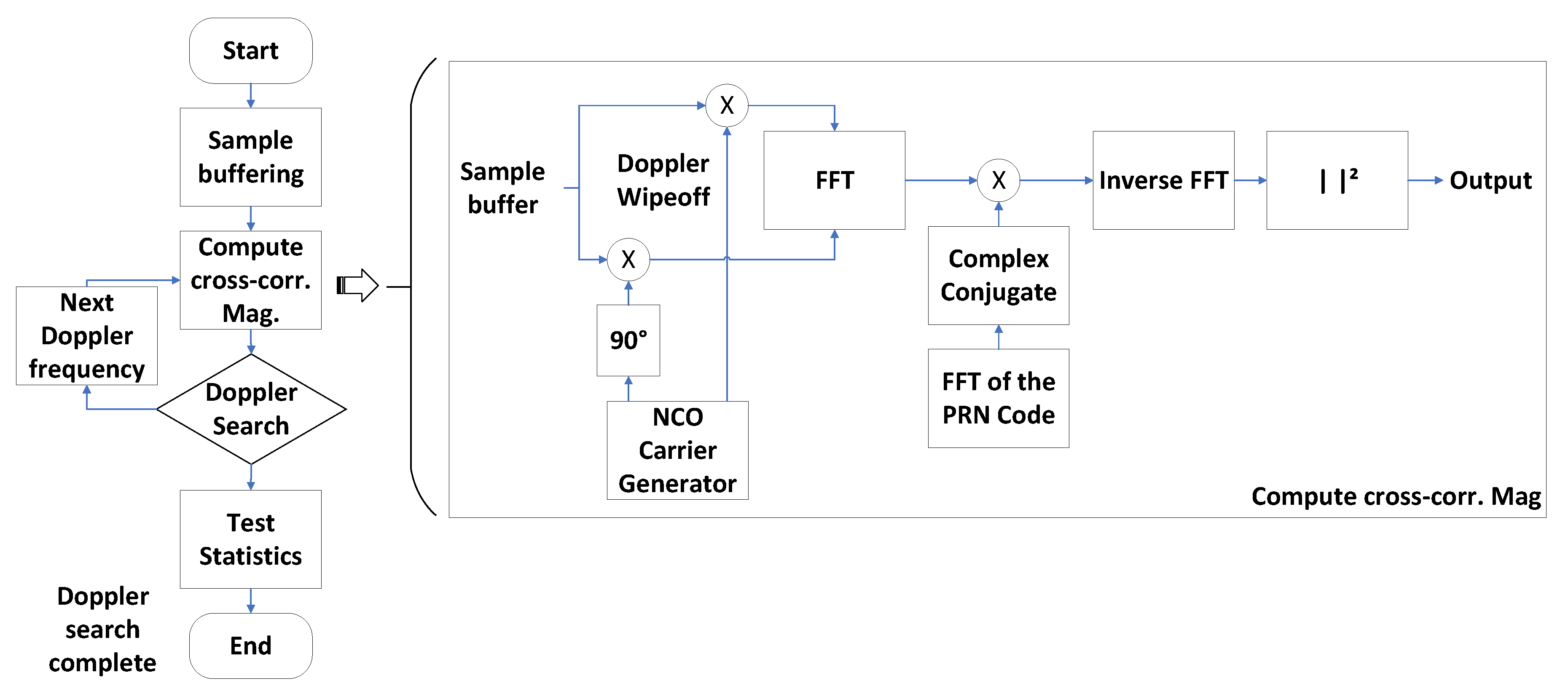
| Algorithm 1 Acquisition hardware accelerator |
|
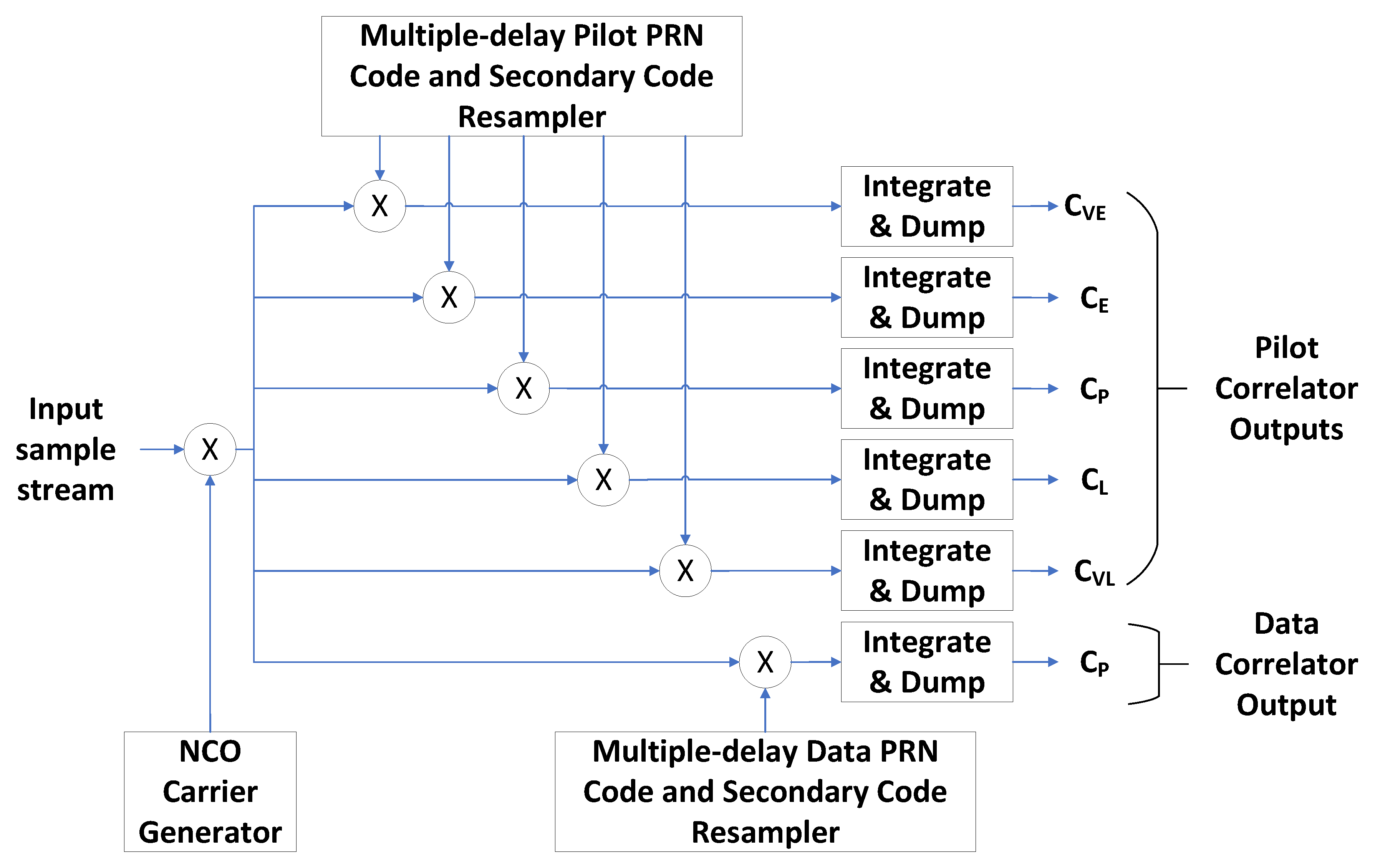
3.2.2. Tracking Multicorrelator Hardware Accelerators
| Variable | Definition |
|---|---|
| N | Number of samples indicating coherent integration time. |
| Estimated Doppler frequency | |
| Received GNSS signal input sample stream | |
| Sampling period | |
| PRN code | |
| Secondary code | |
| Correlation of the incoming signal with the PRN code | |
| Very Early correlator output | |
| Early correlator output | |
| Prompt correlator output | |
| Late correlator output | |
| Very Late correlator output |

| Algorithm 2 Tracking multicorrelator hardware accelerator |
|
| Signal | Configuration |
|---|---|
| GPS L1 C/A | E, P, L |
| Galileo E1b/c | VE, E, P, L, VL (Pilot Component) |
| P (Data Component) | |
| GPS L5 | E, P, L (Pilot Component) |
| P (Data Component) | |
| Galileo E5a | E, P, L (Pilot Component) |
| P (Data Component) |
3.3. Software Architecture

4. Design Methodology
- Hardware/software design flow: The system is divided into hardware and software sections that are designed independently, using dedicated tools for each. The designer searches for an optimal partitioning and assignment of tasks between the software running in the embedded processor and the hardware implemented in the FPGA, with the objectives of minimizing power consumption and taking advantage of the FPGA’s massively parallel architecture. Software and hardware development are followed by integration testing, where the FPGA and the software components are combined and tested to confirm that they interact according to their requirements [54].
- Software-oriented, hardware/software co-design flow: the functionality of the whole system is described at a high level of abstraction using software code or block-based design techniques. The tools can then quickly partition hardware and software elements in the SoC-FPGA in different ways according to the designer’s commands, and all the communication interfaces between the FPGA and the software are automatically managed by the tools [54].
| Design Step | Explanation |
|---|---|
| Step 1: Software Design | Implements and validates the GNSS algorithms in software, using GNSS-SDR |
| Step 2: FPGA Design | Implements the FPGA hardware accelerators. Modifies the GNSS-SDR source code to use the hardware accelerators when the option to use an FPGA is enabled. |
| Step 3: System Integration | Integrates the software and the FPGA components and tests the whole system in an SoC-FPGA platform |
4.1. Software Receiver Design Methodology
4.2. SoC-FPGA-Based Receiver Design Methodology
- The first step consists of the implementation of the FPGA design containing the sample conditioning module, the acquisition and tracking modules, and the PS/PL interface shown in Figure 2.
- The second step is the creation of an embedded GNU/Linux system for the SoC embedded processor and a GNU/Linux software development kit (SDK). The SDK is then used to cross-compile GNSS-SDR for the embedded platform.
4.2.1. FPGA Design Process
- The first step is the implementation of the acquisition and tracking multicorrelator hardware accelerators. The FPGA hardware accelerators are implemented as separate FPGA projects, and they are packaged in the form of FPGA IP cores. FPGA IPs are pre-designed, reusable blocks of hardware functionality or components that can be integrated into FPGA designs. These IP cores are typically provided by FPGA manufacturers, third-party vendors, or open-source communities to simplify the development of complex FPGA-based systems
- The second step is the creation of an FPGA project implementing the sample conditioning, the PS/PL interface blocks, and the sample buffers shown in Figure 3. The designer imports the required acquisition and tracking multicorrelator FPGA IP cores into the FPGA project and connects them to the PS/PL interface and to the sample buffers if necessary.
4.2.2. Configuring and Building the Embedded GNU/Linux System and Cross-Compiling GNSS-SDR for the Embedded Platform
- The first step is to create a Petalinux project for the target SoC-FPGA platform
- The second step is to import the compiled FPGA design into the Petalinux project.
- The third step is to configure the embedded GNU/Linux system. The designers shall add the software libraries that are essential for the execution of GNSS-SDR, and any other software libraries that may be considered. This step is usually performed using the Petalinux tools. The designers may also configure the device tree, describing the various hardware accelerators that are accessible from the GNU/Linux system. The device tree is a file containing information about the board and its hardware, including the FPGA hardware accelerators.
- The fourth step is to cross-compile the GNU/Linux system for the embedded processor. The cross-compiled system contains the boot files, the OS kernel and file system, the FPGA bitstream describing the FPGA logic, and a device tree blob, which is a compiled version of the device tree.
- The fifth step is to create a software development kit (SDK). This can be done using Petalinux commands.
- The last step is to use the SDK to cross-compile GNSS-SDR for the embedded processor, using the appropriate flags telling the system to offload the computationally expensive signal processing functions to the FPGA.
5. Proof of Concept Demonstrators
| Device | Board | SoC-FPGA Platform | RFFE | Size |
|---|---|---|---|---|
| Spaceborne GNSS receiver [15] | ADRV9361-Z7035 Evaluation Board [69] | Zynq 7000 XC7Z035-L2 FBG676I [56] | AD9361 RF Agile Transceiver [70] (integrated in the evaluation board) | 100 mm × 62 mm |
| GNSS Rebroadcaster [16] | ADRV9361-Z7035 Evaluation Board [69] | Zynq 7000 XC7Z035-L2 FBG676I [56] | AD9361 RF Agile Transceiver [70] (integrated in the evaluation board) | 100 mm × 62 mm |
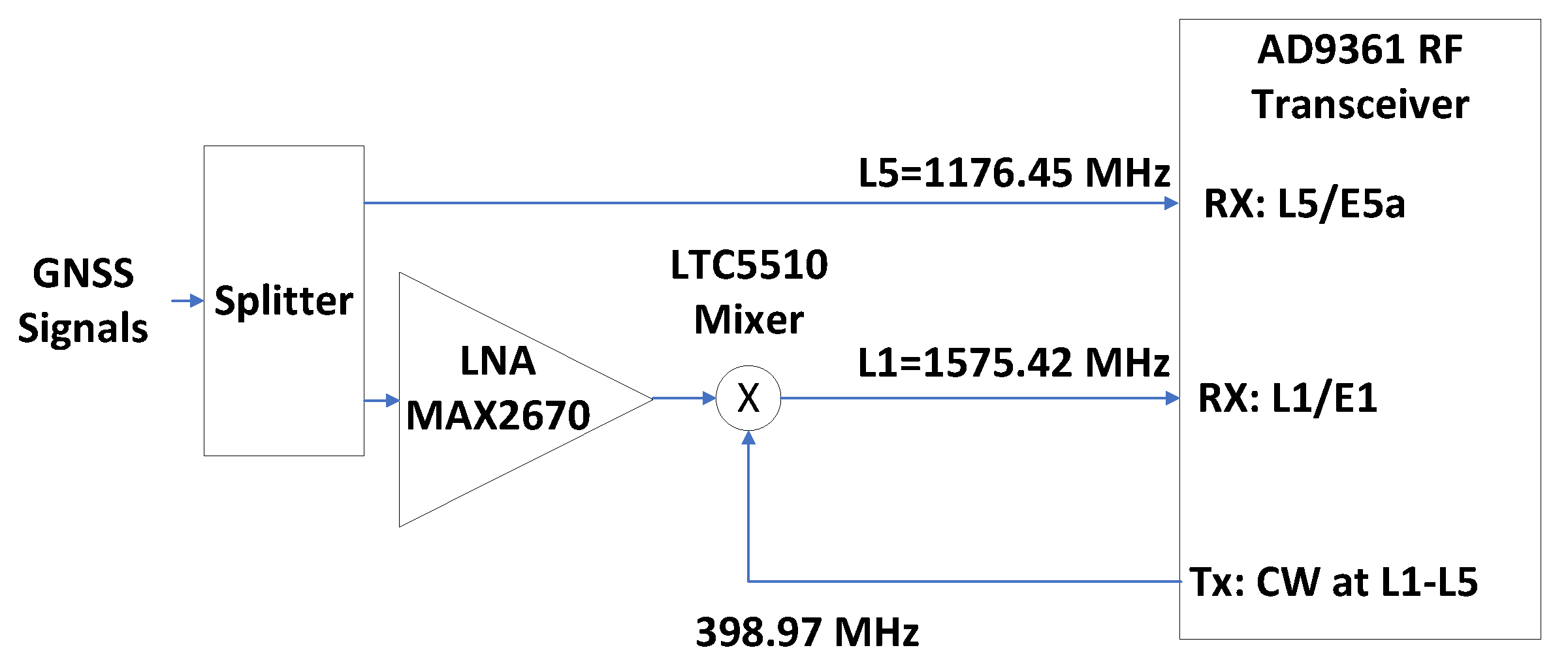
| General Purpose GNSS Receiver | Zynq UltraScale+ MPSoC ZCU102 Development Board [71] | Zynq ULtrascale+ XC7ZU9EG-2FFVB1156E [55] | AD-FMCOMMS5-EBZ [72] | 23.749 cm × 24.384 cm (ZCU102 Board), 14 cm × 9 cm (RFFE) |
5.1. Spaceborne GNSS Receiver
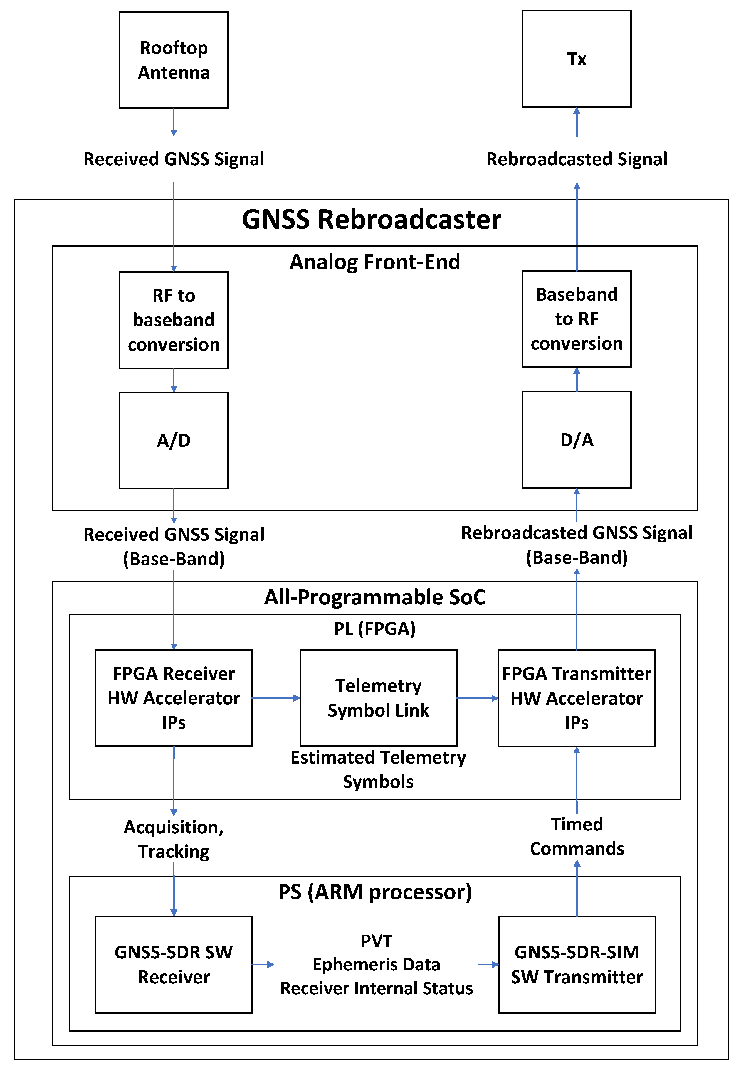
5.2. GNSS Rebroadcaster

5.3. General Purpose GNSS Receiver

6. Results
6.1. Receiver Sensitivity
6.1.1. Acquisition Sensitivity
| GNSS System | Acquisition Sensitivity (dB-Hz) |
|---|---|
| GPS L1 C/A | 37 |
| Galileo E1b/c | 39 |
| GPS L5 | 38 |
| Galileo E5a | 38 |
6.1.2. Tracking Sensitivity
| GNSS System | Acquisition Sensitivity (dB-Hz) |
|---|---|
| GPS L1 C/A | 26 |
| Galileo E1b/c | 28 |
| GPS L5 | 29 |
| Galileo E5a | 29 |
6.2. Multi-Frequency and Multi-Constellation Operating Modes
| GNSS Signals | Total Number of Signals |
|---|---|
| 12 GPS L1 C/A | 12 |
| 12 Galileo E1b/c | 12 |
| 12 GPS L5 | 12 |
| 12 Galileo E5a | 12 |
| 12 GPS L1 C/A + 12 Galileo E1b/c | 24 |
| 12 GPS L5 + 12 Galileo E5a | 24 |
| 12 GPS L1 C/A + 12 GPS L5 | 24 |
| 12 Galileo E1b/c + 12 Galileo E5a | 24 |
| 10 GPS L1 C/A + 10 Galileo E1b/c + 10 GPS L5 + 10 Galileo E5a | 40 |
6.3. Observables Quality
6.3.1. RMSE of the Carrier Phase

6.3.2. RMSE of the Code Phase

6.4. Precision of the Navigation Solutions
| Measure | Formula | Confidence Region Probability |
|---|---|---|
| 2D 2DRMS | 95% | |
| 2D DRMS | 65% | |
| 2D CEP | , if | 50% |
| Measure | Formula | Confidence Region Probability |
|---|---|---|
| 3D 99% SAS | 99% | |
| 3D 90% SAS | 90% | |
| 3D MRSE | 61% | |
| 3D SEP | 50% |
| Measure | Results (Test 1) [m] | Results (Test 2) [m] | Confidence Region Probability |
|---|---|---|---|
| 2D 2DRMS | 6.9 | 4.9 | 95% |
| 2D DRMS | 3.4 | 2.4 | 65% |
| 2D CEP | 2.8 | 2.0 | 50% |
| Measure | Results (Test 1) [m] | Results (Test 2) [m] | Confidence Region Probability |
|---|---|---|---|
| 3D 99% SAS | 9.6 | 8.6 | 99% |
| 3D 90% SAS | 7.1 | 6.4 | 90% |
| 3D MRSE | 5.1 | 4.9 | 61% |
| 3D SEP | 4.3 | 3.9 | 50% |
6.5. Accuracy of the Navigation Solutions Using an LEO Scenario
| Measure | Result |
|---|---|
| 3D Position RMSE | 1.2 m |
| 3D Position mean error | 1.1 m |
| 3D Position standard deviation | 0.5 m |
| 3D Velocity RMSE | 0.2 m/s |
| 3D Velocity mean error | 0.2 m/s |
| 3D Velocity standard deviation | 0.1 m/s |
6.6. Power Consumption
7. Conclusions
Author Contributions
Funding
Institutional Review Board Statement
Informed Consent Statement
Data Availability Statement
Conflicts of Interest
Sample Availability
Abbreviations
| GNSS | Global Navigation Satellite System |
| IC | Integrated Circuit |
| SoC-FPGA | System-on-Chip Field-Programmable Gate Array |
| SDR | Software-Defined Radio |
| LEO | Low Earth Orbit |
| ASIC | Application Specific Integrated Circuit |
| FOSS | Free and Open Source Software |
| CPU | Central Processing Unit |
| COTS | Commercial Off The Shelf |
| RFFE | Radio-Frequency Front-End |
| PC | Personal Computer |
| IP | Intellectual Property |
| GPS | Global Positioning System |
| GPU | Graphics Processing Unit |
| DSP | Digital Signal Processor |
| RF | Radio Frequency |
| PS | Processing System |
| PL | Programmable Logic |
| DDR | Double Data Rate |
| RINEX | Receiver Independent Exchange Format Version |
| RTCM | Radio Technical Commission for Maritime Services |
| NMEA | National Marine Electronics Association |
| DMA | Direct Memory Access |
| AMBA | Advanced Microcontroller Bus Architecture |
| AXI4 | Advanced eXtensible Interface |
| OS | Operating System |
| SD | Secure Digital |
| AMD | Advanced Micro Devices |
| MPSoC | Multi-Processor System on Chip |
| A/D | Analog-to-Digital Converter |
| PCPS | Parallel Code Phase Search |
| PRN | Pseudo-Random Noise |
| CAF | Cross-Ambiguity Function |
| FFT | Fast Fourier Transform |
| PVT | Position, Velocity, and Time |
| FSM | Finite State Machine |
| GPL | General Public License |
| PLL | Phase-Locked Loop |
| DLL | Delay-Locked Loop |
| LNA | Low-Noise Amplifier |
| AGC | Automatic Gain Control |
| SDK | Software Development Kit |
| HLS | High-Level Synthesis |
| VHDL | Very-High-Speed Integrated Circuit Hardware Description Language |
| RTL | Register Transfer Logic |
| CW | Continuous Wave |
| SFF | Small Form Factor |
| RMSE | Root Mean Square Error |
| Msps | Mega samples per second |
| ECEF | Earth-Centered, Earth-Fixed |
| DRMS | Distance Root Mean Square |
| CEP | Circular Error Probability |
| SAS | Spherical Accuracy Standard |
| MRSE | Mean Radial Spherical Error |
| SEP | Spherical Error Probable |
Appendix A
| Acquisition GPS L1 C/A | Doppler Max | 5000 Hz |
| Doppler Step | 500 Hz | |
| Threshold | 2.5 | |
| Downsampling Factor | 4 | |
| Acquisition GPS L5 | Doppler Max | 500 Hz |
| Doppler Step | 250 Hz | |
| Threshold | 2.5 | |
| Assistance to acquisition from primary to secondary band | Enabled | |
| Acquisition Galileo E1b/c | Doppler Max | 5000 Hz |
| Doppler Step | 250 Hz | |
| Threshold | 2.5 | |
| Downsampling Factor | 4 | |
| Acquisition Galileo E5a | Doppler Max | 500 Hz |
| Doppler Step | 125 Hz | |
| Threshold | 2.5 | |
| Assistance to acquisition from primary to secondary band | Enabled |
| Tracking GPS L1 C/A | Coherent integration time | 20 ms |
| Early–Late space chips | 0.5 | |
| Early–Late space narrow chips | 0.1 | |
| PLL filter bandwidth | 35 Hz | |
| PLL filter bandwidth (narrow correlator configuration) | 7.5 Hz | |
| DLL filter bandwidth | 2 Hz | |
| DLL filter bandwidth (narrow correlator configuration) | 0.5 Hz | |
| Tracking GPS L5 | Coherent integration time | 20 ms |
| Early–Late space chips | 0.5 | |
| Early–Late space narrow chips | 0.1 | |
| PLL filter bandwidth | 20 Hz | |
| PLL filter bandwidth (narrow correlator configuration) | 7.5 Hz | |
| DLL filter bandwidth | 1.5 Hz | |
| DLL filter bandwidth (narrow correlator configuration) | 0.5 Hz | |
| Tracking Galileo E1b/c | Coherent integration time | 20 ms |
| Early–Late space chips | 0.25 | |
| Very Early–Late space chips | 0.5 | |
| Early–Late space narrow chips | 0.15 | |
| Very Early–Late space narrow chips | 0.5 | |
| PLL filter bandwidth | 15 Hz | |
| PLL filter bandwidth (narrow correlator configuration) | 7.5 Hz | |
| DLL filter bandwidth | 0.75 Hz | |
| DLL filter bandwidth (narrow correlator configuration) | 0.5 Hz | |
| Tracking Galileo E5a | Coherent integration time | 20 ms |
| Early–Late space chips | 0.5 | |
| Early–Late space narrow chips | 0.1 | |
| PLL filter bandwidth | 20 Hz | |
| PLL filter bandwidth (narrow correlator configuration) | 7.5 Hz | |
| DLL filter bandwidth | 1.5 Hz | |
| DLL filter bandwidth (narrow correlator configuration) | 0.5 Hz |
| General | Positioning Mode | Single |
| Receiver Autonomous Integrity Monitoring (RAIM) Fault Detection and Exclusion (FDE) | Enabled | |
| Iono Model | Broadcast | |
| Trop Model | Saastamoinen | |
| PVT Output Rate | 1 s | |
| Use unhealthy sats | Disabled | |
| PVT Kalman Filter | Standard deviation of the position estimations | 1 m |
| Standard deviation of the velocity estimations | 0.1 m/s | |
| Standard deviation of the dynamic system model for position | 0.01 m | |
| Standard deviation of the dynamic system model for velocity | 0.001 m/s |
Appendix B
| Acquisition GPS L1 C/A | Doppler Max | 50,000 Hz |
| Doppler Step | 250 Hz | |
| Threshold | 2.5 | |
| Downsampling Factor | 4 | |
| Acquisition GPS L5 | Doppler Max | 5000 Hz |
| Doppler Step | 250 Hz | |
| Threshold | 2.5 | |
| Assistance to acquisition from primary to secondary band | Enabled | |
| Acquisition Galileo E1b/c | Doppler Max | 50,000 Hz |
| Doppler Step | 250 Hz | |
| Threshold | 2.5 | |
| Downsampling Factor | 4 | |
| Acquisition Galileo E5a | Doppler Max | 5000 Hz |
| Doppler Step | 250 Hz | |
| Threshold | 2.5 | |
| Assistance to acquisition from primary to secondary band | Enabled |
| Tracking GPS L1 C/A | Coherent integration time | 20 ms |
| Early–Late space chips | 0.25 | |
| Early–Late space narrow chips | 0.15 | |
| PLL filter bandwidth | 35 Hz | |
| PLL filter bandwidth (narrow correlator configuration) | 5.0 Hz | |
| DLL filter bandwidth | 2 Hz | |
| DLL filter bandwidth (narrow correlator configuration) | 0.5 Hz | |
| Enable FLL pull-in | true | |
| FLL filter bandwidth | 10 Hz | |
| High dynamics | true | |
| Tracking GPS L5 | Coherent integration time | 5 ms |
| Early–Late space chips | 0.5 | |
| Early–Late space narrow chips | 0.5 | |
| PLL filter bandwidth | 50 Hz | |
| PLL filter bandwidth (narrow correlator configuration) | 30 Hz | |
| DLL filter bandwidth | 4 Hz | |
| DLL filter bandwidth (narrow correlator configuration) | 2 Hz | |
| Enable FLL pull-in | true | |
| FLL filter bandwidth | 2.5 Hz | |
| High dynamics | true | |
| Early–Late space chips | 0.15 | |
| Very Early–Late space chips | 0.5 | |
| Early–Late space narrow chips | 0.15 | |
| Very Early–Late space narrow chips | 0.5 | |
| PLL filter bandwidth | 15 Hz | |
| PLL filter bandwidth (narrow correlator configuration) | 5.0 Hz | |
| DLL filter bandwidth | 0.75 Hz | |
| DLL filter bandwidth (narrow correlator configuration) | 0.5 Hz | |
| Enable FLL pull-in | true | |
| FLL filter bandwidth | 10 Hz | |
| High dynamics | true | |
| Tracking Galileo E5a | Coherent integration time | 5 ms |
| Early–Late space chips | 0.5 | |
| Early–Late space narrow chips | 0.5 | |
| PLL filter bandwidth | 50 Hz | |
| PLL filter bandwidth (narrow correlator configuration) | 30 Hz | |
| DLL filter bandwidth | 4.0 Hz | |
| DLL filter bandwidth (narrow correlator configuration) | 2.0 Hz | |
| Enable FLL pull-in | true | |
| FLL filter bandwidth | 2.5 Hz | |
| High dynamics | true |
| General | Positioning Mode | Single |
| Receiver Autonomous Integrity Monitoring (RAIM) Fault Detection and Exclusion (FDE) | Enabled | |
| Iono Model | OFF | |
| Trop Model | OFF | |
| PVT Output Rate | 20 ms | |
| Use unhealthy sats | Disabled | |
| PVT Kalman Filter | Standard deviation of the position estimations | 1 m |
| Standard deviation of the velocity estimations | 0.1 m/s | |
| Standard deviation of the dynamic system model for position | 0.01 m | |
| Standard deviation of the dynamic system model for velocity | 0.001 m/s |
References
- Janssen, T.; Koppert, A.; Berkvens, R.; Weyn, M. A Survey on IoT Positioning Leveraging LPWAN, GNSS, and LEO-PNT. IEEE Internet Things J. 2023, 10, 11135–11159. [Google Scholar] [CrossRef]
- Ogaja, C.A. Augmented Reality: A GNSS Use Case. In Introduction to GNSS Geodesy: Foundations of Precise Positioning Using Global Navigation Satellite Systems; Springer International Publishing: Cham, Switzerland, 2022; pp. 3–12. [Google Scholar] [CrossRef]
- Shimazu, K.; Makabe, K.; Nishii, N.; Mori, R.; Harada, N.; Sashida, H.; Oikawa, K. Emergency Warning Services via GNSS Signals. In Proceedings of the 2020 IEEE Aerospace Conference, Big Sky, MT, USA, 7–14 March 2020; pp. 1–16. [Google Scholar] [CrossRef]
- Xia, X.; Meng, Z.; Han, X.; Li, H.; Tsukiji, T.; Xu, R.; Zheng, Z.; Ma, J. An automated driving systems data acquisition and analytics platform. Transp. Res. Part C Emerg. Technol. 2023, 151, 104120. [Google Scholar] [CrossRef]
- Xia, X.; Bhatt, N.P.; Khajepour, A.; Hashemi, E. Integrated Inertial-LiDAR-Based Map Matching Localization for Varying Environments. IEEE Trans. Intell. Veh. 2023, 8, 4307–4318. [Google Scholar] [CrossRef]
- Meng, Z.; Xia, X.; Xu, R.; Liu, W.; Ma, J. HYDRO-3D: Hybrid Object Detection and Tracking for Cooperative Perception Using 3D LiDAR. IEEE Trans. Intell. Veh. 2023, 8, 4069–4080. [Google Scholar] [CrossRef]
- Arribas, J.; Fernández-Prades, C.; Closas, P. GESTALT: A Testbed For Experimentation And Validation of GNSS Software Receivers. In Proceedings of the 28th International Technical Meeting of the Satellite Division of The Institute of Navigation (ION GNSS+ 2015), Tampa, FL, USA, 14–18 September 2015; pp. 3222–3234. [Google Scholar]
- Egea-Roca, D.; Arizabaleta-Diez, M.; Pany, T.; Antreich, F.; López-Salcedo, J.A.; Paonni, M.; Seco-Granados, G. GNSS User Technology: State-of-the-Art and Future Trends. IEEE Access 2022, 10, 39939–39968. [Google Scholar] [CrossRef]
- Fernández-Prades, C.; Arribas, J.; Majoral, M.; Vilà-Valls, J.; García-Rigo, A.; Hernández-Pajares, M. An Open Path from the Antenna to Scientific-grade GNSS Products. In Proceedings of the 6th ESA Intl. Colloquium on Scientific and Fundamental Aspects of GNSS/Galileo, Valencia, Spain, 25–27 October 2017. [Google Scholar]
- Khan, M.; Rehman, F. Free and Open Source Software: Evolution, Benefits and Characteristics. Int. J. Emerg. Trends Technol. Comput. Sci. (IJETTCS) 2012, 1, 1–7. [Google Scholar]
- Fernández-Prades, C.; Arribas, J.; Closas, P.; Aviles, C.; Luis, E. GNSS-SDR: An Open Source Tool for Researchers and Developers. In Proceedings of the 24th International Technical Meeting of the Satellite Division of The Institute of Navigation (ION GNSS 2011), Portlan, OR, USA, 20–23 September 2011; pp. 780–794. [Google Scholar]
- GNSS-SDR. An Open-Source Global Navigation Satellite Systems Software-Defined Receiver. Available online: https://gnss-sdr.org/ (accessed on 23 November 2023).
- Grenier, A.; Lohan, E.S.; Ometov, A.; Nurmi, J. A Survey on Low-Power GNSS. IEEE Commun. Surv. Tutor. 2023, 25, 1482–1509. [Google Scholar] [CrossRef]
- Majoral, M.; Fernández-Prades, C.; Arribas, J. Implementation of GNSS Receiver Hardware Accelerators in All-programmable System-On-Chip Platforms. In Proceedings of the 31st International Technical Meeting of the Satellite Division of The Institute of Navigation (ION GNSS+ 2018), Miami, FL, USA, 24–28 September 2018; pp. 4215–4230. [Google Scholar]
- Fernández-Prades, C.; Arribas, J.; Majoral, M.; Ramos, A.; Vilá-Valls, J.; Giordano, P. A Software-Defined Spaceborne GNSS Receiver. In Proceedings of the 2018 9th ESA Workshop on Satellite NavigationTechnologies and European Workshop on GNSS Signals and Signal Processing (NAVITEC), Noordwijk, The Netherlands, 5–7 December 2018; pp. 1–9. [Google Scholar] [CrossRef]
- Majoral, M.; Arribas, J.; Fernández-Prades, C. Implementation of a GNSS Rebroadcaster in an All-Programmable System-On-Chip Platform. In Proceedings of the 2022 10th Workshop on Satellite Navigation Technology (NAVITEC), Noordwijk, The Netherlands, 5–7 April 2022; pp. 1–9. [Google Scholar] [CrossRef]
- Doberstein, D. Fundamentals of GPS Receivers: A Hardware Approach, 1st ed.; Springer: New York, NY, USA, 2012. [Google Scholar] [CrossRef]
- Tsui, J. Fundamentals of Global Positioning System Receivers: A Software Approach, 2nd ed.; John Wiley & Sons, Inc.: Hoboken, NJ, USA, 2005. [Google Scholar] [CrossRef]
- Borre, K.; Akos, D.; Bertelsen, N.; Rinder, P.; Jensen, S. A Software-Defined GPS and Galileo Receiver: A Single-Frequency Approach, 1st ed.; Birkhäuser: Boston, MA, USA, 2007. [Google Scholar] [CrossRef]
- Yu, L. BDS/GPS Dual-Mode Software Receiver: Principles and Implementation Technology, 1st ed.; Springer: Singapore, 2021. [Google Scholar] [CrossRef]
- Borre, K.; Fernández-Hernández, I.; López-Salcedo, J.A.; Bhuiyan, M.Z.H. GNSS Software Receivers, 1st ed.; Cambridge University Press: Cambridge, UK, 2022. [Google Scholar] [CrossRef]
- Krumvieda, K.; Madhani, P.; Cloman, C.; Olson, E.; Thomas, J.; Axelrad, P.; Kober, W. A Complete IF Software GPS Receiver: A Tutorial about the Details. In Proceedings of the 14th International Technical Meeting of the Satellite Division of The Institute of Navigation (ION GPS 2001), Salt Lake City, UT, USA, 11–14 September 2001; pp. 789–829. [Google Scholar]
- Chakravarthy, V.; Tsui, J.; Lin, D.; Schamus, J. Software GPS Receiver. GPS Solut. 2001, 5, 63–70. [Google Scholar] [CrossRef]
- Principe, F.; Bacci, G.; Giannetti, F.; Luise, M. Software-Defined Radio Technologies for GNSS Receivers: A Tutorial Approach to a Simple Design and Implementation. Int. J. Navig. Obs. 2011, 2011, 979815. [Google Scholar] [CrossRef]
- Akos, D.M. A Software Radio Approach to Global Navigation Satellites System Receiver Design. Ph.D. Thesis, Ohio University, Athens, OH, USA, 1997. Available online: https://etd.ohiolink.edu/acprod/odb_etd/etd/r/1501/10?clear=10&p10_accession_num=ohiou1174615606 (accessed on 23 November 2023).
- Ledvina, B.M.; Powell, S.P.; Kintner, P.M.; Psiaki, M.L. A 12–Channel Real–Time GPS L1 Software Receiver. In Proceedings of the 2003 National Technical Meeting of The Institute of Navigation, Anaheim, CA, USA, 22–24 January 2003; pp. 767–782. [Google Scholar]
- Fantino, M.; Molino, A.; Nicola, M. N-Gene GNSS Receiver: Benefits of Software Radio in Navigation. In Proceedings of the European Navigation Conference (ENC 2009), Napoli, Italy, 3–6 May 2009. [Google Scholar]
- Stöber, C.; Anghileri, M.; Sicramaz Ayaz, A.; Dötterböck, D.; Krämer, I.; Kropp, V.; Won, J.H.; Eissfeller, B.; Güixens, D.S.; Pany, T. ipexSR: A real-time multi-frequency software GNSS receiver. In Proceedings of the ELMAR-2010, Zadar, Croatia, 15–17 September 2010; pp. 407–416. [Google Scholar]
- Gamba, M.T.; Nicola, M.; Falletti, E. Performance assessment of an ARM-based dual-constellation GNSS software receiver. In Proceedings of the 2015 International Conference on Localization and GNSS (ICL-GNSS), Gothenburg, Sweden, 22–24 June 2015; pp. 1–6. [Google Scholar] [CrossRef]
- Pei, Y.; Chen, H.; Pei, B. Implementation of GPS Software Receiver Based on GNU Radio. In Proceedings of the 2018 Cross Strait Quad-Regional Radio Science and Wireless Technology Conference (CSQRWC), Xuzhou, China, 21–24 July 2018; pp. 1–3. [Google Scholar] [CrossRef]
- Petovello, M.; O’Driscoll, C.; Lachapelle, G.; Borio, D.; Murtaza, H. Architecture and Benefits of an Advanced GNSS Software Receiver. J. Glob. Position. Syst. 2008, 7, 156–168. [Google Scholar] [CrossRef]
- Hobiger, T.; Gotoh, T.; Amagai, J.; Koyama, Y.; Kondo, T. A GPU based real-time GPS software receiver. GPS Solut. 2010, 14, 207–216. [Google Scholar] [CrossRef]
- Tolman, B.W.; Harris, R.B.; Gaussiran, T.; Munton, D.; Jon, L.; Mach, R.; Nelsen, S.; Renfro, B.; Schlossberg, D. The GPS Toolkit… Open Source GPS Software. In Proceedings of the 17th International Technical Meeting of the Satellite Division of The Institute of Navigation (ION GNSS 2004), Long Beach, CA, USA, 21–24 September 2004; pp. 2044–2053. [Google Scholar]
- Kovar, P.; Vejrazka, F. Software radio and its applications in GNSS. In Proceedings of the Elmar-2004—46th International Symposium on Electronics in Marine, Zadar, Croatia, 16–18 June 2004; pp. 16–21. [Google Scholar]
- Soghoyan, A.; Suleiman, A.; Akopian, D. A Development and Testing Instrumentation for GPS Software Defined Radio with Fast FPGA Prototyping Support. IEEE Trans. Instrum. Meas. 2014, 63, 2001–2012. [Google Scholar] [CrossRef]
- Garzia, F.; Rügamer, A.; Koch, R.; Neumaier, P.; Serezhkina, E.; Overbeck, M.; Rohmer, G. Experimental multi-FPGA GNSS receiver platform. In Proceedings of the 2014 24th International Conference on Field Programmable Logic and Applications (FPL), Munich, Germany, 2–4 September 2014; pp. 1–4. [Google Scholar] [CrossRef]
- Larosa, F.S. Design, Simulation, Implementation and Testing of Search and Tracking Modules for a FPGA-Based GPS Receiver. In Proceedings of the 2019 X Southern Conference on Programmable Logic (SPL), Buenos Aires, Argentina, 10–12 April 2019; pp. 33–38. [Google Scholar] [CrossRef]
- Keshihaa Rudra Gana Dev, V.; Ranjani, G. An Optimized FPGA Architecture for GPS Signal Acquisition. In Proceedings of the 2022 IEEE 3rd Global Conference for Advancement in Technology (GCAT), Bangalore, India, 7–9 October 2022; pp. 1–6. [Google Scholar] [CrossRef]
- Spelat, M.; Dovis, F.; Girau, G.; Mulassano, P. A Flexible FPGA/DSP Board for GNSS Receivers Design. In Proceedings of the 2006 Ph.D. Research in Microelectronics and Electronics, Otranto, Italy, 12–15 June 2006; pp. 77–80. [Google Scholar] [CrossRef]
- Grondin, M.; Belasic, M.; Ries, L.; Issler, J.L.; Bataille, P.; Jobey, L.; Richard, G. A new operational low cost GNSS software receiver for microsatellites. In Proceedings of the 2010 5th ESA Workshop on Satellite Navigation Technologies and European Workshop on GNSS Signals and Signal Processing (NAVITEC), Noordwijk, The Netherlands, 8–10 December 2010; pp. 1–5. [Google Scholar] [CrossRef]
- Avanzi, A.; Tortora, P.; Garcia-Rodriguez, A. Design and Implementation of a Novel Multi-constellation FPGA-based Dual Frequency GNSS Receiver for Space Applications. In Proceedings of the 24th International Technical Meeting of the Satellite Division of The Institute of Navigation (ION GNSS 2011), Portland, OR, USA, 20–23 September 2011; pp. 746–752. [Google Scholar]
- Fantinato, S.; Foglia, L.; Iacone, P.; Rovelli, D.; Facchinetti, C.; Tuozzi, A. PEGASUS -GNSS receiver platform for safety of life user segment. In Proceedings of the 2012 6th ESA Workshop on Satellite Navigation Technologies (Navitec 2012) & European Workshop on GNSS Signals and Signal Processing, Noordwijk, The Netherlands, 5–7 December 2012; pp. 1–8. [Google Scholar] [CrossRef]
- Kappen, G.; Haettich, C.; Meurer, M. Towards a robust multi-antenna mass market GNSS receiver. In Proceedings of the 2012 IEEE/ION Position, Location and Navigation Symposium, Myrtle Beach, SC, USA, 23–26 April 2012; pp. 291–300. [Google Scholar] [CrossRef]
- Wang, B.S.; Iv, S.W.; Yang, D.K.; Zhang, Q.S. A New Solution to GNSS Receiver Baseband Signal Processing SOC Platform Based on OpenRISC Processor. In Proceedings of the 2011 7th International Conference on Wireless Communications, Networking and Mobile Computing, Wuhan, China, 23–25 September 2011; pp. 1–4. [Google Scholar] [CrossRef]
- Raasakka, J.; Hurskainen, H.; Nurmi, J. GNSS baseband processing in a multi-core platform. In Proceedings of the 2011 International Conference on Localization and GNSS (ICL-GNSS), Tampere, Finland, 29–30 June 2011; pp. 42–46. [Google Scholar] [CrossRef]
- Fridman, A.; Semenov, S. System-on-Chip FPGA-based GNSS receiver. In Proceedings of the East-West Design & Test Symposium (EWDTS 2013), Rostov on Don, Russia, 27–30 September 2013; pp. 1–7. [Google Scholar] [CrossRef]
- Buttgereit, J.; Schwarte, T.; Kappen, G.C. Design and Implementation of a Software Defined Radio GNSS Receiver Based on OpenCL. In Proceedings of the 2020 IEEE/ION Position, Location and Navigation Symposium (PLANS), Portland, OR, USA, 20–23 April 2020; pp. 1237–1246. [Google Scholar] [CrossRef]
- Priot, B.; Dion, A.; Beaugendre, G.; Kasaraneni, R. Accurate Events Synchronization in a System-on-Chip Navigation Receiver. In Proceedings of the International Conference on Localization and GNSS, Nuremberg, Germany, 4–6 June 2019; pp. 1–5. [Google Scholar]
- Huang, K.Y.; Juang, J.C.; Tsai, Y.F.; Lin, C.T. Efficient FPGA Implementation of a Dual-Frequency GNSS Receiver with Robust Inter-Frequency Aiding. Sensors 2021, 21, 4634. [Google Scholar] [CrossRef] [PubMed]
- Guruprasad, S. FPGA-Based GNSS Receiver Design for Reflectometry Applications. Ph.D. Thesis, York University, Toronto, ON, Cadada, 2022. [Google Scholar]
- Kusswurm, D. X86-64 Core Architecture. In Modern X86 Assembly Language Programming; Apress: Berkeley, CA, USA, 2014; pp. 491–502. [Google Scholar] [CrossRef]
- Wang, K.C. ARM Architecture and Programming. In Embedded and Real-Time Operating Systems; Springer International Publishing: Cham, Switzerland, 2023; pp. 7–45. [Google Scholar]
- Crockett, L.H.; Elliot, R.A.; Enderwitz, M.A.; Stewart, R.W. The Zynq Book: Embedded Processing with the Arm Cortex-A9 on the Xilinx Zynq-7000 All Programmable Soc; Strathclyde Academic Media: Glasgow, UK, 2014. [Google Scholar]
- Crockett, L.H.; Northcote, D.; Ramsay, C.; Robinson, F.D.; Stewart, R.W. Exploring Zynq MPSoC: With PYNQ and Machine Learning Applications; Strathclyde Academic Media: Glasgow, UK, 2019. [Google Scholar]
- Advanced Micro Devices Inc. Zynq Ultrascale+ Device Technical Reference Manual. UG1085 (v2.3.1). 2023. Available online: https://docs.xilinx.com/r/en-US/ug1085-zynq-ultrascale-trm/Introduction-to-the-UltraScale-Architecture (accessed on 23 November 2023).
- Advanced Micro Devices Inc. Zynq-7000 All Programmable SoC Technical Reference Manual. UG585 (v1.14). 2023. Available online: https://docs.xilinx.com/r/en-US/ug585-zynq-7000-SoC-TRM (accessed on 23 November 2023).
- Advanced Micro Devices Inc. Zynq-7000 SoC Product Selection Guide. XMP097 (v1.3.2). 2019. Available online: https://docs.xilinx.com/v/u/en-US/zynq-7000-product-selection-guide (accessed on 23 November 2023).
- Advanced Micro Devices Inc. Zynq Ultrascale+ MPSoC Product Tables and Product Selection Guide. XMP104 (v2.6). 2022. Available online: https://docs.xilinx.com/v/u/en-US/zynq-ultrascale-plus-product-selection-guide (accessed on 23 November 2023).
- Arribas, J. GNSS Array-Based Acquisition: Theory and Implementation. Ph.D. Thesis, Universitat Politecnica de Catalunya (UPC), Barcelona, Spain, 2012. [Google Scholar]
- Kaplan, E.; Hegarty, C. Understanding GPS/GNSS: Principles and Applications, 3rd ed.; Artech House, Inc.: Norwood, MA, USA, 2017. [Google Scholar]
- Fernández-Prades, C.; Arribas, J.; Esteve, L.; Pubill, D.; Closas, P. An open source Galileo E1 software receiver. In Proceedings of the 2012 6th ESA Workshop on Satellite Navigation Technologies (Navitec 2012) & European Workshop on GNSS Signals and Signal Processing, Noordwijk, The Netherlands, 5–7 December 2012; pp. 1–8. [Google Scholar] [CrossRef]
- GNU Radio. A Free & Open-Source Software Development Toolkit. Available online: http://gnuradio.org (accessed on 23 November 2023).
- Advanced Micro Devices Inc. Vivado Design Suite User Guide: Release Notes, Installation, and Licensing. UG973 (v2022.2). 2022. Available online: https://www.xilinx.com/support/documents/sw_manuals/xilinx2022_1/ug973-vivado-release-notes-install-license.pdf (accessed on 23 November 2023).
- Advanced Micro Devices Inc. AMD University Program. Available online: https://www.amd.com/en/corporate/university-program.html (accessed on 23 November 2023).
- Advanced Micro Devices Inc. Vitis High-Level Synthesis User Guide. UG1399 (v2023.1). 2023. Available online: https://docs.xilinx.com/r/2023.1-English/ug1399-vitis-hls (accessed on 23 November 2023).
- Analog Devices Inc. HDL Reference Designs. Available online: https://wiki.analog.com/resources/fpga/docs/arch (accessed on 23 November 2023).
- Advanced Micro Devices Inc. PetaLinux Tools Documentation Reference Guide. UG1144 (v2023.2). 2023. Available online: https://docs.xilinx.com/r/2023.1-English/ug1144-petalinux-tools-reference-guide/Overview (accessed on 23 November 2023).
- Salvador, O.; Angolini, D. Embedded Linux Development Using Yocto Projects—Second Edition: Learn to Leverage the Power of Yocto Project to Build Efficient Linux-Based Products, 2nd ed.; Packt Publishing: Birmingham, UK, 2017. [Google Scholar]
- Analog Devices Inc. ADRV936x System on Module (SOM) SDR User Guide. Available online: https://wiki.analog.com/resources/eval/user-guides/adrv936x_rfsom (accessed on 23 November 2023).
- Analog Devices Inc. AD9361 Reference Manual. UG-570. Rev. A. 2015. Available online: https://www.analog.com/media/en/technical-documentation/user-guides/ad9361.pdf (accessed on 23 November 2023).
- Advanced Micro Devices Inc. ZCU102 Evaluation Board User Guide. UG1182 (v1.7). 2023. Available online: https://www.xilinx.com/support/documents/boards_and_kits/zcu102/ug1182-zcu102-eval-bd.pdf (accessed on 23 November 2023).
- Analog Devices Inc. AD-FMCOMMS5-EBZ User Guide. Available online: https://wiki.analog.com/resources/eval/user-guides/ad-fmcomms5-ebz (accessed on 23 November 2023).
- Abracon LLC. Abracon AST3TQ-T-40.000MHZ-50-C Datasheet. Rev. 04.02.15. 2015. Available online: https://abracon.com/Oscillators/AST3TQ.pdf (accessed on 23 November 2023).
- Tallysman Wireless Inc. TW8825 Datasheet. Rev. 1.2. 2019. Available online: https://www.tallysman.com/app/uploads/2019/10/TW8825_Datasheet_rev1_2.pdf (accessed on 23 November 2023).
- Arribas, J. GNSS-SIMULATOR. A Modular Multichannel GNSS Simulator Written in C++. Available online: https://bitbucket.org/jarribas/gnss-simulator/src/master/ (accessed on 23 November 2023).
- Van Dierendonck, A.; Fenton, P.; Ford, T. Theory and Performance of Narrow Correlator Spacing in a GPS Receiver. NAVIGATION J. Inst. Navig. 1992, 39, 265–284. [Google Scholar] [CrossRef]
- NovAtel Inc. GPS Position Accuracy Measures. APN-029. 2003. Available online: https://www.gnss.ca/novatel_app_notes/APN-029_GPS_Position_Accuracy_Measures_Application_Note (accessed on 23 November 2023).
- Fernández-Prades, C.; Arribas, J.; Closas, P. Turning a Television Into a GNSS Receiver. In Proceedings of the 26th International Technical Meeting of the Satellite Division of The Institute of Navigation (ION GNSS+ 2013), Nashville, TN, USA, 16–20 September 2013; pp. 1492–1507. [Google Scholar]
- Saastamoinen, J. Contributions to the theory of atmospheric refraction. Bull. Géod. (1946–1975) 1972, 105, 279–298. [Google Scholar] [CrossRef]
Disclaimer/Publisher’s Note: The statements, opinions and data contained in all publications are solely those of the individual author(s) and contributor(s) and not of MDPI and/or the editor(s). MDPI and/or the editor(s) disclaim responsibility for any injury to people or property resulting from any ideas, methods, instructions or products referred to in the content. |
© 2023 by the authors. Licensee MDPI, Basel, Switzerland. This article is an open access article distributed under the terms and conditions of the Creative Commons Attribution (CC BY) license (https://creativecommons.org/licenses/by/4.0/).
Share and Cite
Majoral, M.; Fernández-Prades, C.; Arribas, J. A Flexible System-on-Chip Field-Programmable Gate Array Architecture for Prototyping Experimental Global Navigation Satellite System Receivers. Sensors 2023, 23, 9483. https://doi.org/10.3390/s23239483
Majoral M, Fernández-Prades C, Arribas J. A Flexible System-on-Chip Field-Programmable Gate Array Architecture for Prototyping Experimental Global Navigation Satellite System Receivers. Sensors. 2023; 23(23):9483. https://doi.org/10.3390/s23239483
Chicago/Turabian StyleMajoral, Marc, Carles Fernández-Prades, and Javier Arribas. 2023. "A Flexible System-on-Chip Field-Programmable Gate Array Architecture for Prototyping Experimental Global Navigation Satellite System Receivers" Sensors 23, no. 23: 9483. https://doi.org/10.3390/s23239483