
Design and Verification of a New Universal Active Filter Based on the Current Feedback Operational Amplifier and Commercial AD844 Integrated Circuit


Abstract
:1. Introduction
- (i)
- The circuit uses only three CFOAs, two grounded capacitors, and six resistors with no switches.
- (ii)
- Utilizing only two grounded capacitors makes the circuit suitable for IC implementation.
- (iii)
- Use the same circuit configuration to implement voltage-mode second-order LP, BP, HP, BR, LPN, HPN, and AP filtering functions.
- (iv)
- Three high-input and low-output impedances are suitable for cascading voltage-mode operation capability without voltage buffers.
- (v)
- Simultaneously realize the voltage-mode second-order LP, BP, HP, and BR filtering functions without requiring component matching conditions.
- (vi)
- No capacitance is connected in series at terminal X of the CFOA.
- (vii)
- No voltage inverter is required for the AP filtering function.
- (viii)
- The filter parameters of resonance angular frequency (ωo) and quality factor (Q) independently control the particular case.
- (ix)
- The circuit has low active and passive sensitivity performance.
- (x)
- Integrate the voltage-mode UAF into a single CFOA-based chip.
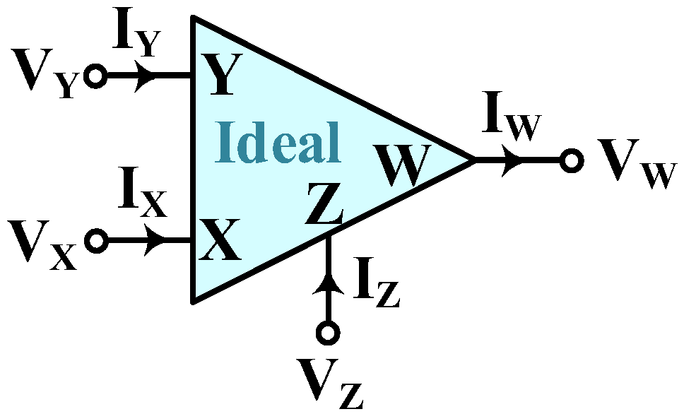
2. Circuit Descriptions and Realizations
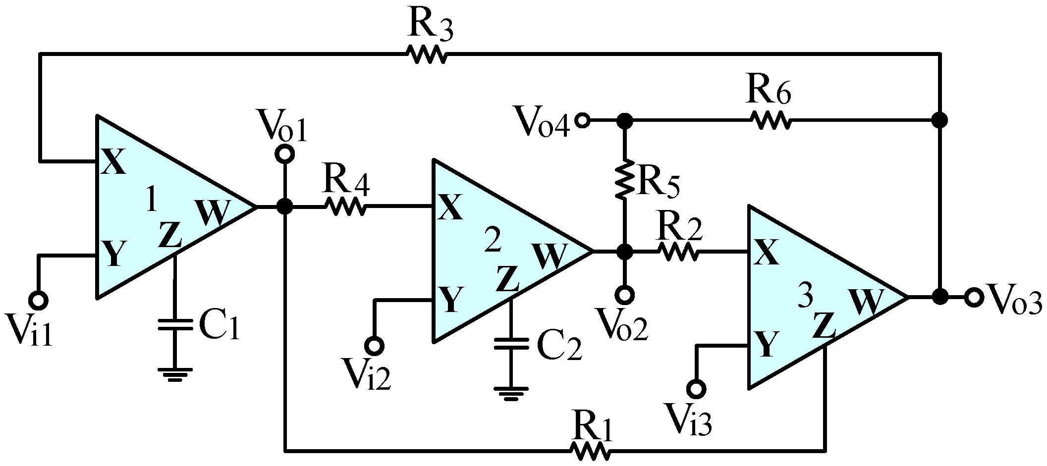
2.1. Proposed Voltage-Mode UAF Configuration
- (a)
- If R1 = R2 and R5 = R6, the regular BR filtering function with 1/2 passband gain can be realized in (12).
- (b)
- If R5 < R6 and ωz > ωo, the LPN filtering function can be obtained in (8).
- (c)
- If R5 > R6 and ωz < ωo, the HPN filtering function can also be obtained in (8).
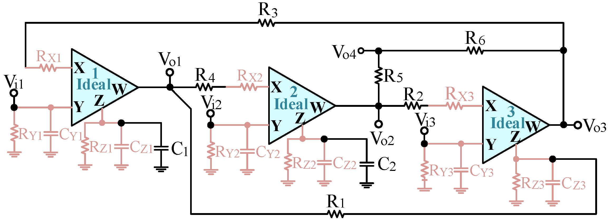
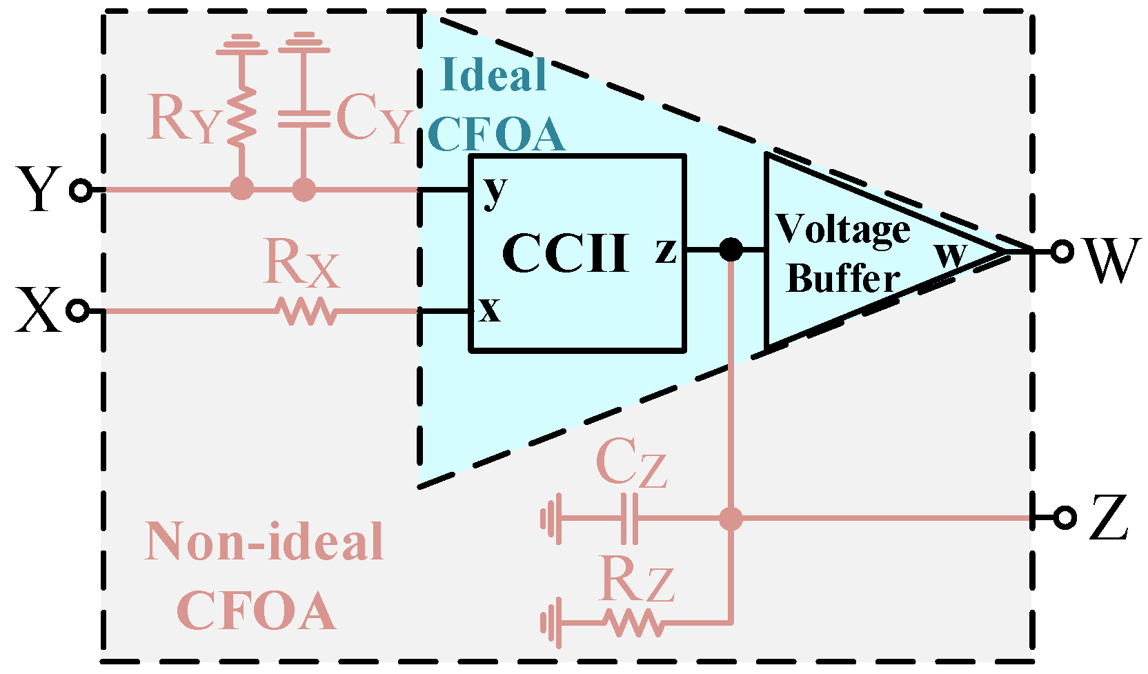
2.2. Effects of CFOA Non-Idealities on Voltage-Mode UAF Characteristics
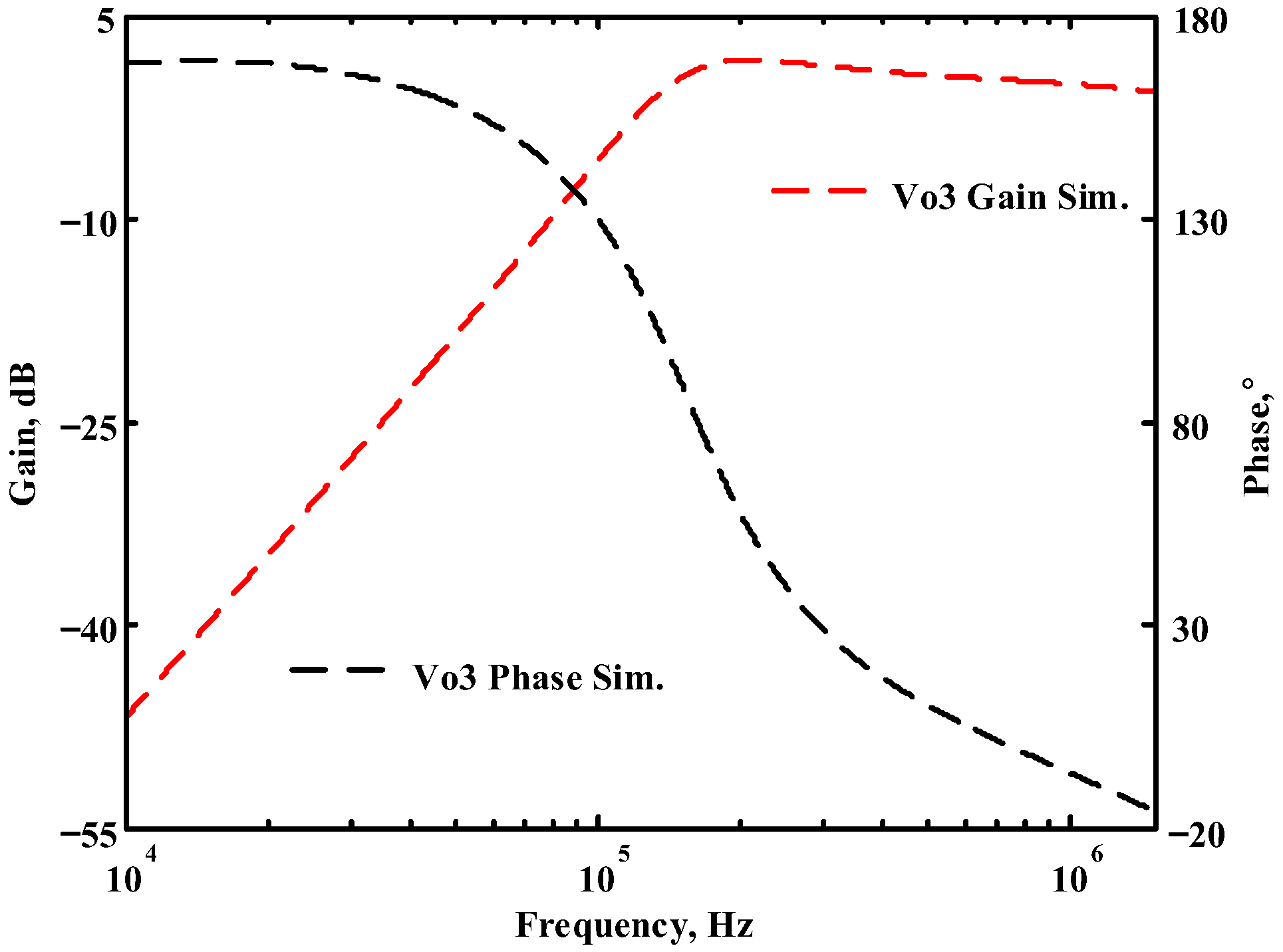
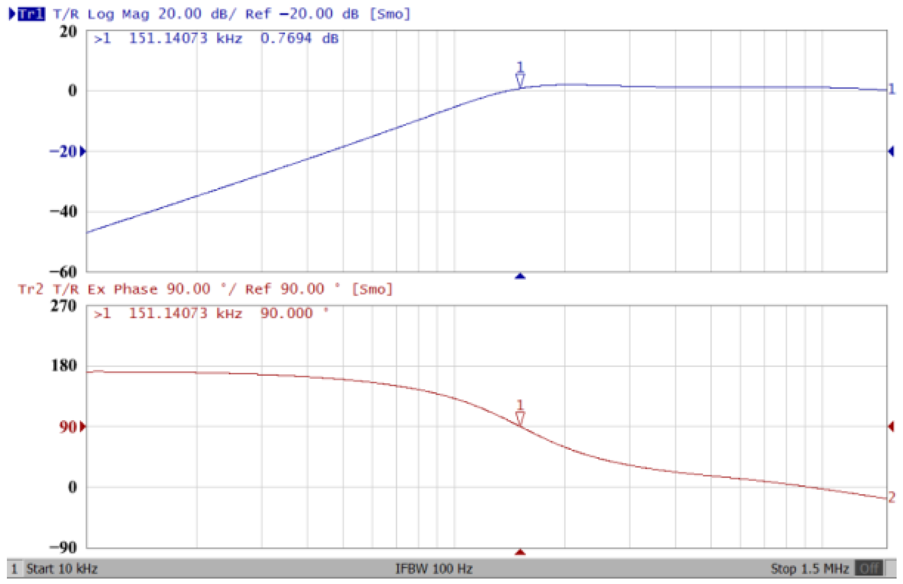
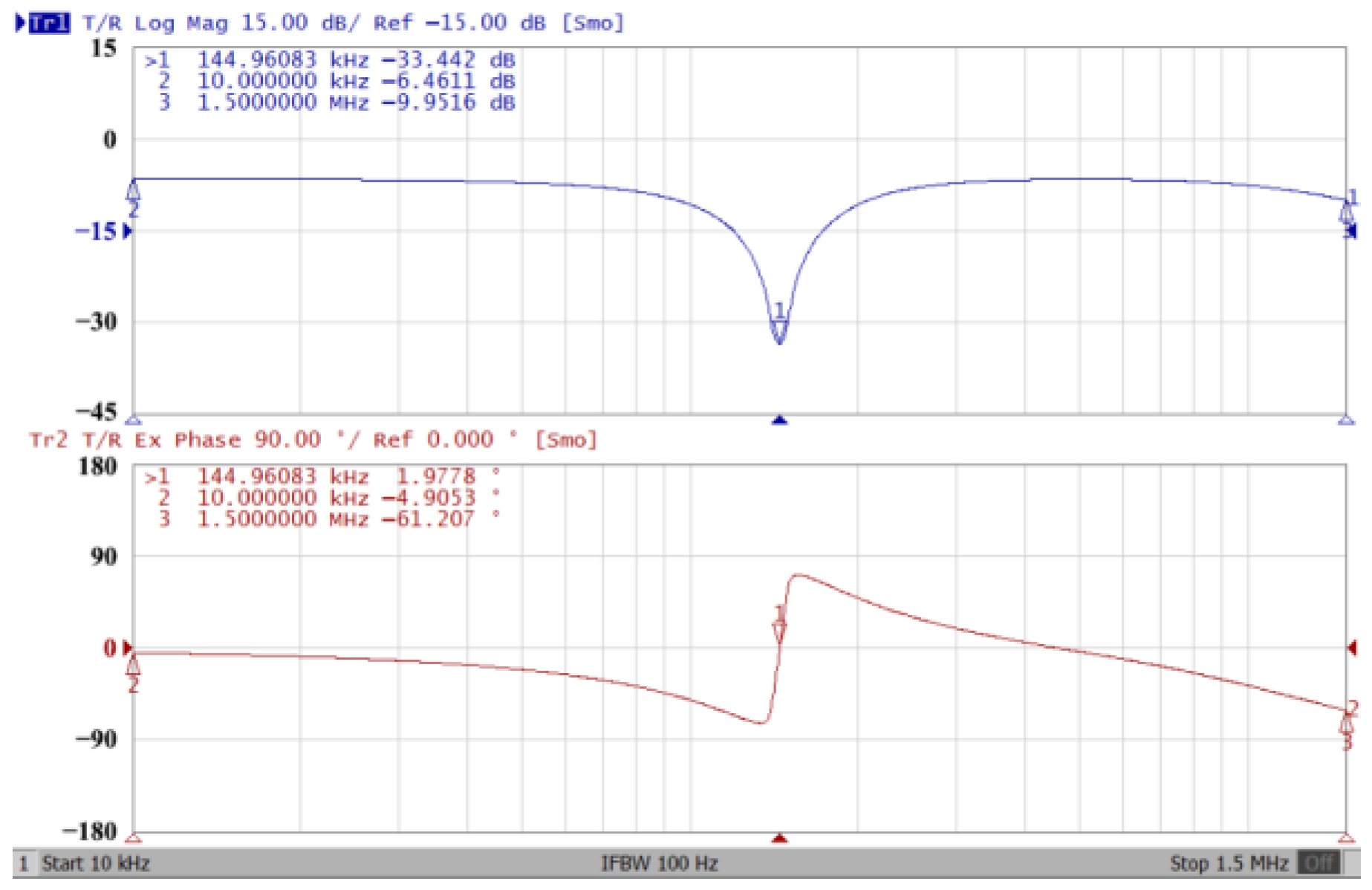
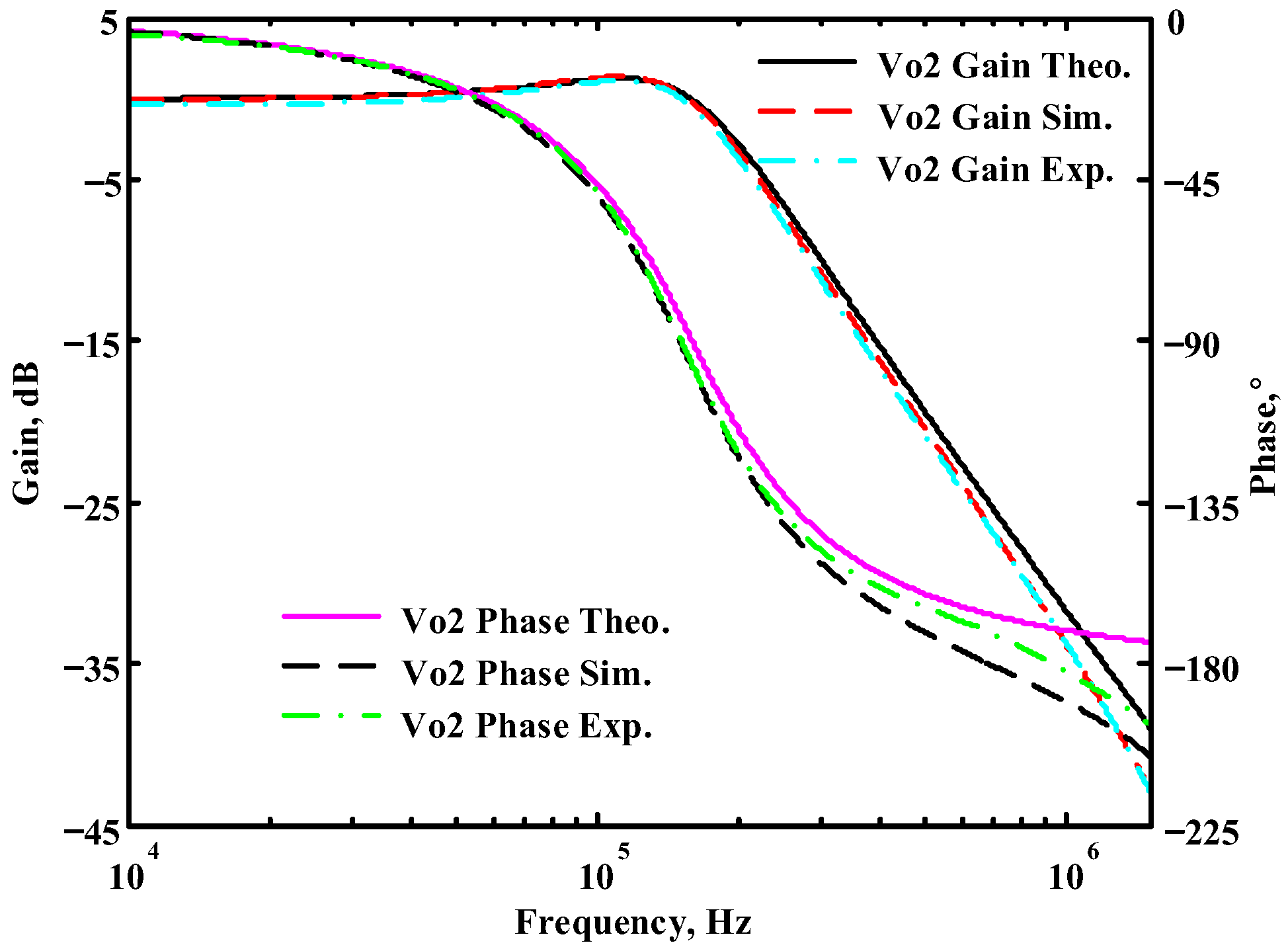
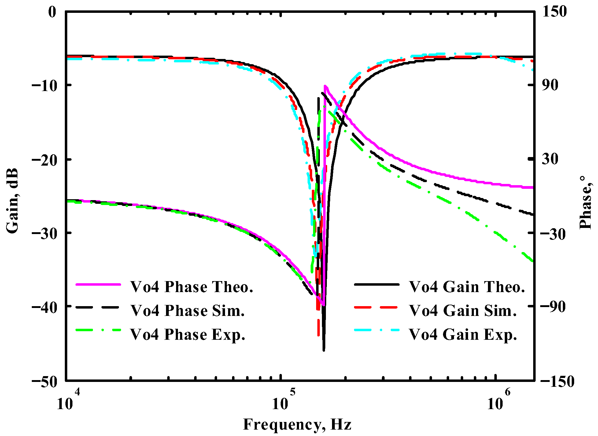
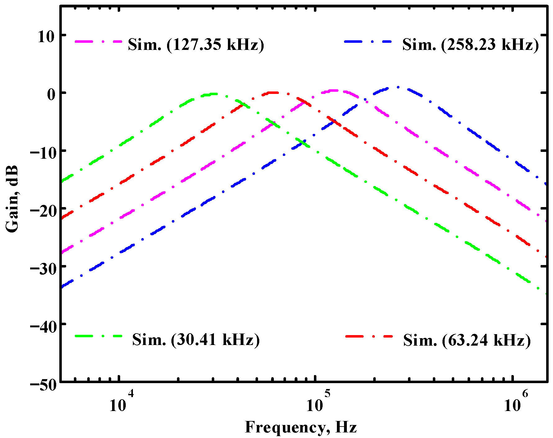
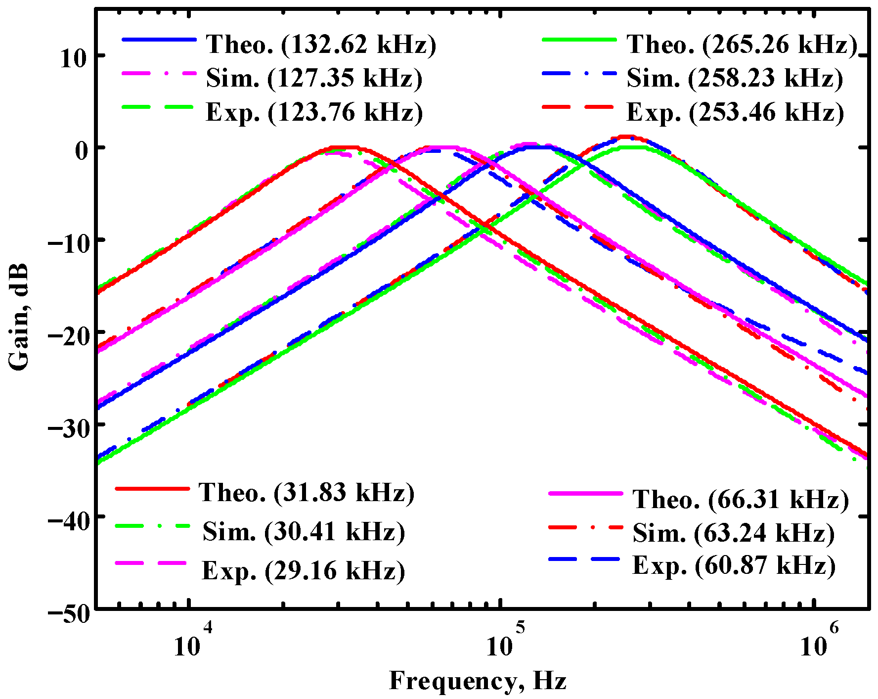
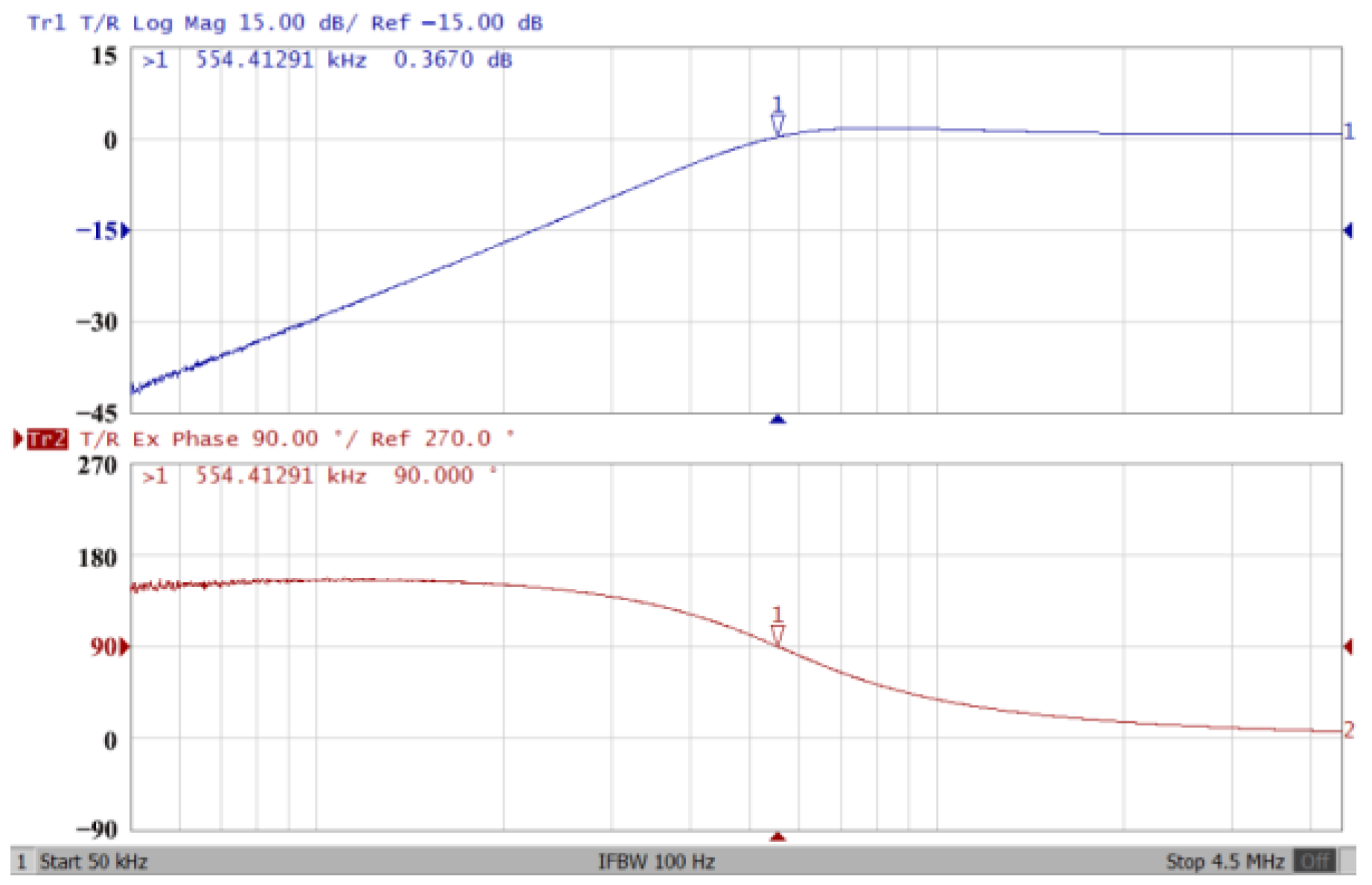
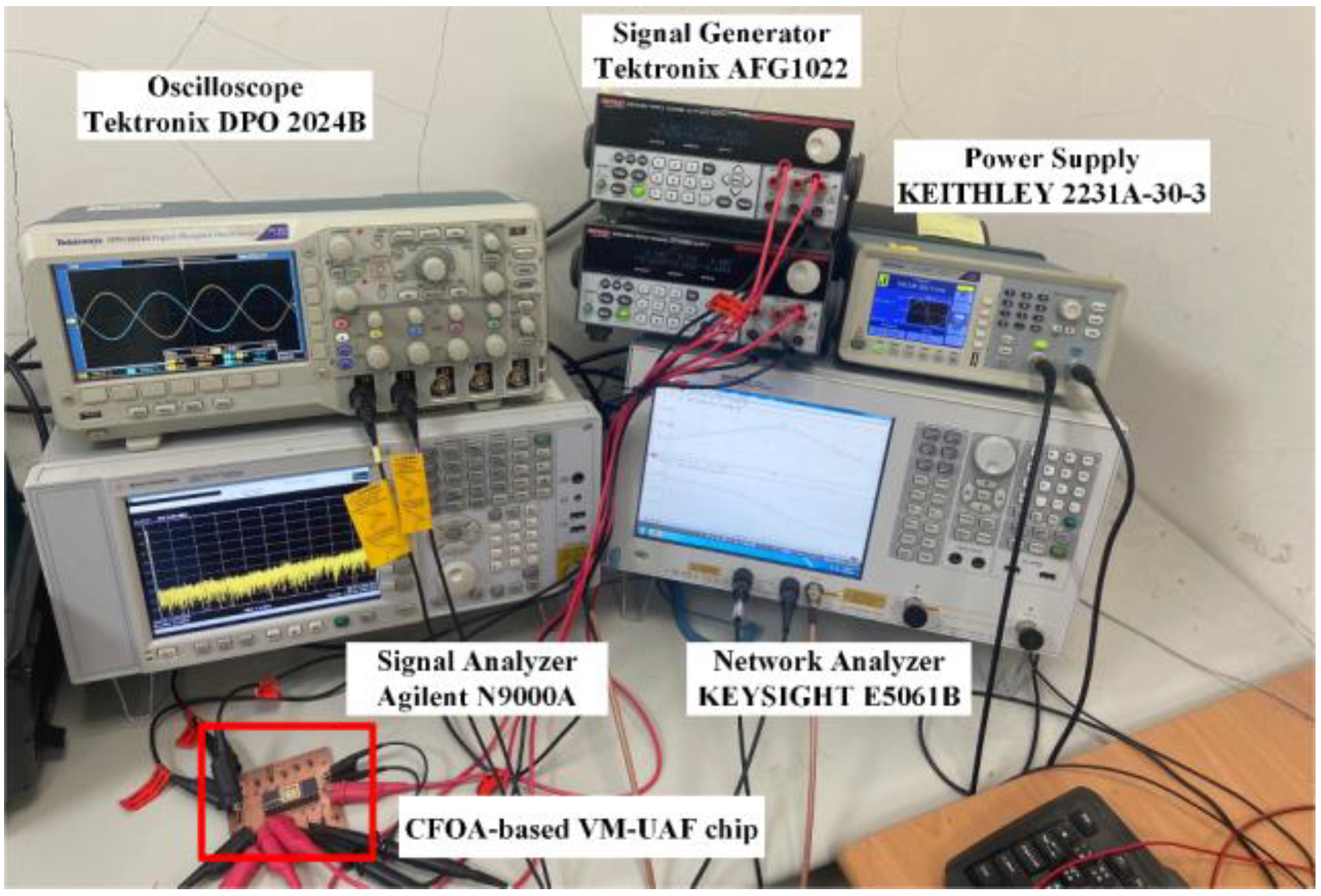
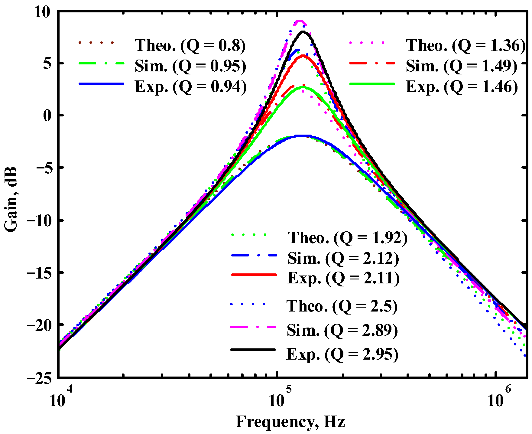
3. Simulation and Experimental Results
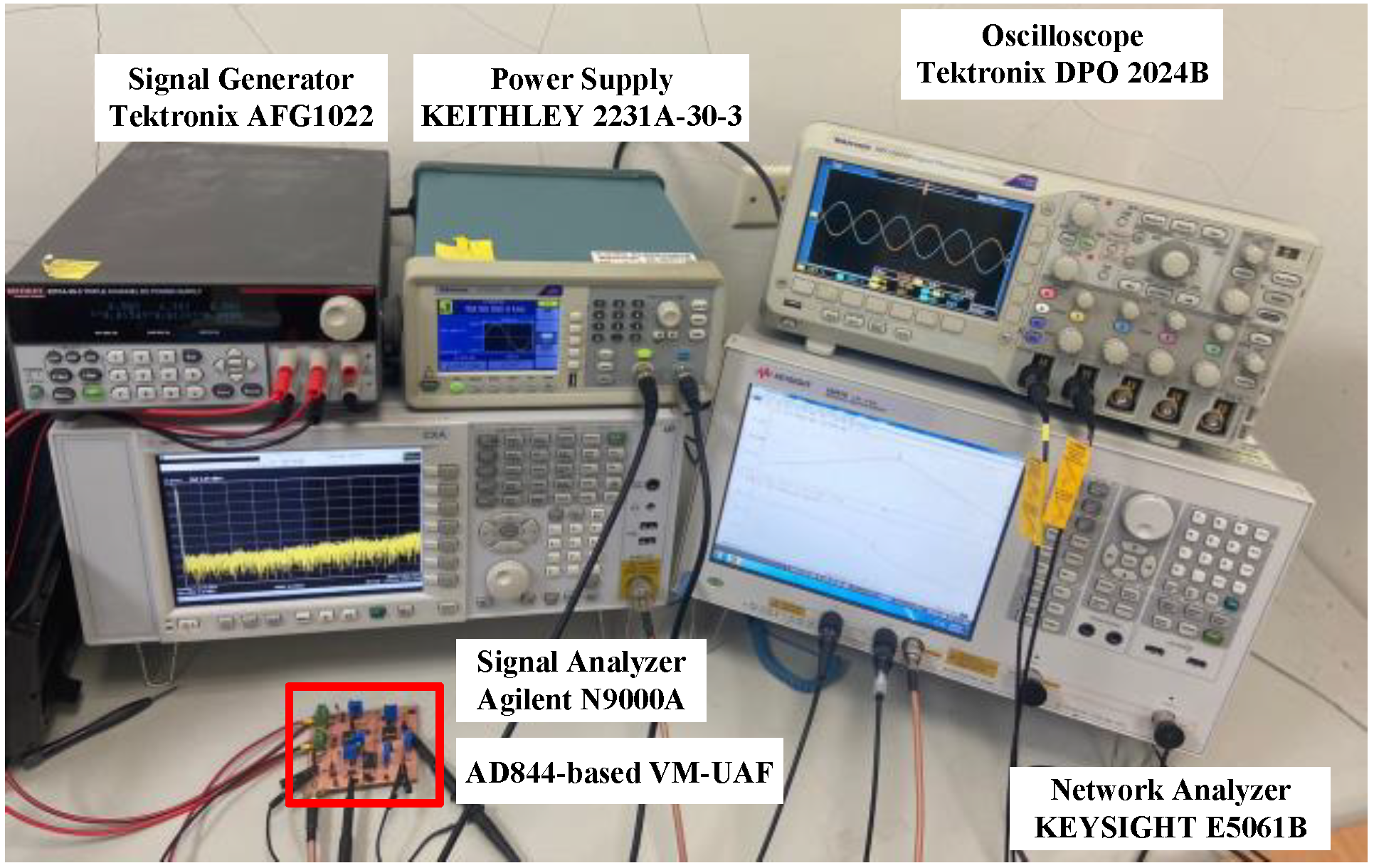
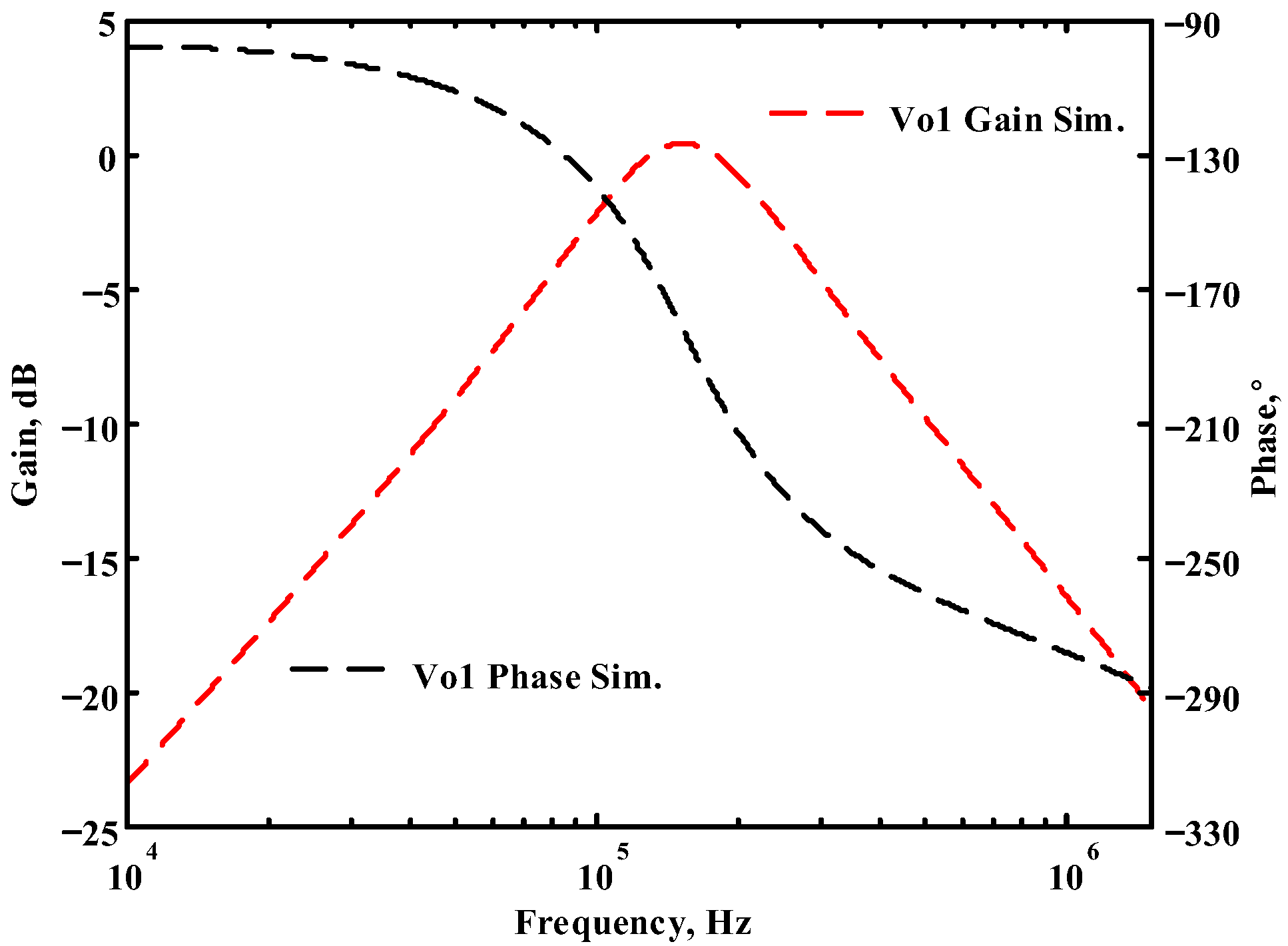
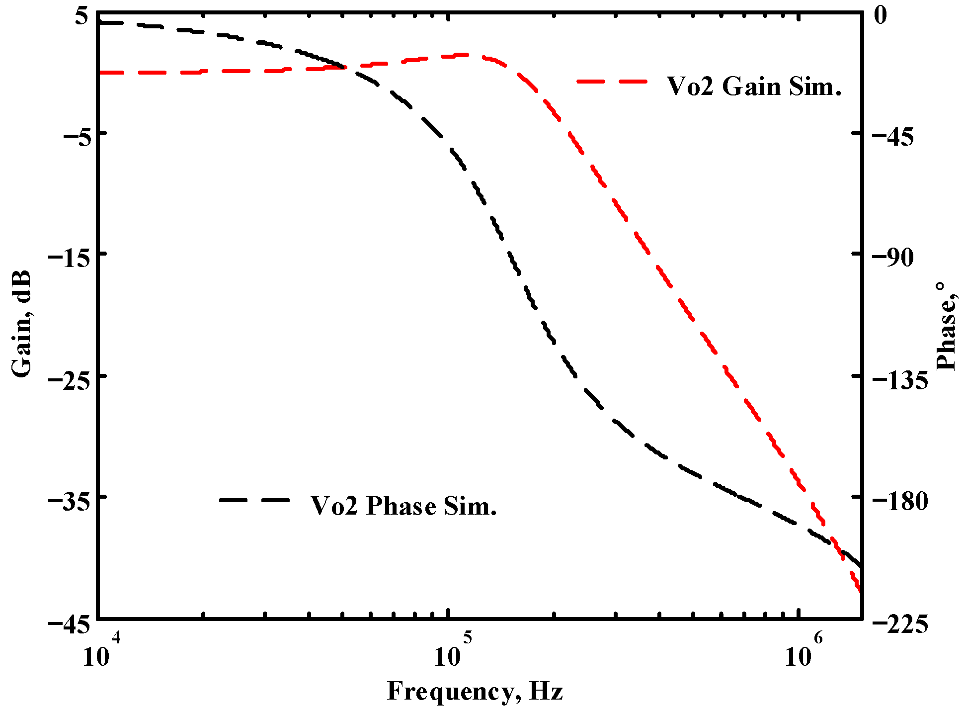
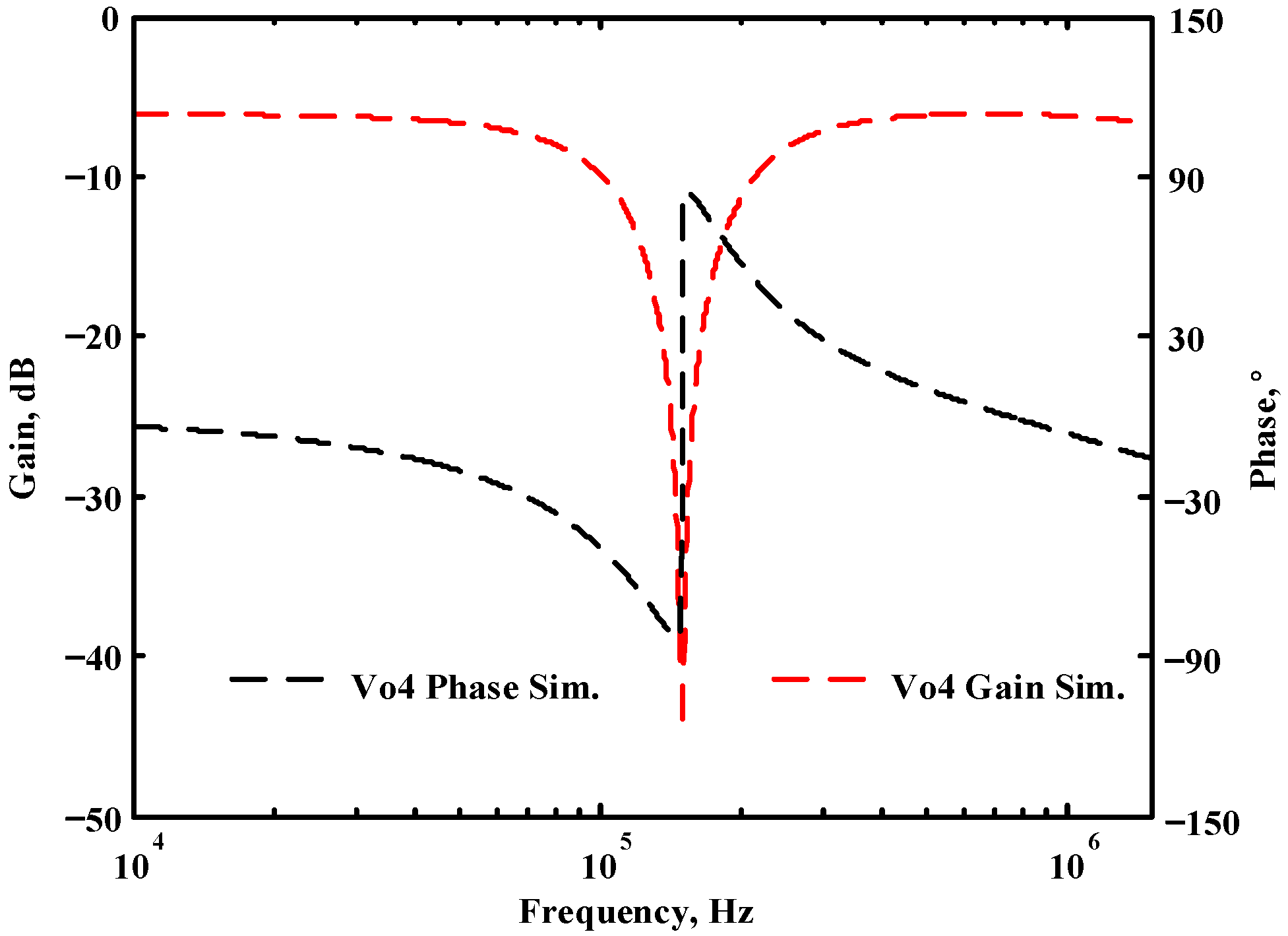
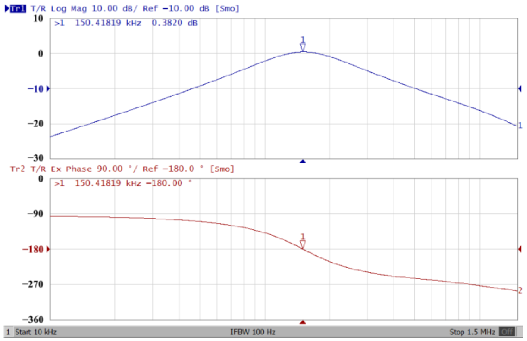
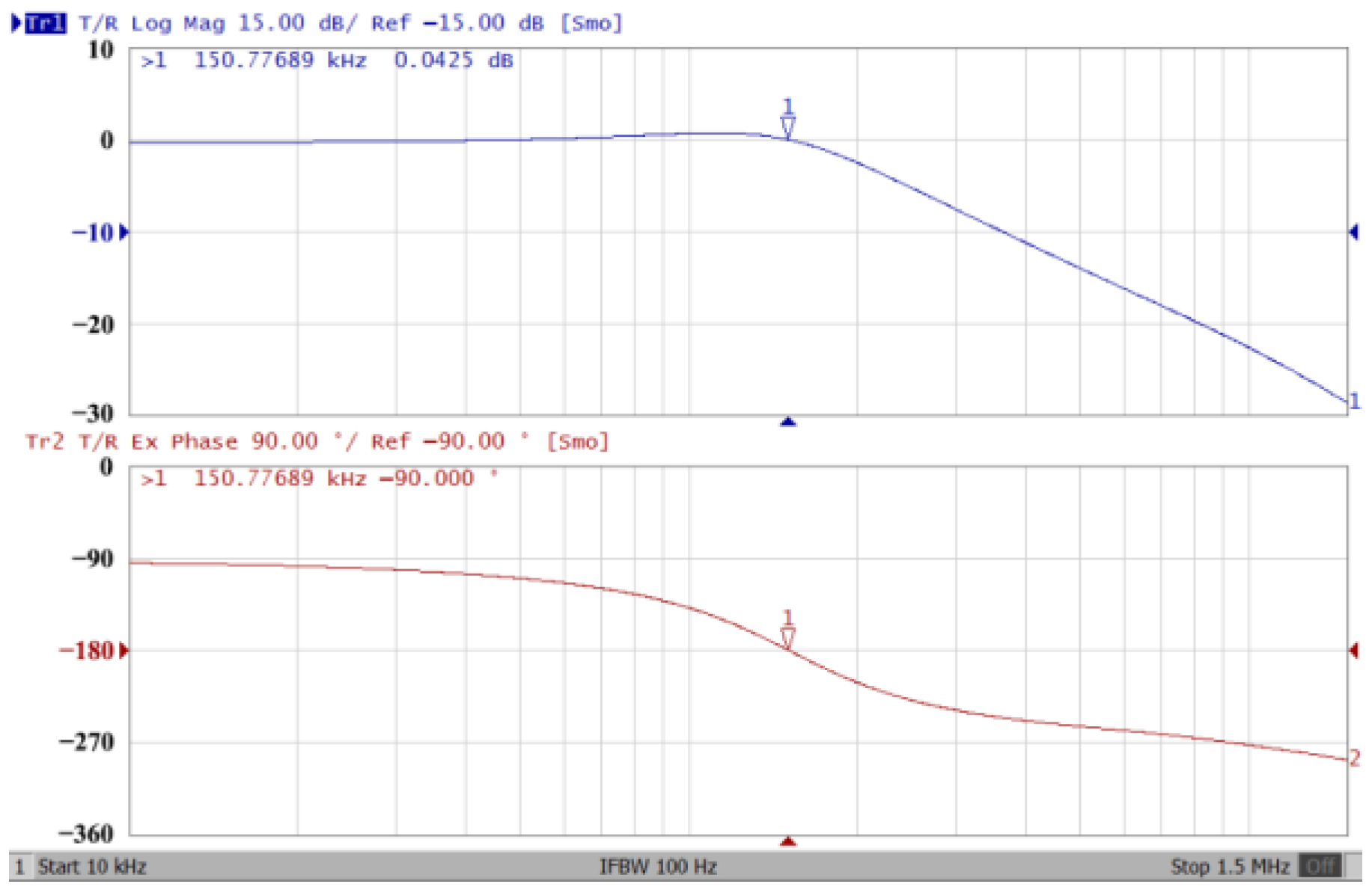
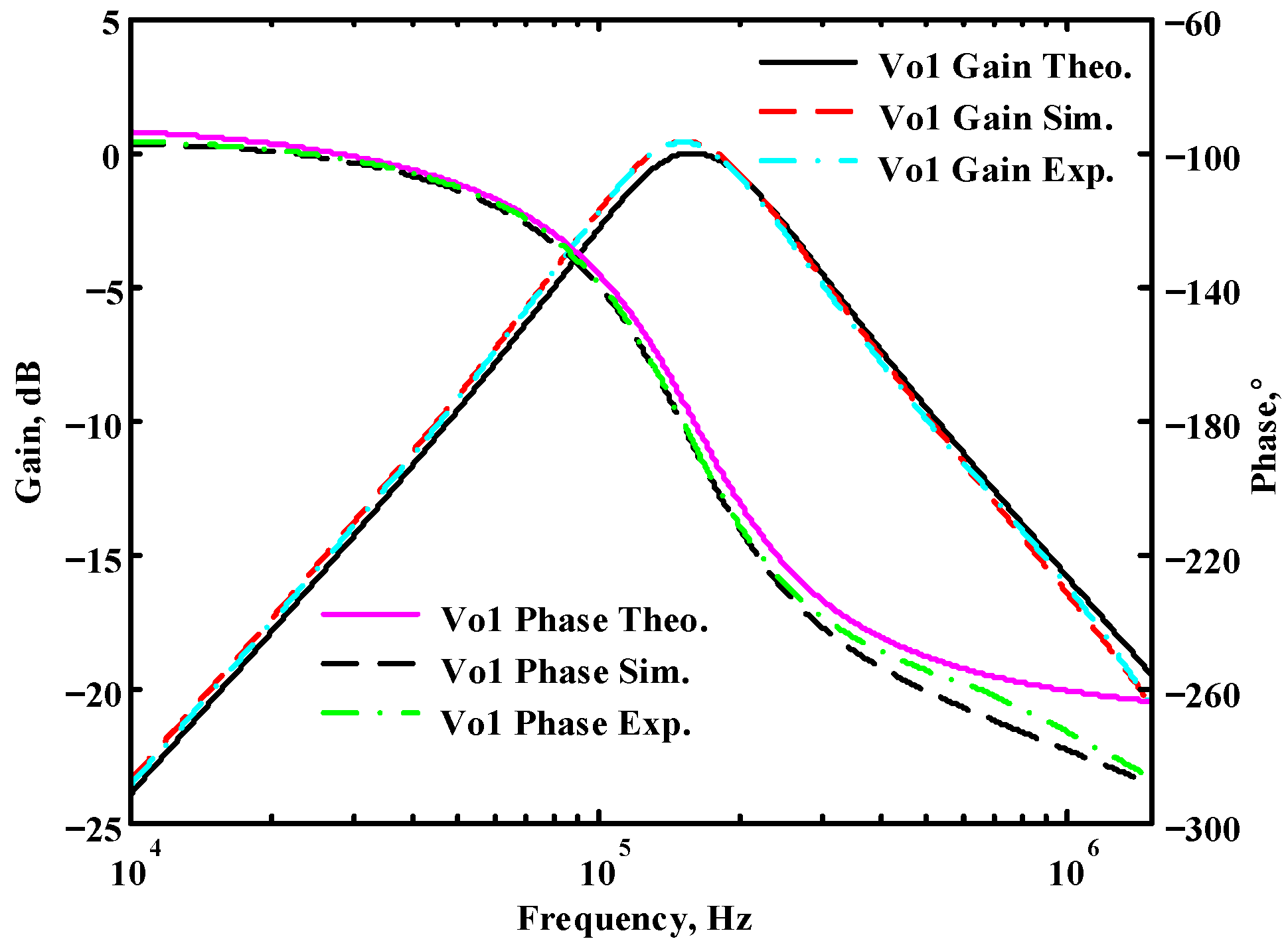
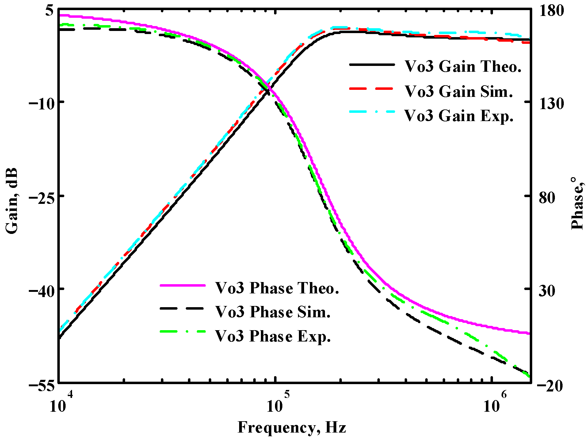
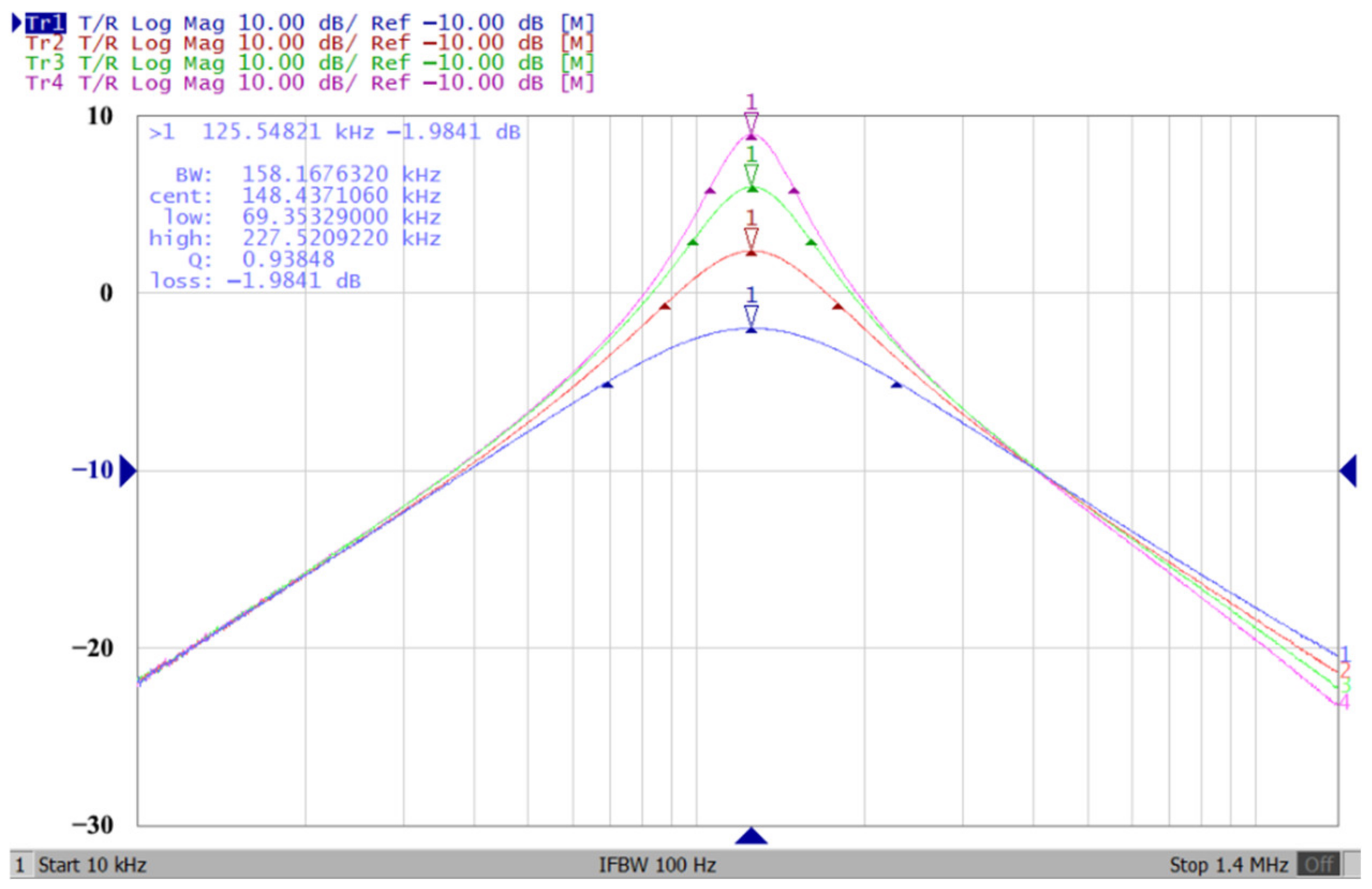
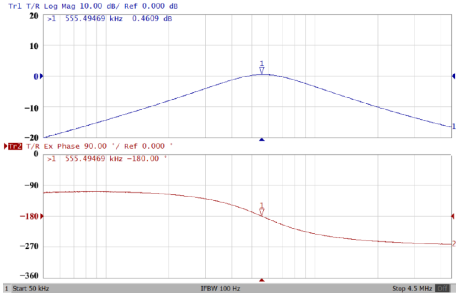
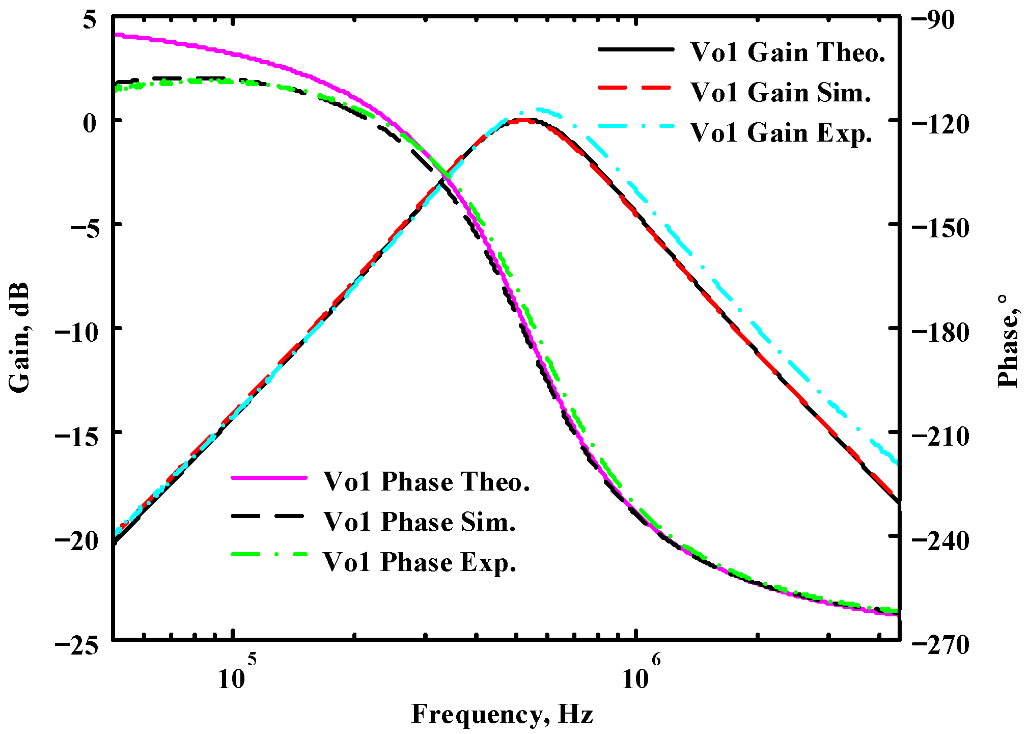
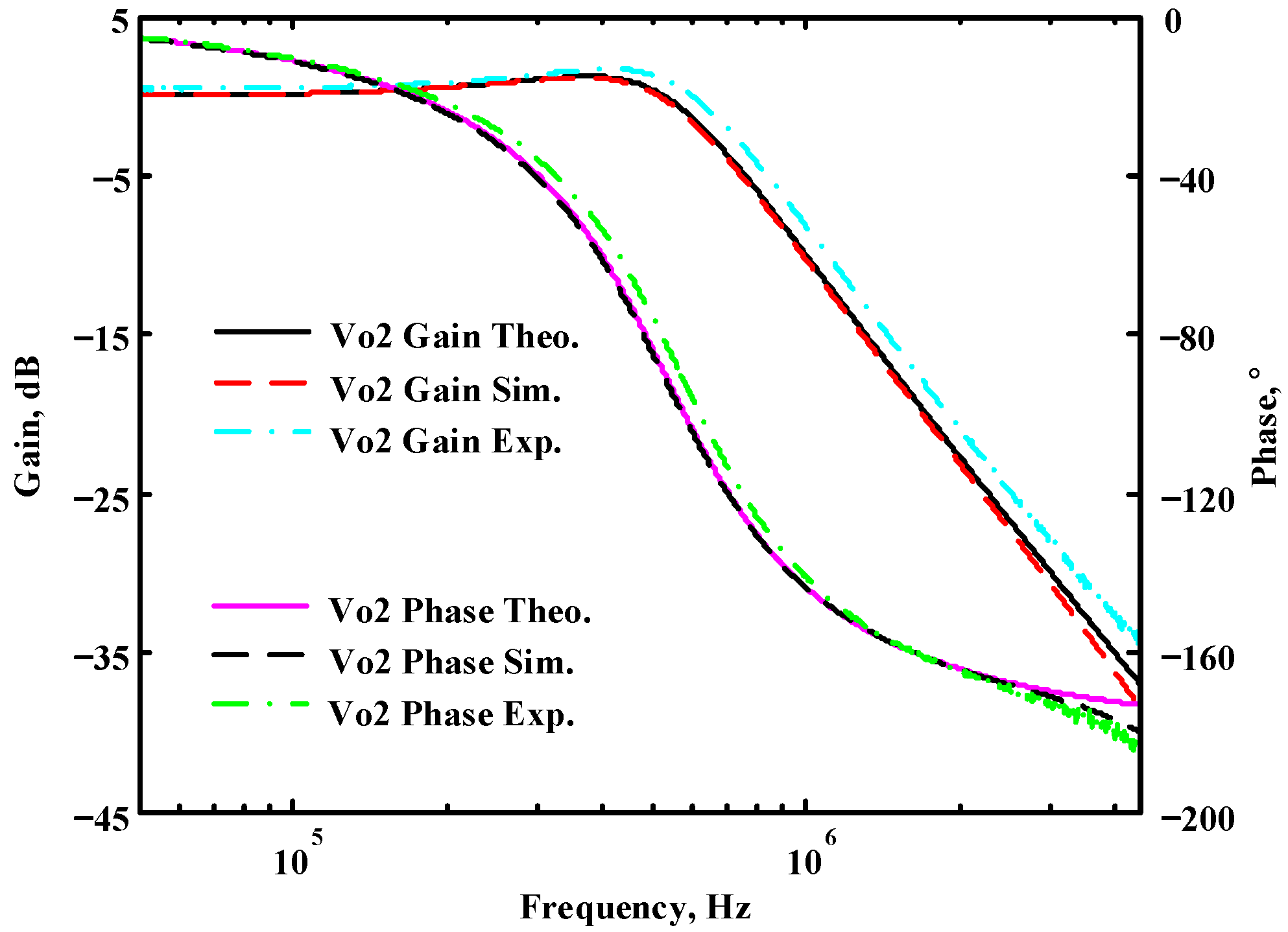
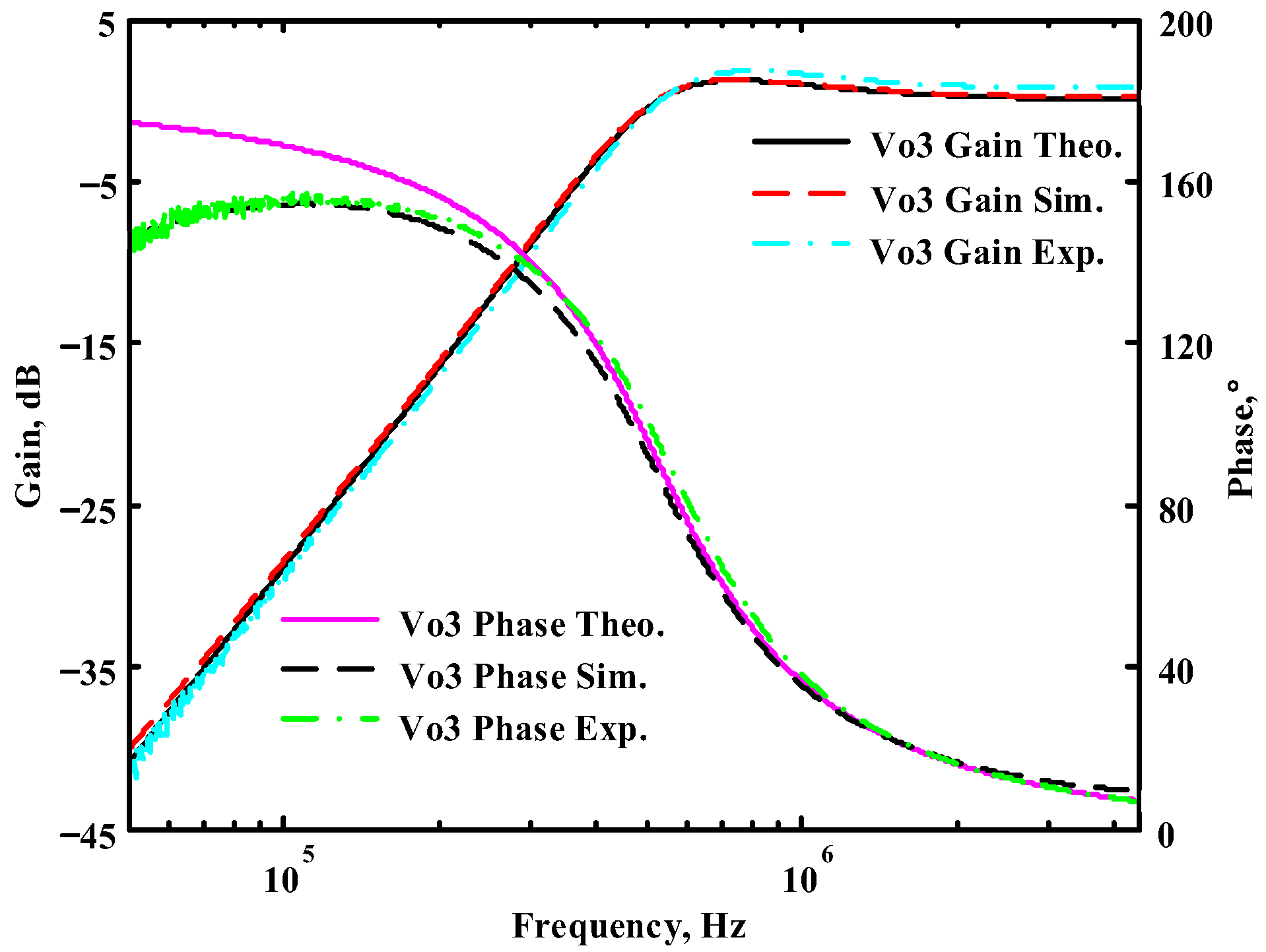
3.1. The AD844-Based Voltage-Mode UAF Simulation and Measurement Results
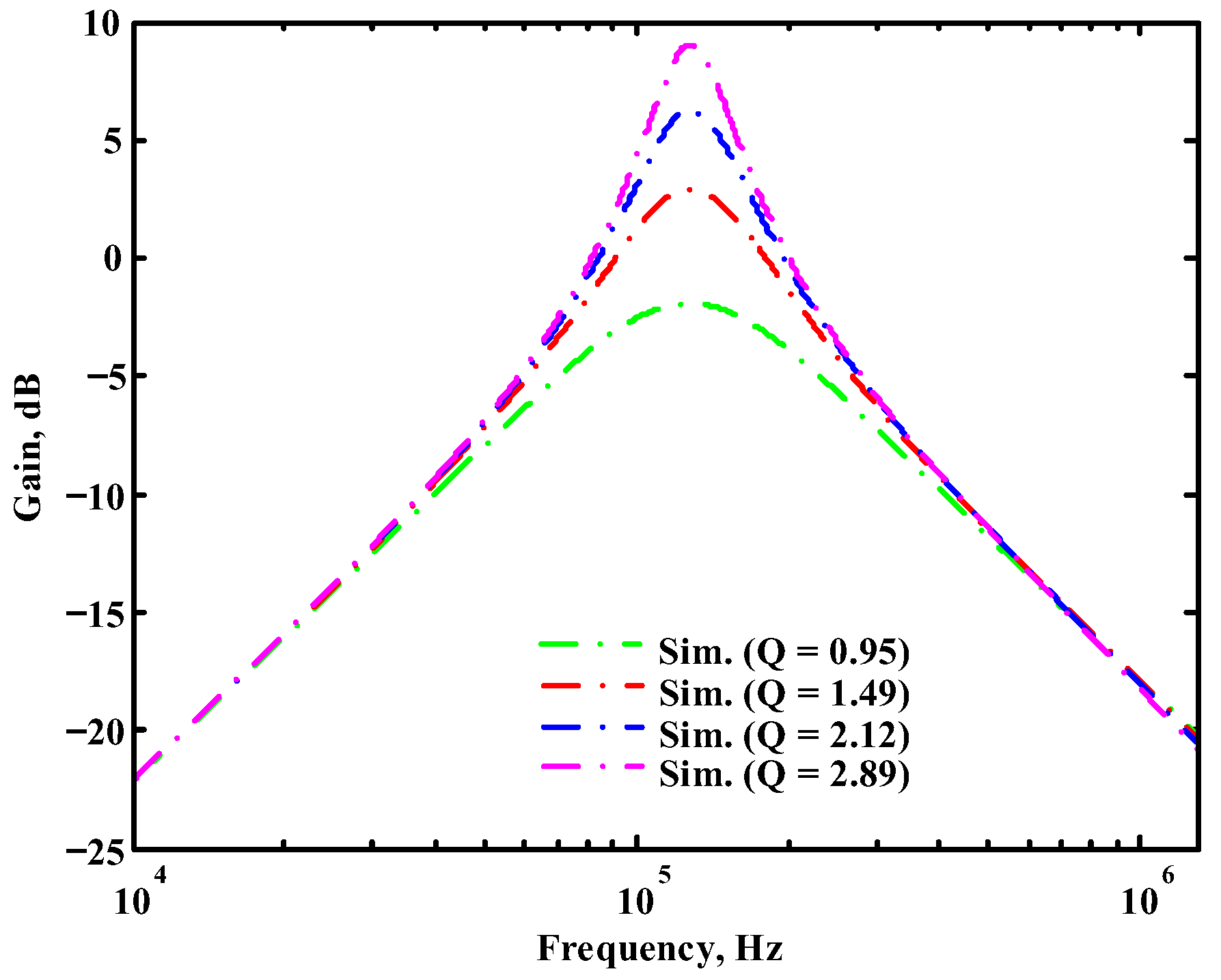
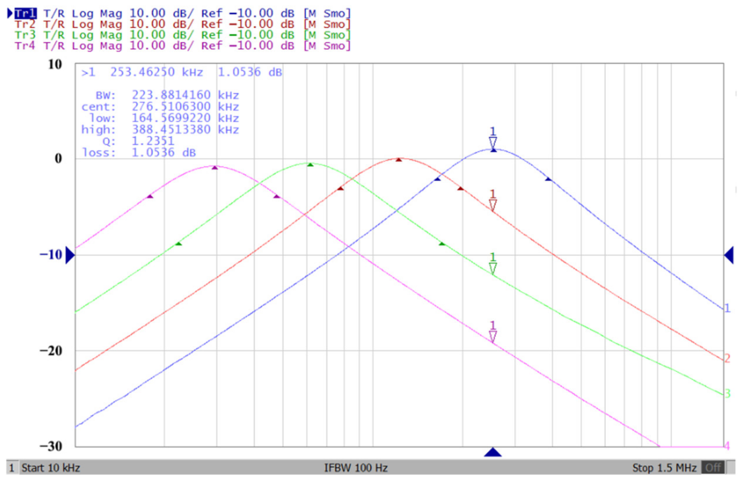
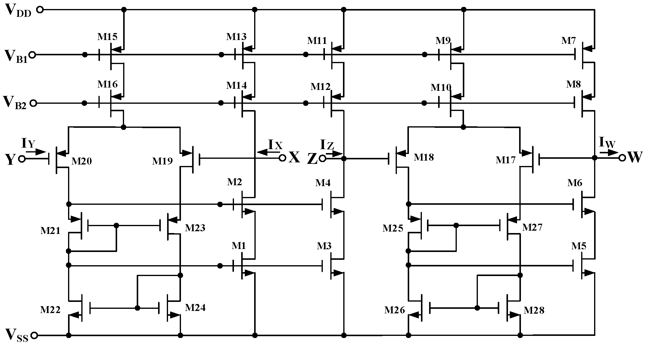
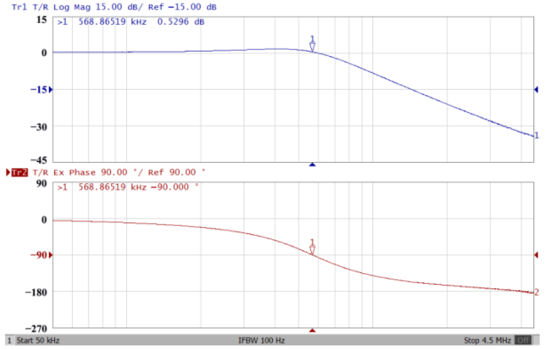
3.2. The On-Chip CMOS VM-UAF Simulation and Measurement Results
4. Conclusions
Author Contributions
Funding
Institutional Review Board Statement
Informed Consent Statement
Data Availability Statement
Conflicts of Interest
References
- Kumngern, M.; Aupithak, N.; Khateb, F.; Kulej, T. 0.5 V Fifth-order butterworth low-pass filter using multiple-input OTA for ECG applications. Sensors 2020, 20, 7343. [Google Scholar] [CrossRef]
- Tangsangiumvisai, N.; Chambers, J.A.; Constantinides, A.G. Higher-order time-varying allpass filters for signal decorrelation in stereophonic acoustic echo cancellation. Electron. Lett. 1999, 35, 88–90. [Google Scholar] [CrossRef]
- Chiu, W.Y.; Horng, J.W. High-input and low-output impedance voltage-mode universal biquadratic filter using DDCCs. IEEE Trans. Circuits Syst. II Exp. Briefs 2007, 54, 649–652. [Google Scholar] [CrossRef]
- Prommee, P.; Karawanich, K.; Khateb, F.; Kulej, T. Voltage-mode elliptic band-pass filter based on multiple-input transconductor. IEEE Access 2021, 9, 32582–32590. [Google Scholar] [CrossRef]
- Sotner, R.; Jerabek, J.; Polak, L.; Theumer, R.; Langhammer, L. Electronic tunability and cancellation of serial losses in wire coils. Sensors 2022, 22, 7373. [Google Scholar] [CrossRef]
- Zhao, Z.; Tong, H.; Deng, Y.; Xu, W.; Zhang, Y.; Ye, H. Single-lead fetal ECG extraction based on a parallel marginalized particle filter. Sensors 2017, 17, 1456. [Google Scholar] [CrossRef]
- Márquez, A.; Pérez-Bailón, J.; Calvo, B.; Medrano, N.; Martínez, P.A. A CMOS self-contained quadrature signal generator for SoC impedance spectroscopy. Sensors 2018, 18, 1382. [Google Scholar] [CrossRef] [PubMed]
- Yuce, E. Voltage-mode multifunction filters employing a single DVCC and grounded capacitors. IEEE Trans. Instrum. Meas. 2009, 58, 2216–2221. [Google Scholar] [CrossRef]
- Lee, C.N. Independently tunable plus-type DDCC-based voltage-mode universal biquad filter with MISO and SIMO types. Microelectron J. 2017, 67, 71–81. [Google Scholar] [CrossRef]
- Roongmuanpha, N.; Likhitkitwoerakul, N.; Fukuhara, M.; Tangsrirat, W. Single VDGA-based mixed-mode electronically tunable first-order universal filter. Sensors 2023, 23, 2759. [Google Scholar] [CrossRef]
- Akbari, M.; Hussein, S.M.; Hashim, Y.; Tang, K.T. An adjustable dual-output current mode MOSFET-only filter. IEEE Trans. Circuits Syst. II Exp. Briefs 2021, 68, 1817–1821. [Google Scholar] [CrossRef]
- Alpaslan, H.; Yuce, E. DVCC+ based multifunction and universal filters with the high input impedance features. Analog Integr. Circuits Signal Process. 2020, 103, 325–335. [Google Scholar] [CrossRef]
- Lee, C.N. Fully Cascadable mixed-mode universal filter biquad using DDCCs and grounded passive components. J. Circuits Syst. Comput. 2011, 20, 607–620. [Google Scholar] [CrossRef]
- Kumngern, M.; Khateb, F.; Kulej, T.; Psychalions, C. Multiple-input universal filter and quadrature oscillator using multiple-input operational transconductance amplifiers. IEEE Access 2021, 9, 56253–56263. [Google Scholar] [CrossRef]
- Khateb, F.; Kumngern, M.; Kulej, T.; Biolek, D. 0.5 V differential difference transconductance amplifier and its application in voltage-mode universal filter. IEEE Access 2022, 10, 43209–43220. [Google Scholar] [CrossRef]
- Fabre, A.; Saaid, O.; Barthelemy, H. On the frequency limitations of the circuits based on second generation current conveyors. Analog Integr. Circuits Signal Process. 1995, 7, 113–129. [Google Scholar] [CrossRef]
- Supavarasuwat, P.; Kumngern, M.; Sangyaem, S.; Jaikla, W.; Khateb, F. Cascadable independently and electronically tunable voltage-mode universal filter with grounded passive components. AEU Int. J. Electron. Commun. 2018, 84, 290–299. [Google Scholar] [CrossRef]
- Wai, M.P.P.; Suwanjan, P.; Jaikla, W.; Chaichana, A. Electronically and orthogonally tunable SITO voltage-mode multifunction biquad filter using LT1228s. Elektron. Ir Elektrotechnika 2021, 27, 11–17. [Google Scholar] [CrossRef]
- Schmid, H. Why “current mode” does not guarantee good performance. Analog Integr. Circuits Signal Process. 2003, 35, 79–90. [Google Scholar] [CrossRef]
- Liu, S.I.; Wu, D.S. New current-feedback amplifier-based universal biquadratic filter. IEEE Trans. Instrum. Meas. 1995, 44, 915–917. [Google Scholar]
- Soliman, A.M. A new filter configuration using current feedback op-amp. Microelectron. J. 1998, 29, 409–419. [Google Scholar] [CrossRef]
- Bhaskar, D.R. Realisation of second-order sinusoidal oscillator/filters with non-interacting controls using CFAs. Frequenz 2003, 57, 12–14. [Google Scholar] [CrossRef]
- Shan, N.A.; Rather, M.F.; Iqbal, S.Z. CFA-based three input and two outputs voltage-mode universal filter. Indian J. Pure Appl. Phy. 2005, 43, 636–639. [Google Scholar]
- Nikoloudis, S.; Psychalinos, C. Multiple input single output universal biquad filter with current feedback operational amplifiers. Circuits Syst. Signal Process. 2010, 29, 1167–1180. [Google Scholar] [CrossRef]
- Topaloglu, S.; Sagbas, M.; Anday, F. Three-input single-output second-order filters using current-feedback amplifiers. AEU Int. J. Electron. Commun. 2012, 66, 683–686. [Google Scholar] [CrossRef]
- Verma, R.; Pandey, N.; Pandey, R. CFOA based low pass and high pass fractional step filter realizations. AEU Int. J. Electron. Commun. 2019, 99, 61–76. [Google Scholar] [CrossRef]
- Chang, C.M.; Hwang, C.S.; Tu, S.H. Voltage-mode notch, lowpass and bandpass filter using current-feedback amplifiers. Electron. Lett. 1994, 30, 2022–2023. [Google Scholar] [CrossRef]
- Soliman, A.M. Applications of the current feedback operational amplifiers. Analog Integr. Circuits Signal Process. 1996, 11, 265–302. [Google Scholar] [CrossRef]
- Horng, J.W.; Lee, M.H. High input impedance voltage-mode lowpass, bandpass and highpass filter using current-feedback amplifiers. Electron. Lett. 1997, 33, 947–948. [Google Scholar] [CrossRef]
- Senani, R. Realization of a class of analog signal processing/signal generation circuits: Novel configurations using current feedback op-amps. Frequenz 1998, 52, 196–206. [Google Scholar] [CrossRef]
- Abuelma’atti, M.T.; Al-zaher, H.A. New universal filter with one input and five outputs using current-feedback amplifiers. Analog Integr. Circuits Signal Process. 1998, 16, 239–244. [Google Scholar] [CrossRef]
- Singh, A.K.; Senani, R. CFOA-based state-variable biquad and its high-frequency compensation. IEICE Electron. Express 2005, 2, 232–238. [Google Scholar] [CrossRef]
- Shah, N.A.; Iqbal, S.Z.; Rather, M.F. Versatile voltage-mode CFA-based universal filter. AEU Int. J. Electron. Commun. 2005, 59, 192–194. [Google Scholar] [CrossRef]
- Shan, N.A.; Malik, M.A. High input impedance voltage-mode lowpass, bandpass, highpass and notch filter using current feedback amplifiers. Indian J. Eng. Mater. Sci. 2005, 12, 278–280. [Google Scholar]
- Shan, N.A.; Malik, M.A. New high input impedance voltage-mode lowpass, bandpass and highpass filter using current feedback amplifiers. J. Circuits Sys. Comp. 2005, 14, 1037–1043. [Google Scholar]
- Singh, V.K.; Singh, A.K.; Bhaskar, D.R.; Senani, R. New universal biquads employing CFOAs. IEEE Trans. Circuits Syst. II Exp. Briefs 2006, 53, 1299–1303. [Google Scholar] [CrossRef]
- Wang, S.F.; Chen, H.P.; Ku, Y.; Chen, P.Y. A CFOA-based voltage-mode multifunction biquadratic filter and a quadrature oscillator using the CFOA-based biquadratic filter. Appl. Sci. 2019, 9, 2304. [Google Scholar] [CrossRef]
- Wang, S.F.; Chen, H.P.; Ku, Y.; Zhong, M.X. Voltage-mode multifunction biquad filter and its application as fully-uncoupled quadrature oscillator based on current-feedback operational amplifiers. Sensors 2020, 20, 6681. [Google Scholar] [CrossRef]
- Wang, S.F.; Chen, H.P.; Ku, Y.; Li, Y.F. High-input impedance voltage-mode multifunction filter. Appl. Sci. 2021, 11, 387. [Google Scholar] [CrossRef]
- Wang, S.F.; Chen, H.P.; Ku, Y.; Zhong, M.X. Analytical synthesis of high-pass, band-pass and low-pass biquadratic filters and its quadrature oscillator application using current-feedback operational amplifiers. IEEE Access 2021, 9, 13330–13343. [Google Scholar] [CrossRef]
- Chen, H.P.; Wang, S.F.; Ku, Y.; Yeh, A.C.; Chen, Y.H. Design of second-order multifunction filter IC based on current feedback amplifiers with independent voltage gain control. IEEE Access 2022, 10, 63301–63313. [Google Scholar] [CrossRef]
- Chen, H.P.; Wang, S.F.; Ku, Y.; Yi, Y.C.; Chen, Y.H. Experimental verification of on-chip biquadratic filter and oscillator. IEEE Sens. J. 2023, 23, 3736–3746. [Google Scholar] [CrossRef]
- Bhaskar, D.R.; Raj, A.; Senani, R. Three new CFOA-based SIMO-type universal active filter configurations with unrivalled features. AEU Int. J. Electron. Commun. 2022, 153, 154285. [Google Scholar] [CrossRef]
- AD844: 60 MHz, 2000 V/μs, Monolithic Op-amp with Quad Low Noise Data Sheet (Rev. G). May 2017. Available online: www.linear.com (accessed on 1 December 2020).


| Topology/Year | Number of Active and Passive Elements | Number of Filtering Functions | Simultaneous Realization of Filtering Functions | Use of Only Grounded Capacitors | No Series Capacitor on the X Terminal of the CFOA | No Switches Required | Orthogonal Control of Q and ωo | Operating Resonance Frequency fo | Measured Spurious-Free Dynamic Range | Measured Total Harmonic Distortion | Supply and Power | Results/ Technology |
|---|---|---|---|---|---|---|---|---|---|---|---|---|
| [32]/2005 | CFOA × 4 R × 6 C × 2 | 3 (LP, BP, HP) | LP, BP, HP | Yes | Yes | Yes | Yes | 15.9 kHz | NA | NA | NA | Sim./AD844 |
| [33]/2005 | CFOA × 3 R × 3 C × 2 | 5 (LP, BP, HP, BR, AP) | BP, HP, BR | No | Yes | Yes | Yes | 15.92 kHz | NA | NA | NA | Sim./AD844 |
| [34]/2005 | CFOA × 4 R × 4 C × 2 | 4 (LP, BP, HP, BR) | LP, BP, HP, BR | Yes | Yes | Yes | Yes | 7.96 kHz | NA | NA | NA | Exp./AD844 |
| [35]/2005 | CFOA × 3 R × 4 C × 2 | 3 (LP, BP, HP) | LP, BP, HP | Yes | No | Yes | No | 5.68 kHz | NA | NA | ±12 V | Sim./AD844 |
| [36] in Figure 1d/2006 | CFOA × 4 R × 8 C × 2 Switch × 1 | 5 (LP, BP, HP, BR, AP) | LP, BP, HP, BR/AP | Yes | Yes | No | No | 5.62 kHz | NA | NA | ±12 V | Exp./AD844 |
| [37]/2019 | CFOA × 3 R × 3 C × 2 | 4 (LP, BP, HP, BR) | LP, BP, BR | Yes | Yes | Yes | Yes | 39.79 kHz | NA | 0.56% @ 2 Vpp | ±6 V, 180 mW | Exp./AD844 |
| [38]/2020 | CFOA × 3 R × 4 C × 2 | 3 (LP, BP, BR) | LP, BP, BR | Yes | Yes | Yes | Yes | 102 kHz | NA | NA | ±6 V, 168 mW | Exp./AD844 |
| [39]/2021 | CFOA × 3 R × 3 C × 2 | 3 (LP, BP, BR) | LP, BP, BR | Yes | Yes | Yes | Yes | 39.79 kHz | NA | NA | ±6 V, 255 mW | Exp./AD844 |
| [40]/2021 | CFOA × 3 R × 4 C × 2 | 4 (LP, BP, HP, BR) | LP, BP, HP | Yes | Yes | Yes | Yes | 117.9 kHz (for the AD844) 757.88 kHz (for the chip) | NA | 3.2% @ 5.68 Vpp (for the AD844) 3.18% @ 1.2 Vpp (for the chip) | ±6 V, 168 mW (for the AD844) ±0.9 V, 5.4 mW (for the chip) | Exp./AD844 & Chip (TSMC 180 nm) |
| [41]/2022 | CFOA × 3 R × 4 C × 2 | 3 (LP, BP, BR) | LP, BP, BR | Yes | Yes | Yes | Yes | 568 kHz | 31.63 dBc | 3.3% @ 1.2 Vpp | ±0.9 V, 5.4 mW | Exp./Chip (TSMC 180 nm) |
| [42]/2023 | CFOA × 3 R × 5 C × 2 | 3 (LP, BP, BR) | LP, BP, BR | Yes | Yes | Yes | Yes | 530 kHz | 33.74 dBc | 2.88% @ 1.5 Vpp | ±0.9 V, 5.4 mW | Exp./Chip (TSMC 180 nm) |
| [43] in Figure 1a/2022 | CFOA × 4 R × 5 C × 2 Switch × 2 | 5 (LP, BP, HP, BR, AP) | LP, BP, BR, HP/AP | Yes | Yes | No | Yes | 159 kHz | NA | NA | ±10 V | Exp./AD844 |
| [43] in Figure 1b/2022 | CFOA × 4 R × 6 C × 2 Switch × 2 | 5 (LP, BP, HP, BR, AP) | LP, BP, BR, HP/AP | Yes | Yes | No | Yes | 159 kHz | NA | NA | ±10 V | Exp./AD844 |
| [43] in Figure 1 c/2022 | CFOA × 4 R × 6 C × 2 Switch × 1 | 5 (LP, BP, HP, BR, AP) | LP, BP, BR, HP/AP | Yes | Yes | No | Yes | 159 kHz | NA | NA | ±10 V | Exp./AD844 |
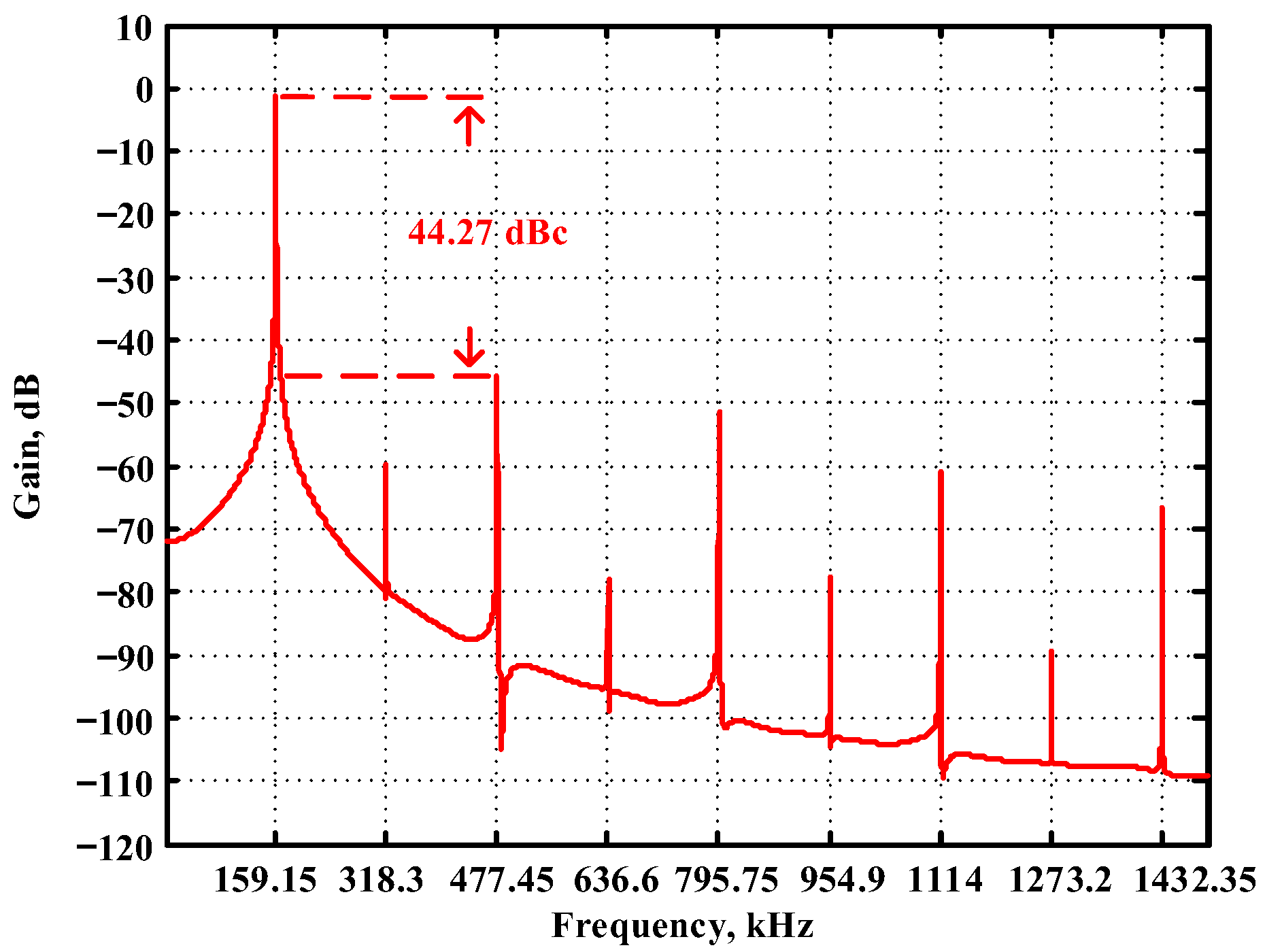
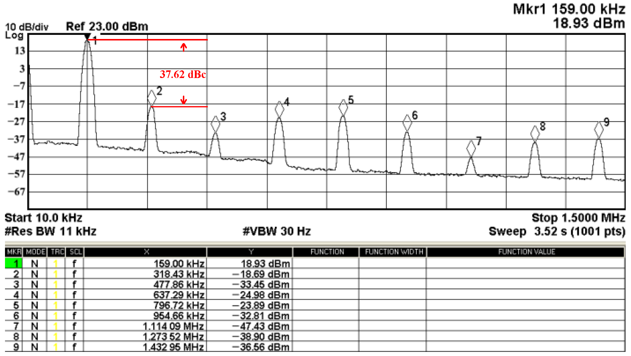
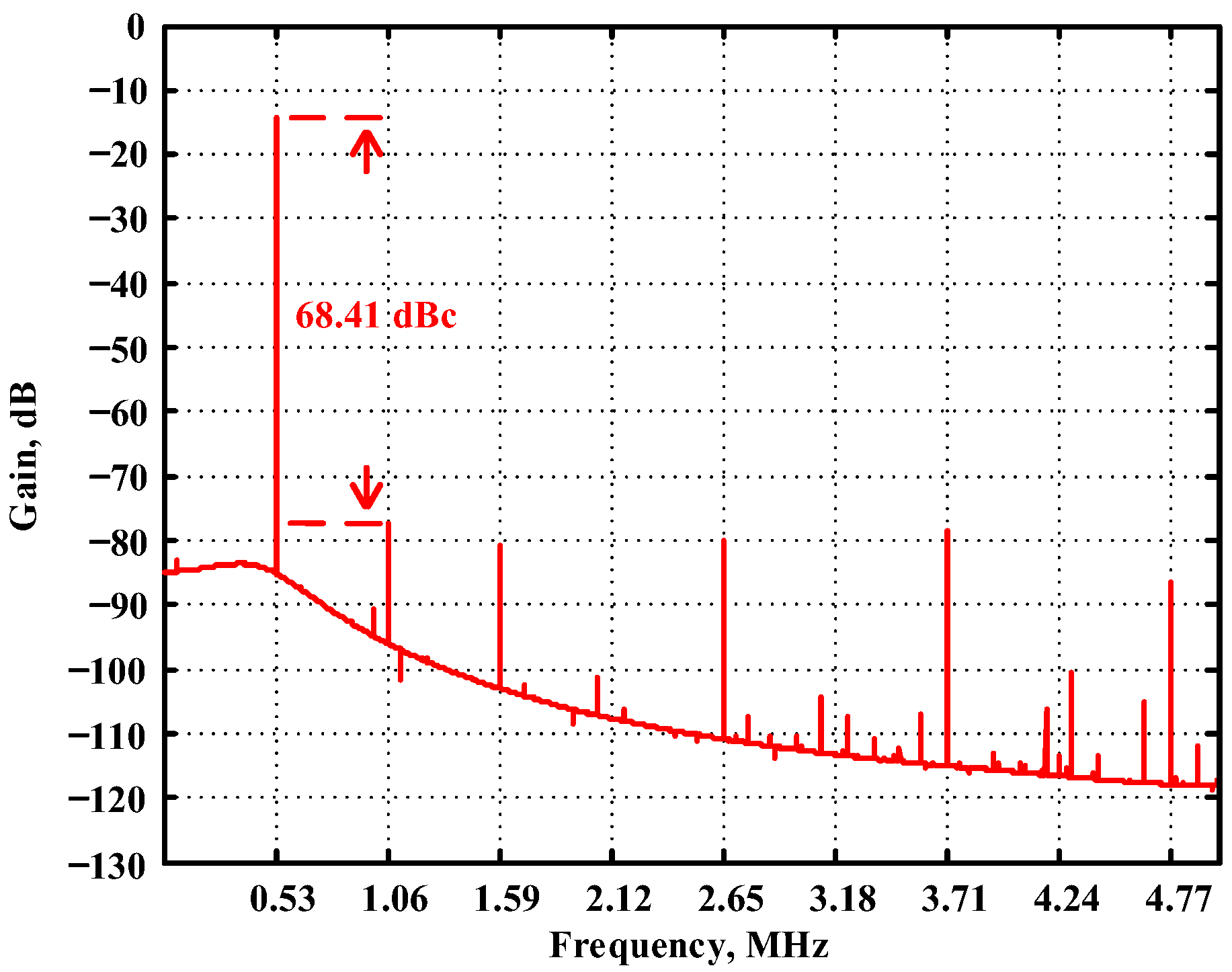
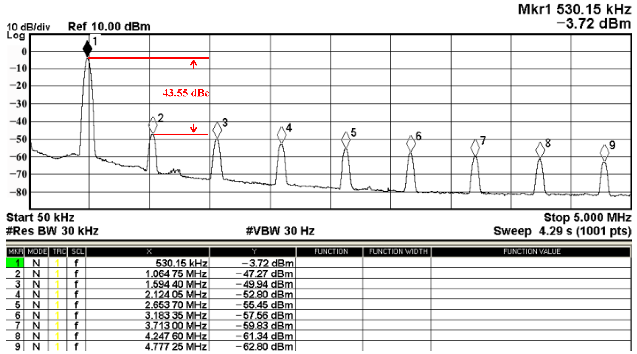
| Proposed | CFOA × 3 R × 6 C × 2 | 7 (LP, BP, HP, BR, LPN, HPN, AP) | LP, BP, HP, BR/ LPN/ HPN | Yes | Yes | Yes | Yes | 159.15 kHz (for the AD844) 530.5 kHz (for the chip) | 37.62 dBc (for the AD844) 43.55 dBc (for the chip) | 1.68% @ 5.2 Vpp (for the AD844) 1% @ 0.4 Vpp (for the chip) | ±6 V, 168 mW (for the AD844) ±0.9 V, 3.6 mW (for the chip) | Exp./AD844 & Chip (TSMC 180 nm) |
Disclaimer/Publisher’s Note: The statements, opinions and data contained in all publications are solely those of the individual author(s) and contributor(s) and not of MDPI and/or the editor(s). MDPI and/or the editor(s) disclaim responsibility for any injury to people or property resulting from any ideas, methods, instructions or products referred to in the content. |
© 2023 by the authors. Licensee MDPI, Basel, Switzerland. This article is an open access article distributed under the terms and conditions of the Creative Commons Attribution (CC BY) license (https://creativecommons.org/licenses/by/4.0/).
Share and Cite
Chen, H.-P.; Wey, I.-C.; Chen, L.-Y.; Wu, C.-Y.; Wang, S.-F. Design and Verification of a New Universal Active Filter Based on the Current Feedback Operational Amplifier and Commercial AD844 Integrated Circuit. Sensors 2023, 23, 8258. https://doi.org/10.3390/s23198258
Chen H-P, Wey I-C, Chen L-Y, Wu C-Y, Wang S-F. Design and Verification of a New Universal Active Filter Based on the Current Feedback Operational Amplifier and Commercial AD844 Integrated Circuit. Sensors. 2023; 23(19):8258. https://doi.org/10.3390/s23198258
Chicago/Turabian StyleChen, Hua-Pin, I-Chyn Wey, Liang-Yen Chen, Cheng-Yueh Wu, and San-Fu Wang. 2023. "Design and Verification of a New Universal Active Filter Based on the Current Feedback Operational Amplifier and Commercial AD844 Integrated Circuit" Sensors 23, no. 19: 8258. https://doi.org/10.3390/s23198258
APA StyleChen, H.-P., Wey, I.-C., Chen, L.-Y., Wu, C.-Y., & Wang, S.-F. (2023). Design and Verification of a New Universal Active Filter Based on the Current Feedback Operational Amplifier and Commercial AD844 Integrated Circuit. Sensors, 23(19), 8258. https://doi.org/10.3390/s23198258