
Exploring the Interpad Gap Region in Ultra-Fast Silicon Detectors: Insights into Isolation Structure and Electric Field Effects on Charge Multiplication
 , , and
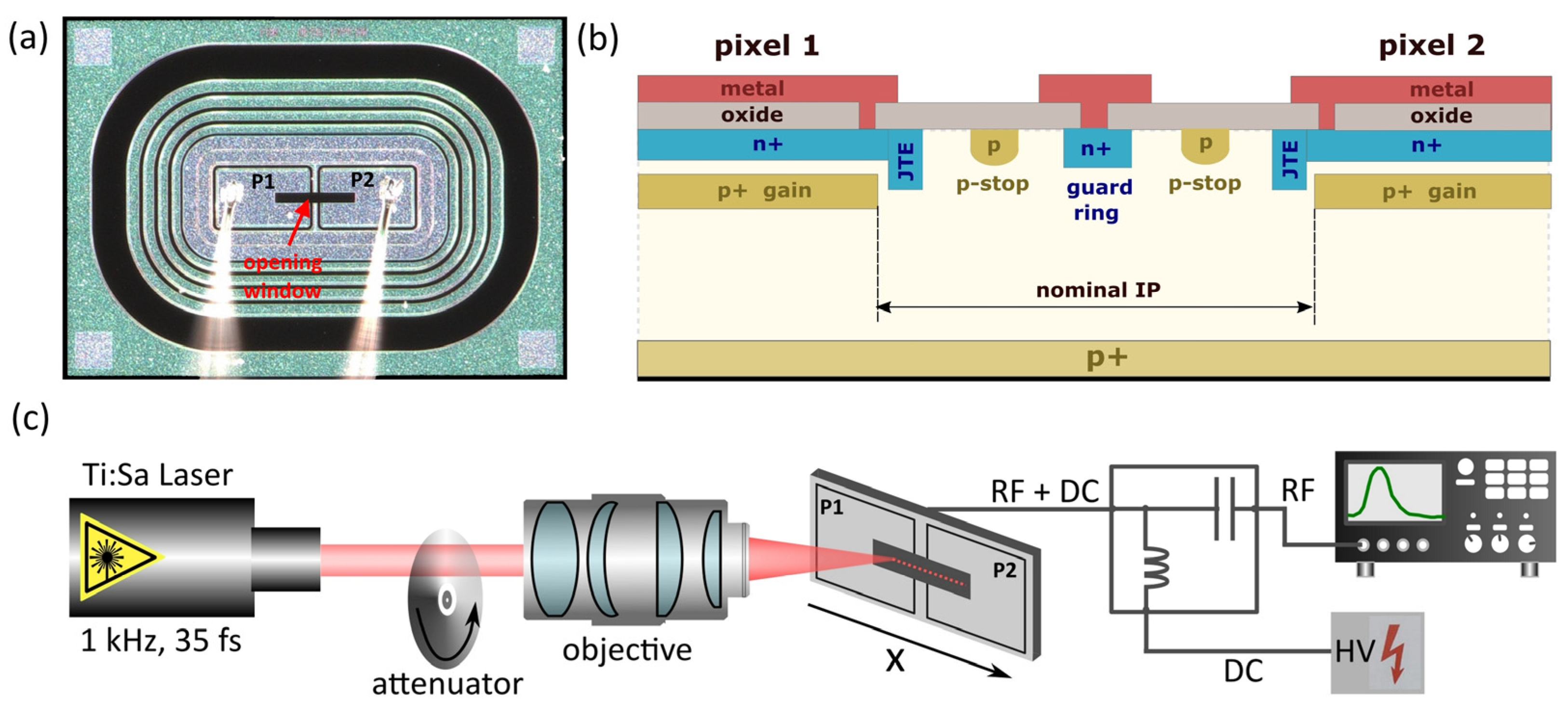
Abstract
1. Introduction
2. Materials and Methods
2.1. UFSD Productions Description
2.2. Investigated Sensor
- Layout: even if the Type 10 concept is the same (two p-stops and GR between the pixels), the nominal inter-pixel distance is 49 μm, much narrower than 61 μm in the final CMS/ATLAS layout. In addition, both the p-stops’ width and the gaps are reduced in TI-LGAD batches.
- Manufacturing process: the TI-LGAD process is not the same as the UFSD one in terms of thermal budget, materials, and other aspects. Therefore, the Type 10 samples produced on the TI-LGAD batch are not directly comparable to the standard UFSD Type 10.
2.3. Experimental Setup
3. Results and Discussion
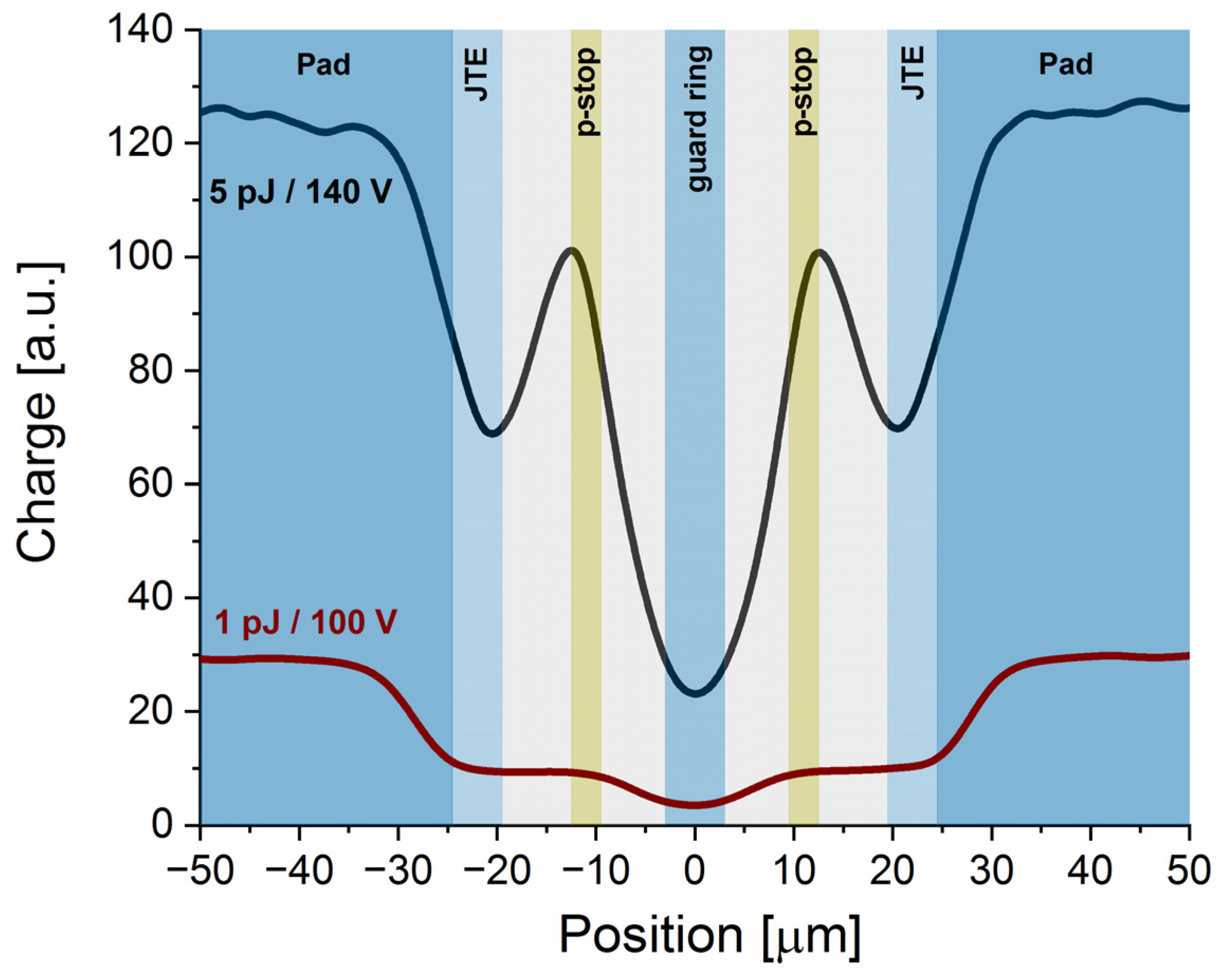
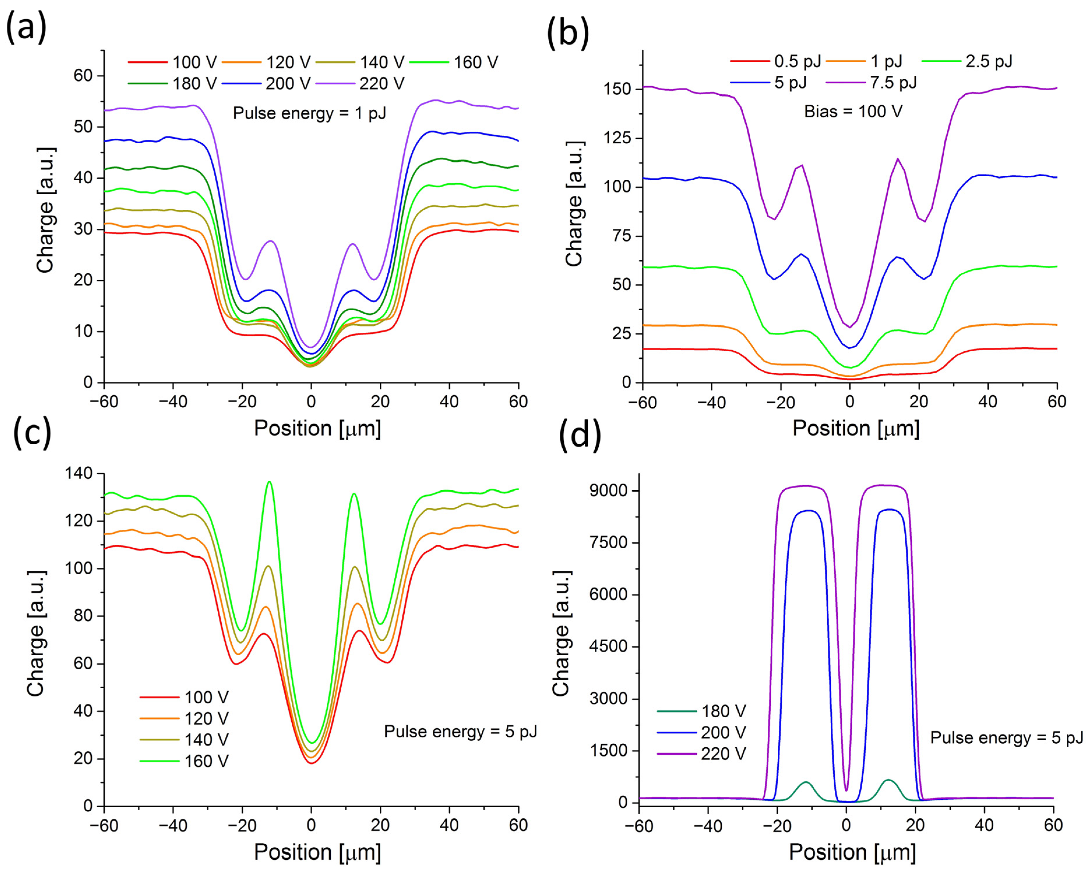
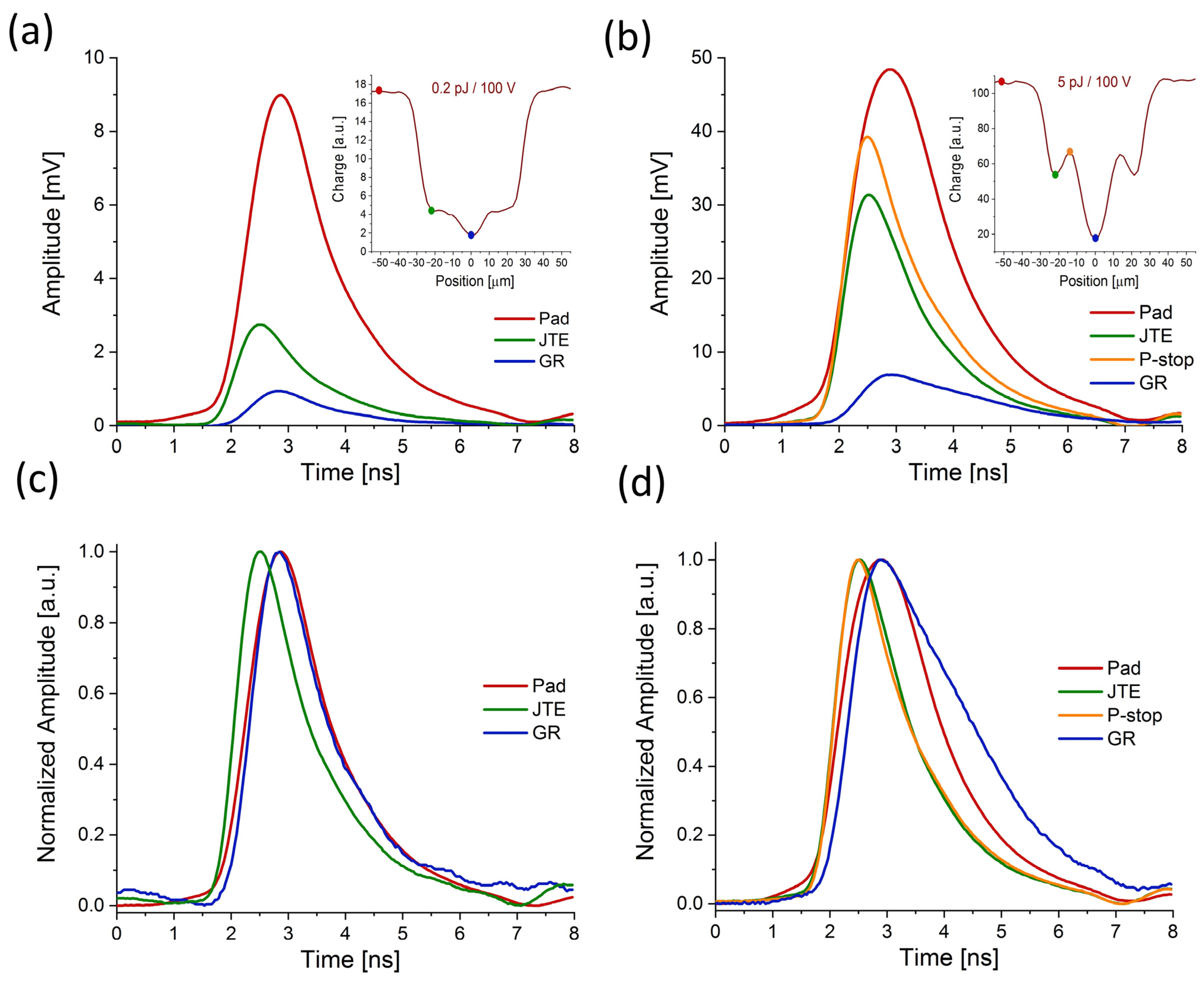
3.1. Charge Multiplication in the IP Region Observed in Charge–Spatial Profiles
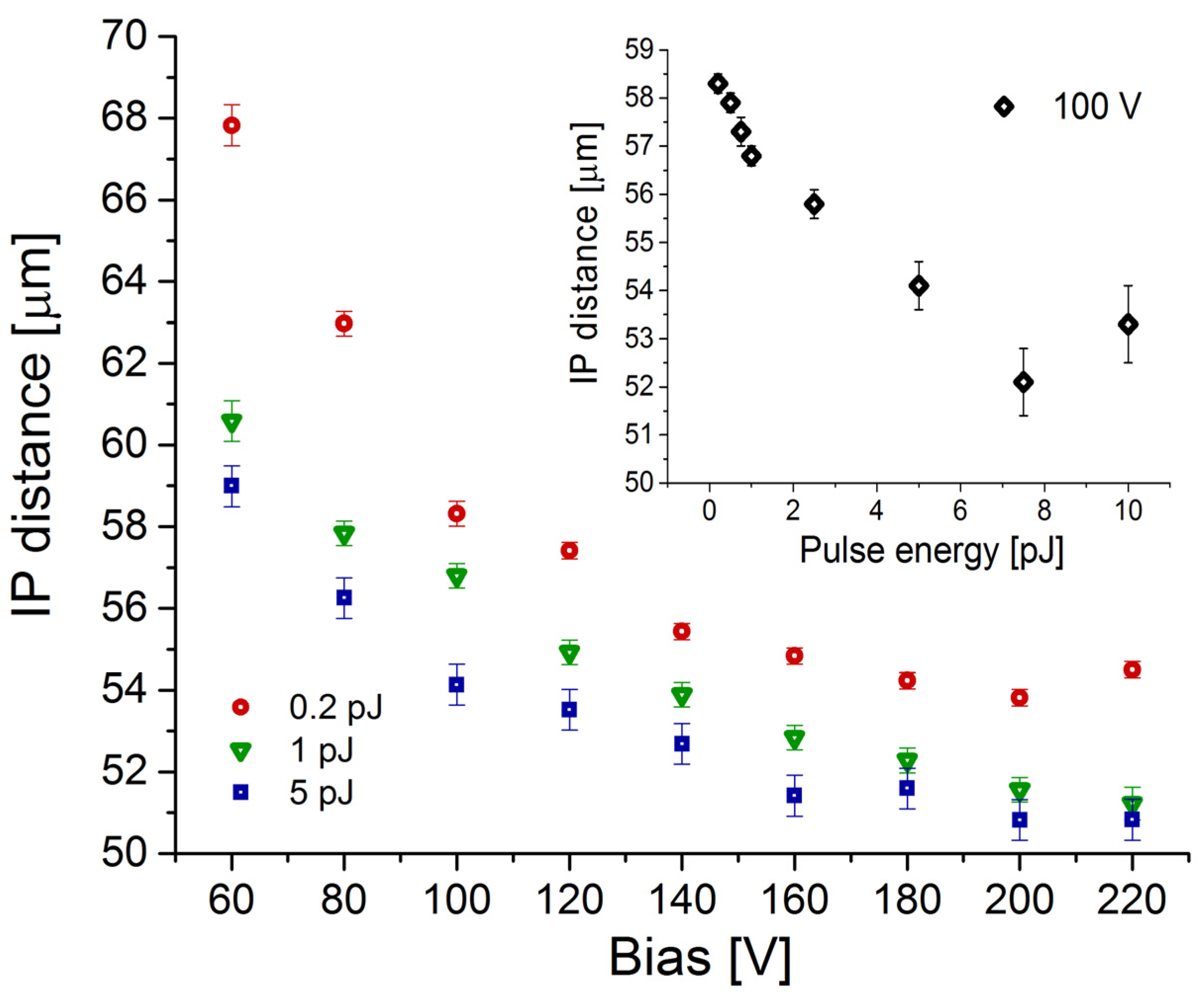
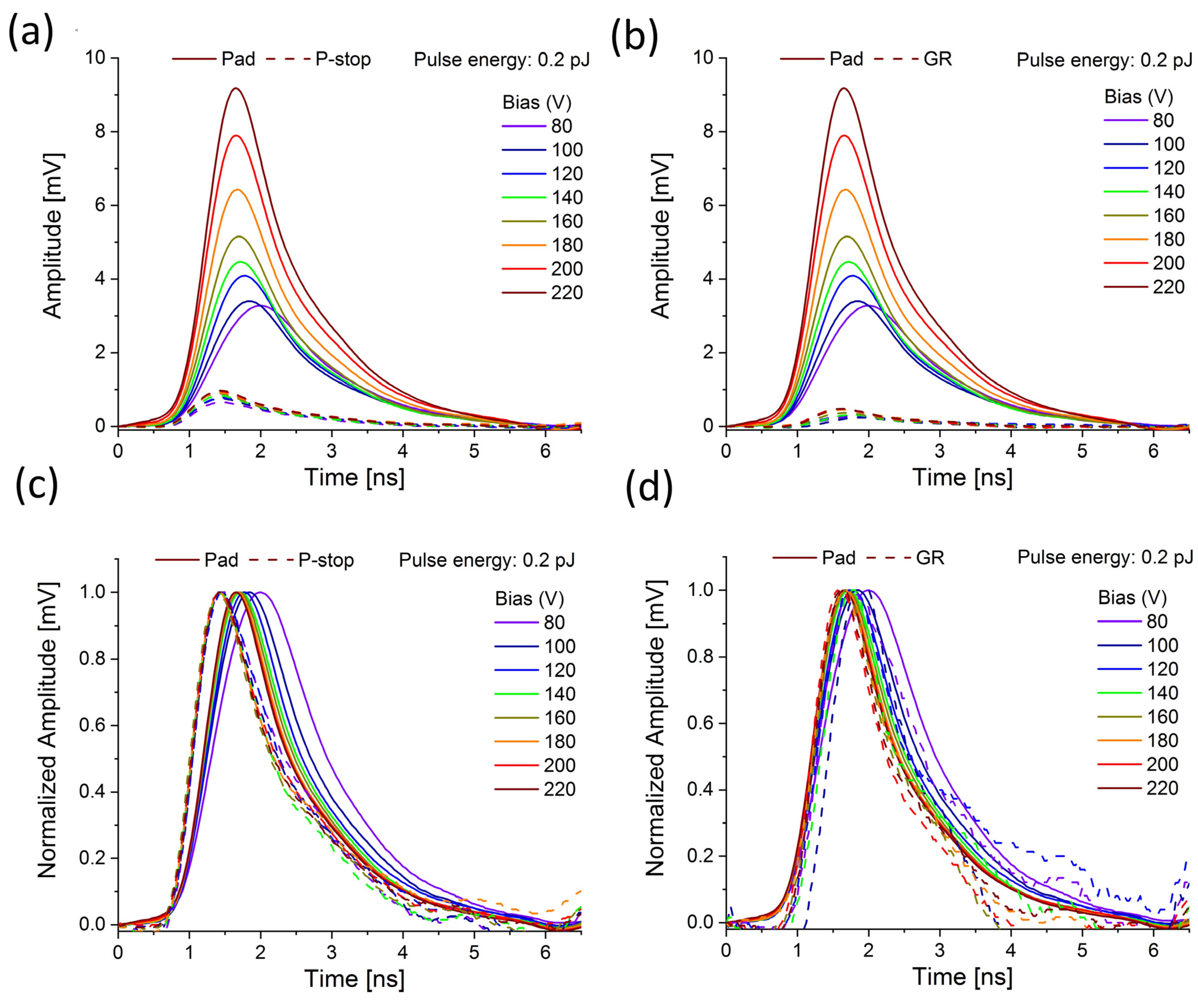
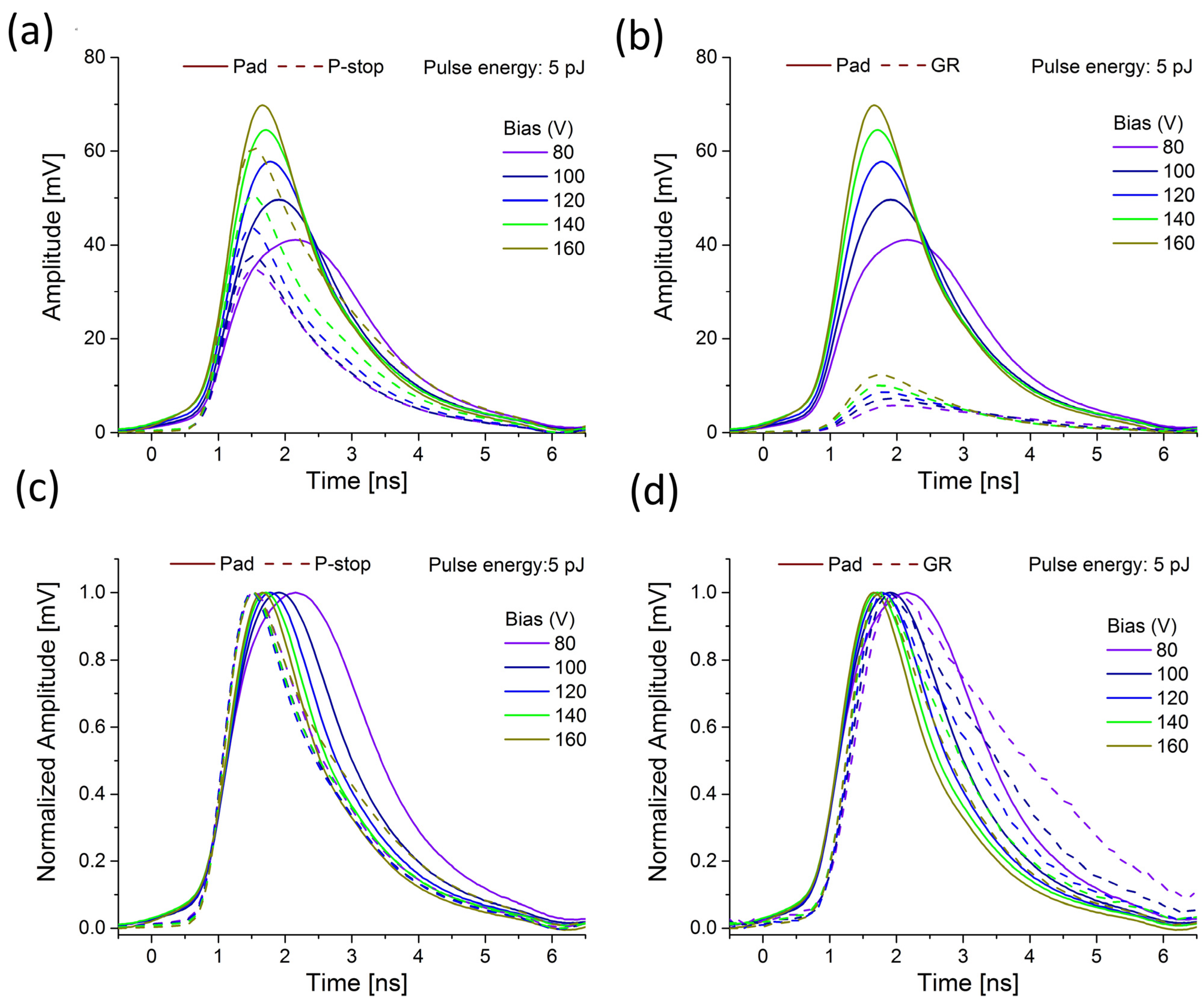
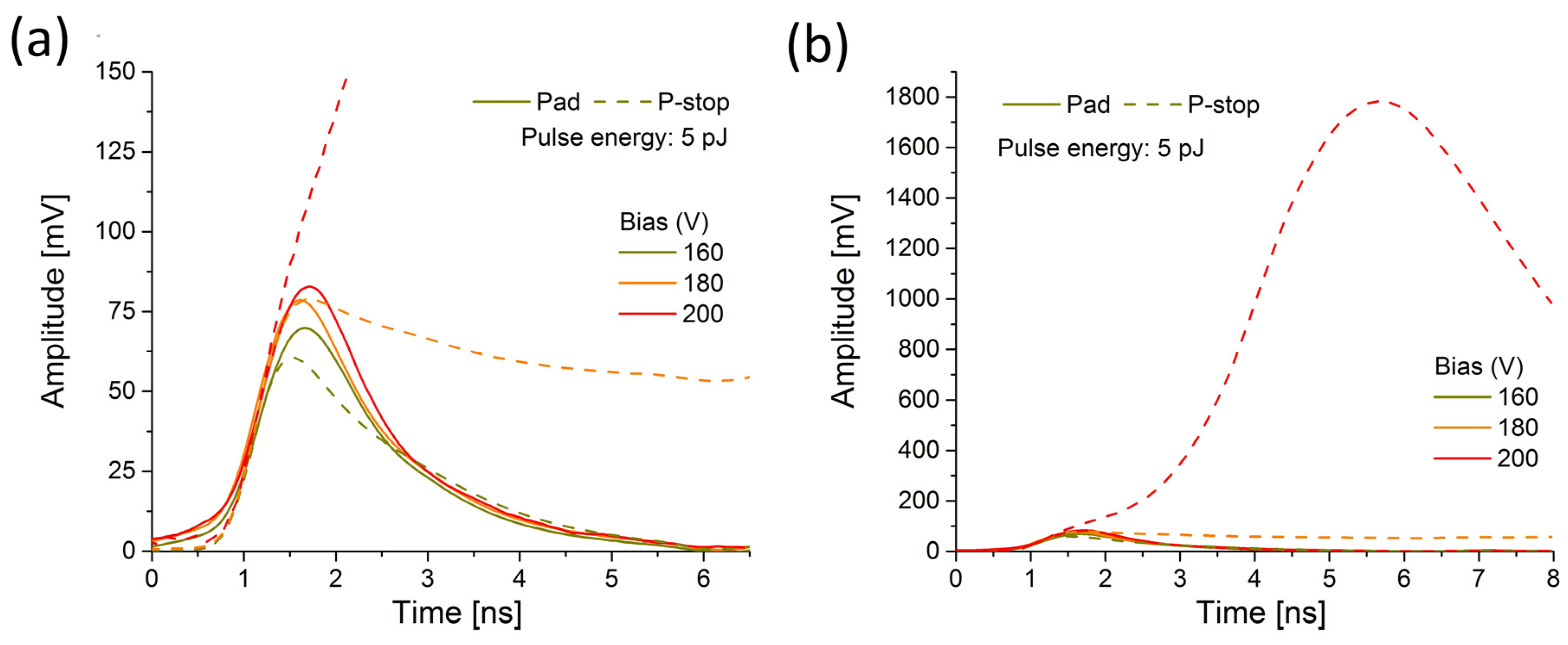
3.2. IP Distance at Different HV Bias and Pulse Energy
3.3. Evolution of Transient Current Signal Generated at Different Positions
4. Conclusions and Future Research Directions
Author Contributions
Funding
Institutional Review Board Statement
Informed Consent Statement
Data Availability Statement
Acknowledgments
Conflicts of Interest
References
- Pellegrini, G.; Fernández-Martínez, P.; Baselga, M.; Fleta, C.; Flores, D.; Greco, V.; Hidalgo, S.; Mandić, I.; Kramberger, G.; Quirion, D.; et al. Technology developments and first measurements of Low Gain Avalanche Detectors (LGAD) for high energy physics applications. Nucl. Instr. Meth. A 2014, 765, 12. [Google Scholar] [CrossRef]
- Paternoster, G.; Arcidiacono, R.; Boscardin, M.; Cartiglia, N.; Cenna, F.; Dalla Betta, G.F.; Ferrero, M.; Mulargia, R.; Obertino, M.; Pancheri, L. Development and first measurements of UltraFast Silicon Detector produced at FBK. J. Instrum. 2017, 12, C02077. [Google Scholar] [CrossRef]
- Sola, V.; Arcidiacono, R.; Boscardin, M.; Cartiglia, N.; Dalla Betta, G.F.; Ficorella, F.; Ferrero, M.; Mandurrino, M.; Pancheri, L.; Paternoster, G.; et al. First FBK production of 50 μm ultra-fast silicon detectors. Nucl. Instrum. Methods Phys. Res. Sect. A Accel. Spectrometers Detect. Assoc. Equip. 2019, 924, 360–368. [Google Scholar] [CrossRef]
- Carnesecchi, F.; Strazzi, S.; Alici, A.; Arcidiacono, R.; Borghi, G.; Boscardin, M.; Cartiglia, N.; Vignali, M.C.; Cavazza, D.; Betta, G.-F.D.; et al. Beam test results of 25 μm and 35 μm thick FBK ultra fast silicon detectors. arXiv 2022, arXiv:2208.05717. [Google Scholar]
- Sadrozinski, H.-W.; Anker, A.; Chen, J.; Fadeyev, V.; Freeman, P.; Galloway, Z.; Gruey, B.; Grabas, H.; John, C.; Liang, Z.; et al. Ultra-fast silicon detectors (UFSD). NIMA 2016, 831, 18–23. [Google Scholar] [CrossRef]
- Cartiglia, N.; Staiano, A.; Sola, V.; Arcidiacono, R.; Cirio, R.; Cenna, F.; Ferrero, M.; Monaco, V.; Mulargia, R.; Obertino, M.; et al. Beam test results of a 16ps timing system based on ultra-fast silicon detectors. NIMA 2017, 850, 83–88. [Google Scholar] [CrossRef]
- Gabriele, G. LGAD-Based Silicon Sensors for 4D Detectors. Sensor 2023, 23, 2132. [Google Scholar]
- Tornago, M. Performances of the latest FBK UFSD production. J. Phys. Conf. Ser. 2022, 2374, 012137. [Google Scholar] [CrossRef]
- Cartiglia, N.; Arcidiacono, R.; Baldassarri, B.; Boscardin, M.; Cenna, F.; Dellacasa, G.; Betta, G.-F.D.; Ferrero, M.; Fadeyev, V.; Galloway, Z.; et al. Tracking in 4 dimensions. Nucl. Instrum. Methods Phys. Res. Sect. A Accel. Spectrometers Detect. Assoc. Equip. 2017, 845, 47–51. [Google Scholar] [CrossRef]
- Ramo, S. Currents induced by electron motion. Proc. IRE 1939, 27, 584–585. [Google Scholar] [CrossRef]
- Vignati, A.; Monaco, V.; Attili, A.; Cartiglia, N.; Donetti, M.; Mazinani, M.F.; Fausti, F.; Ferrero, M.; Giordanengo, S.; Ali, O.H.; et al. Innovative thin silicon detectors for monitoring of therapeutic proton beams: Preliminary beam tests. J. Instrum. 2017, 12, C12056. [Google Scholar] [CrossRef]
- Ulrich-Pur, F.; Bergauer, T.; Burker, A.; Hirtl, A.; Irmler, C.; Kaser, S.; Pitters, F.; Rit, S. Feasibility study of a proton CT system based on 4D-tracking and residual energy determination via time-of-flight. Phys. Med. Biol. 2022, 67, 095005. [Google Scholar] [CrossRef] [PubMed]
- Andrä, M.; Zhang, J.; Bergamaschi, A.; Barten, R.; Borca, C.; Borghi, G.; Boscardin, M.; Busca, P.; Brückner, M.; Cartiglia, N.; et al. Development of low-energy X-ray detectors using LGAD sensors. J. Synchrotron Radiat. 2019, 26, 1226. [Google Scholar] [CrossRef]
- Sadrozinski, H.F.; Seiden, A.; Cartiglia, N. 4D tracking with ultra-fast silicon detectors. Rep. Prog. Phys. 2018, 81, 026101. [Google Scholar] [CrossRef]
- Paternoster, G.; Borghi, G.; Boscardin, M.; Cartiglia, N.; Ferrero, M.; Ficorella, F.; Siviero, F.; Gola, A.; Bellutti, P. Trench-Isolated low gain avalanche diodes (TI-LGADs). IEEE Electron Device Lett. 2020, 41, 884–887. [Google Scholar] [CrossRef]
- Giacomini, G.; Chen, W.; D’Amen, G.; Tricoli, A. Fabrication and performance of AC-coupled LGADs. J. Instrum. 2019, 14, P09004. [Google Scholar] [CrossRef]
- Laštovička-Medin, G.; Rebarz, M.; Kramberger, G.; Kroll, J.; Kropielnicki, K.; Laštovička, T.; Precek, M.; Andreasson, J. Femtosecond laser studies of the Single Event Effects in Low Gain Avalanche Detectors and PINs at ELI Beamlines. Nucl. Instrum. Methods Phys. Res. Sect. A Accel. Spectrometers Detect. Assoc. Equip. 2022, 1041, 167321. [Google Scholar] [CrossRef]
- Printz, M.; CMS Collaboration. P-Stop Isolation Study of Irradiated n-in-p Type Silicon Strip Sensors for Harsh Radiation Environment, Presented at 10th Hiroshima 10th International Hiroshima Symposium on the Development and Application of Semiconductor Tracking Detectors, Xian, China (Later Published as CMS CER Note No. CMS CR-2015/286). Available online: http://cds.cern.ch/record/2102890/files/CR2015_286.pdf (accessed on 10 July 2023).


Disclaimer/Publisher’s Note: The statements, opinions and data contained in all publications are solely those of the individual author(s) and contributor(s) and not of MDPI and/or the editor(s). MDPI and/or the editor(s) disclaim responsibility for any injury to people or property resulting from any ideas, methods, instructions or products referred to in the content. |
© 2023 by the authors. Licensee MDPI, Basel, Switzerland. This article is an open access article distributed under the terms and conditions of the Creative Commons Attribution (CC BY) license (https://creativecommons.org/licenses/by/4.0/).
Share and Cite
Laštovička-Medin, G.; Rebarz, M.; Doknic, J.; Bozovic, I.; Kramberger, G.; Laštovička, T.; Andreasson, J. Exploring the Interpad Gap Region in Ultra-Fast Silicon Detectors: Insights into Isolation Structure and Electric Field Effects on Charge Multiplication. Sensors 2023, 23, 6746. https://doi.org/10.3390/s23156746
Laštovička-Medin G, Rebarz M, Doknic J, Bozovic I, Kramberger G, Laštovička T, Andreasson J. Exploring the Interpad Gap Region in Ultra-Fast Silicon Detectors: Insights into Isolation Structure and Electric Field Effects on Charge Multiplication. Sensors. 2023; 23(15):6746. https://doi.org/10.3390/s23156746
Chicago/Turabian StyleLaštovička-Medin, Gordana, Mateusz Rebarz, Jovana Doknic, Ivona Bozovic, Gregor Kramberger, Tomáš Laštovička, and Jakob Andreasson. 2023. "Exploring the Interpad Gap Region in Ultra-Fast Silicon Detectors: Insights into Isolation Structure and Electric Field Effects on Charge Multiplication" Sensors 23, no. 15: 6746. https://doi.org/10.3390/s23156746
APA StyleLaštovička-Medin, G., Rebarz, M., Doknic, J., Bozovic, I., Kramberger, G., Laštovička, T., & Andreasson, J. (2023). Exploring the Interpad Gap Region in Ultra-Fast Silicon Detectors: Insights into Isolation Structure and Electric Field Effects on Charge Multiplication. Sensors, 23(15), 6746. https://doi.org/10.3390/s23156746