Article

A Compact and Efficient Boost Converter in a 28 nm CMOS with 90 mV Self-Startup and Maximum Output Voltage Tracking ZCS for Thermoelectric Energy Harvesting

Information and Communication System-on-Chip (SoC) Research Center, School of Electronics and Information, Kyung Hee University, Yongin 17104, Republic of Korea
*
Author to whom correspondence should be addressed.
Sensors 2023, 23(13), 6243; https://doi.org/10.3390/s23136243
Submission received: 6 June 2023 / Revised: 3 July 2023 / Accepted: 5 July 2023 / Published: 7 July 2023
(This article belongs to the Section Internet of Things)

Abstract

:
There are increasing demands for the Internet of Things (IoT), wearable electronics, and medical implants. Wearable devices provide various important daily applications by monitoring real-life human activities. They demand low-cost autonomous operation in a miniaturized form factor, which is challenging to realize using a rechargeable battery. One promising energy source is thermoelectric generators (TEGs), considered the only way to generate a small amount of electric power for the autonomous operation of wearable devices. In this work, we propose a compact and efficient converter system for energy harvesting from TEGs. The system consists of an 83.7% efficient boost converter and a 90 mV self-startup, sharing a single inductor. Innovated techniques are applied to adaptive maximum power point tracking (A-MPPT) and indirect zero current switching (I-ZCS) controllers for efficient operation. The startup circuit is realized using a gain-boosted tri-state buffer, which achieves 69.8% improved gain at the input VIN = 200 mV compared to the conventional approach. To extract the maximum power, we use an A-MPPT controller based on a simple capacitive divider, achieving 95.2% tracking efficiency. To address the challenge of realizing accurate voltage or current sensors, we propose an I-ZCS controller based on a new concept of maximum output voltage tracking (MOVT). The integrated circuit (IC) is fabricated using a 28 nm CMOS in a compact chip area of 0.03 mm2. The compact size, which has not been obtained with previous designs, is suitable for wearable device applications. Measured results show successful startup operation at an ultralow input, VIN = 90 mV. A peak conversion efficiency of 85.9% is achieved for the output of 1.07 mW.

1. Introduction

Recent interest in renewable energy sources is significantly increasing with rising environmental pollution and energy costs. Extensive research has been conducted to explore new methods to conserve power and harvest clean energy. Because of the increasing number of low-power devices such as the Internet of Things (IoT), wearable electronics, and medical implants, energy harvesting from renewable sources is an urgent research topic [1]. Among them, wearable devices provide important daily applications by monitoring various human activities. Diverse examples of wearable devices have been proposed, which include electronic skin, wristbands, watches, smart clothing, virtual reality (VR) headsets, and artificial intelligence (AI) hearing aids [2]. These devices demand low-cost autonomous operation with miniaturized form factors; the demands are challenging to satisfy using a rechargeable batteries. One promising energy source for wearable electronics is thermoelectric generators (TEGs), which convert an omnipresent temperature gradient into electrical energy via the Seebeck effect [3,4]. It is considered that TEGs are the only way to generate a small amount of electric power for the autonomous operation of wearable devices. Because energy conversion can be performed using a solid-state material without moving elements, TEGs are suitable for long-term operation. Under a relatively small temperature gradient, however, TEG generates a low source voltage (VS), which cannot be used to supply the devices directly. For example, commercially available TEGs generate VS between 10 mV and 30 mV for a 1 °C temperature difference [5]. Therefore, a DC-DC converter is required to boost the input to a suitable output.
Various techniques have been explored to realize efficient DC-DC converters using maximum power point tracking (MPPT) methods [6,7,8,9]. The authors of [6] configure the switching frequency based on the internal resistor (RS) of the TEG and the inductor value. However, the frequency of the on-chip clock generator can fluctuate due to process, voltage, and temperature (PVT) variations. This necessitates an adaptive MPPT controller based on a voltage-controlled oscillator (VCO) to tune the switching frequency [7]. The work conducted in [8] utilizes a hill-climbing MPPT controller that senses the output current of the converter, which charges algorithm capacitors to track VS for handling the input range from 5 μW to 10 mW. The work conducted in [9] uses transformer-based methods for a dual-stage boost converter to increase conversion efficiency to 81.5%.
The switched capacitor (SC)-based approach offers the advantage of on-chip integration and low-voltage operation [10,11,12]. The gate-boosted charge pump operates with an input voltage of 100 mV [10]. Another work [11] utilized a voltage doubler as a negative charge pump to reduce the on-resistance of the load-side switch. Additionally, a fully integrated SC converter used a 220 mV input to generate a 1.9 V output [12]. However, previous works have the drawback of large system sizes; for example, the algorithm capacitor in [8] requires a 7.6 mm2 silicon area. Other works have bulky implementations, such as a transformer of 1.8 mm2 size [9], a sizeable on-chip capacitor of 2.31 mm2 [10], and three inductors [13]. The SC-based converter shows relatively low efficiencies, for example, 33% [10], 52% [11], and 37.4% [12].
Because VS can be smaller than the threshold voltage (VTH) of transistors, a self-startup method is required for the initial step-up of the supply voltage. The startup temporarily provides power for the main converter until it can be self-sustained. Various methods have been investigated. These methods include using a mechanical switch to initiate the converter [6], utilizing an off-chip transformer [9], using on-chip inductors [10], and pre-charging the output capacitor using an external battery [14]. However, these techniques often demand bulky implementations, which can be impractical for low-cost sensor nodes and IoT applications. The works [15,16] use the switched branches for inductor sharing between the startup and main converter; however, the switching increases the system complexity.
The discontinuous conduction mode (DCM), commonly used for low-power DC-DC converters, should suppress the reverse current through the inductor. The high-side switch is opened when the inductor current IIND is close to zero for zero current switching (ZCS). One method to implement ZCS is using a diode [17]; however, this approach is unsuitable for low-voltage design due to diode voltage drop. For efficiency reasons, a transistor switch is typically used with a ZCS controller. A previous work on a ZCS controller used a comparator to detect the voltage [18]. Another approach is to use digital circuits to detect current zero crossing indirectly using the inductor voltage [19]. The digital quantization of inductor voltage needs to select fine pulse width for the ZCS operation. However, the linear scaling used to modulate the pulse width becomes inefficient for low VIN. To handle the issue, a fine delay stage is used [20], which sets the pulse width suitable to open the high-side switch; however, the ZCS controller uses an external supply to realize fine delay. In addition, appropriate measurement delay is not addressed [21].
To overcome the issues mentioned above, we propose a compact and efficient DC-DC converter system realized in the 28 nm CMOS technology. The integrated system consists of an 85.9% efficient boost converter and a 90 mV self-startup, sharing a single inductor. Innovated techniques are applied to adaptive MPPT (A-MPPT) and indirect ZCS (I-ZCS) controllers for efficient operation. The startup circuit is realized using a ring-oscillator-based charge pump, which enhances gain using a tri-state buffer for ultralow voltage operation. The tri-state buffer achieves a 69.8% gain improvement over a single buffer at VIN = 200 mV. To extract the maximum power, we use an A-MPPT controller based on a simple capacitive divider for fractional open circuit voltage (FOCV) operation. To address the challenges of realizing accurate voltage or current sensors, we propose an I-ZCS controller based on maximum output voltage tracking (MOVT). The fabricated integrated circuit (IC) is realized in a compact chip area of 0.03 mm2. The compact size, which has not been obtained with previous designs, is suitable for wearable device applications. The measured results show a peak tracking efficiency of 95.2% and a conversion efficiency of 85.9%. The end-to-end efficiency of 83.7% is achieved using RS = 8 Ω and VS = 280 mV.
This paper is organized as follows. Section 2 describes the system design. Section 3 presents the circuit implementation. Section 4 presents the measured results, and Section 5 draws the conclusion.

2. System Design

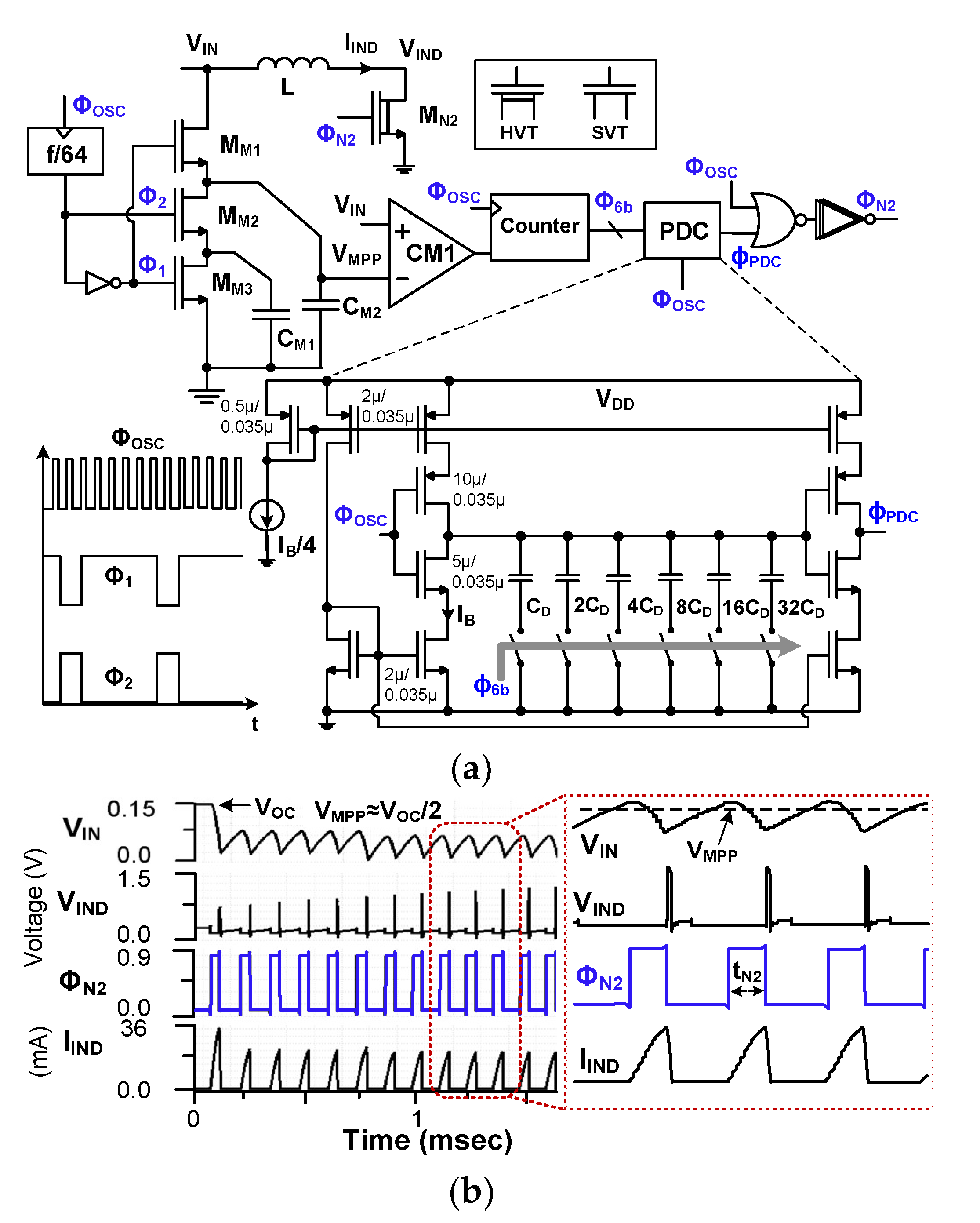
2.1. Proposed System

Figure 1 shows the block diagram of the proposed system. It mainly consists of a boost converter and a self-startup circuit. The boost converter includes an A-MPPT controller, an I-ZCS controller, a voltage detector (VD), an oscillator, and four power switches (MN1, MN2, MP1, and MP2). MN1, used for self-startup, is a low threshold voltage (LVT) transistor. High threshold voltage (HVT) transistors are used for the switches of the boost converter (MN2, MP1, and MP2), which reduces the leakage current compared to the standard threshold voltage (SVT) transistor. Super-low threshold voltage (SLVT) transistors are used for the startup circuit to reduce the minimum input VIN to the system. The oscillator consists of a ramp generator, pulse generator, biasing resistor ROSC, and capacitor COSC. The ramp voltage VRAMP is compared with a reference VREF to generate the clock signal ΦOSC for the A-MPPT controller. The TEG is modeled using VS and RS. An input capacitor CIN is used to buffer the converter’s input VIN. A single inductor L = 100 μH is shared between the startup and boost converter without extra switches.
Figure 2 shows the waveform of the converter. When VIN is supplied to the startup circuit, it generates an output pulse ΦS,OUT (=ΦN1) for MN1. During the on-time of MN1, L is charged when VIN is as low as 90 mV. During the off-time of MN1, stored energy in L keeps charging the storage capacitor CDD through MP1. During the startup, the supply voltage VDD gradually increases to 700 mV. The VD monitors VDD. When VDD reaches 700 mV, it generates the disable signal VDIS, which stops the oscillation of the startup circuit and enables the boost converter. The boost converter raises the tens of mV generated by the TEG to the output VOUT level required to power IoT devices. To extract the maximum power from the TEG, the A-MPPT controller continuously adjusts the on-time of the pulse ΦN2 for MN2. Then, the input impedance RIN is adjusted to match RS, and the maximum power point (MPP) voltage VMPP tracks half of VS. The I-ZCS controller provides the pulse ΦP2 to control the on-time of MP2 when L discharges. The MP2 is turned off at a suitable time to prevent the current backflow from VOUT.

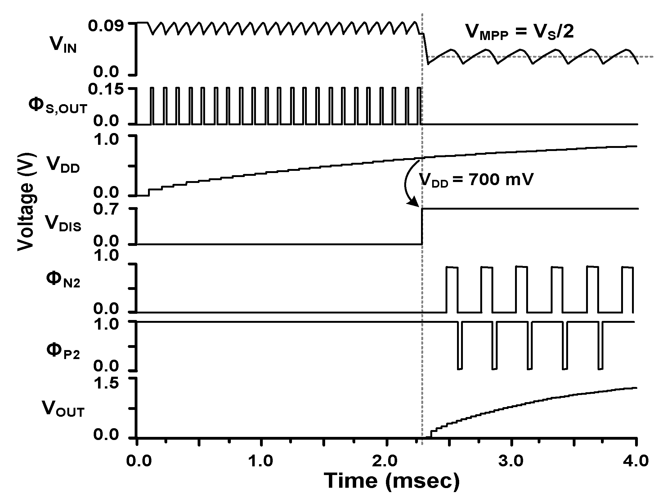
2.2. Self-Startup Circuit

Ring oscillators are widely used to generate the clock for the startup circuit; however, the operation is limited mainly by two reasons. Firstly, when VDD reduces, it is difficult to sustain the oscillation with the decreased gain of the inverter. Secondly, the output swing needed to drive the subsequent stage is reduced. These limitations can significantly impede the low-voltage startup [22].
Figure 3 shows the proposed self-startup circuit using a gain-boosted tri-state buffer. It consists of six stages, in which the output of the fifth stage is feedback to the first stage. The inset shows the schematic of the unit stage. It comprises two inverters, INV1 (transistors N1 and P1) and INV2 (transistors N2 and P2). They are realized using SLVT transistors to reduce the startup voltage further. The INV2 works as a tri-state buffer, which provides additional gain to reduce the input for the startup. VEN is enabled by the input, and the startup circuit generates ΦS,OUT. When disabled, it keeps a high impedance state. The voltage gain AV1 of a single inverter can be expressed [22] as
A V 1 g m , eff 1 g ds , N 1 + g ds , P 1 = g m , N 1   + g m , P 1   g ds , N 1 + g ds , P 1
where the effective transconductance gm,eff1 is the transconductance sum of N1 and P1. The gds,N1 and gds,P1 are the output conductance of N1 and P1, respectively. In the proposed gain-boosted buffer, the input VBuf,in is fed to the gate of the two inverters. The buffer output VBuf,out is taken from the output of INV2. The output of INV1 is connected to the source of the P2, which is amplified by the gain (AV1VIN) of INV1. Then, it is increased to (1 + AV1)VIN. Because AV1 > 1, VBuf,in is amplified by the effective transconductance gm,eff2 of the tri-state buffer, which can be written as
g m , eff 2 ( 1 + A V 1 ) g m , P 2 + g m , N 2
where gm,P2, and gm,N2 are the transconductance of P2 and N2, respectively. Using a similar method to that used to derive Equation (1), we obtain the gain AV2 of the gain-boosted buffer as
A V 2 g m , eff 2   g ds , P 2 + g ds , N 2 = ( 1 + A V 1 ) g m , P 2   + g m , N 2   g ds , P 2 + g ds , N 2
where gds,N2, and gds,P2 are the output conductance of N2 and P2, respectively. The result shows an enhanced gain of the tri-state buffer.
Figure 4a shows the transfer characteristics of the single- and tri-state buffers for three VIN. The tri-state buffer shows steeper slopes, indicating increased gain. The gain is calculated by taking the derivative of VBuf,out. Figure 4b shows the gain comparison using VIN = 100 mV. The result indicates that the tri-state buffer achieves a 21.2% gain improvement. Figure 4c,d show the gain comparison using VIN = 150 mV and VIN = 200 mV, respectively. The results show that the tri-state buffer increases the gain by 41.1% and 69.8%, making it an attractive approach for low-voltage startups.

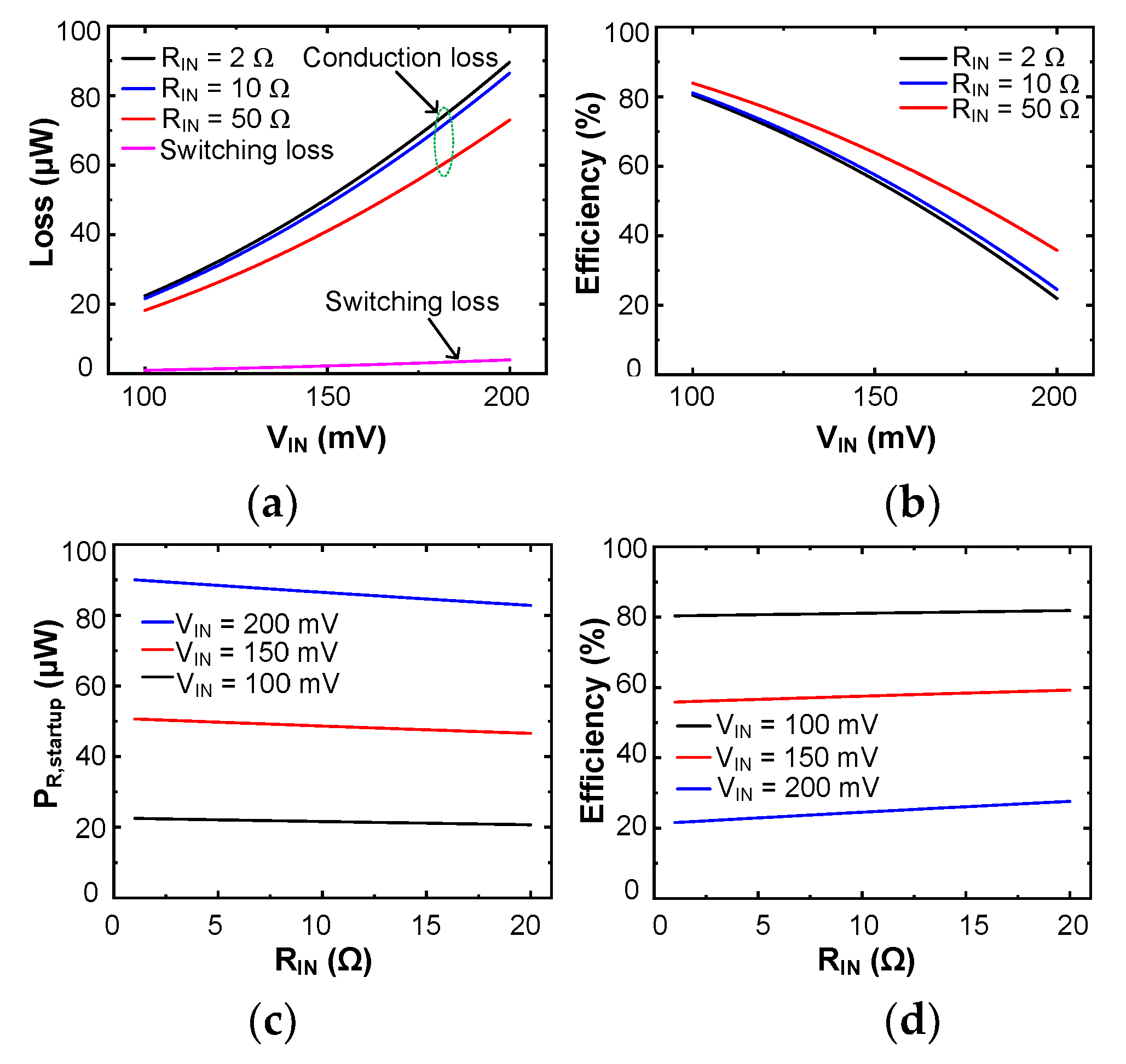
2.3. Loss Analysis for Startup

Figure 5 shows the equivalent circuit of the startup for loss analysis. The resistive power loss PR,startup of the startup circuit can be expressed as
P R , startup R 0 V IN 2 ( R IN + R 0 ) 2 = ( R IND + R N 1 ) V IN 2 ( R IN + R IND + R N 1 ) 2
where R0 consists of the inductor parasitic resistance RIND (= 120 mΩ) and the resistance RN1 of MN1. The switching loss PSW,startup can be expressed as
P SW , startup 1 2 C G , N 1 V G , N 1 2 f St
where fSt is the switching frequency of the startup circuit. VG,N1 and CG,N1 are the gate voltage and capacitance of MN1, respectively. The power consumption PQ,startup of the startup circuit is 60 nW using VS = 150 mV and RS = 18 Ω. The total loss PT,startup is the sum of PR,startup, PSW,startup, and PQ,startup. Using the input power PIN, we obtain the efficiency ηstartup of the startup circuit as
η startup = P IN P T , startup P IN
Figure 6a shows the calculated loss of the startup circuit as a function of VIN. PR,startup increases with VIN, and PSW,startup is negligible compared to PR,startup with a relatively low fSt ≈ 40 kHz. Figure 6b shows that ηstartup decreases when VIN increases for a given RIN. Figure 6c shows that PR,startup decreases slightly with RIN, which is mainly determined by VIN. Figure 6d shows that ηstartup increases with RIN while decreasing with VIN, which is attributed to increased PR,startup. In summary, increasing VIN leads to elevated PR,startup and reduced ηstartup. Increasing RIN results in reduced PR,startup and improved ηstartup.

2.4. Loss Analysis for Boost Converter

Figure 7 shows the equivalent circuit of the converter for loss analysis. The resistive power loss PR,boost of the boost converter can be written as
P R , boost = I CHA ¯ 2 ( R IND + R N 2 ) + I DIS ¯ 2 ( R IND + R P 2 )
where I C H A ¯ is the average inductor charging current when MN2 is on, and I D I S ¯ is the average discharging current when MP2 is on (MN2 is off). RN2 and RP2 are the on-resistances of MN2 and MP2, respectively. In the typical boost converter, we can neglect the loss of MP2 with the condition of ( I C H A ¯ I D I S ¯ ). The switching loss PSW,boost can be expressed as
P SW , boost = 1 2 ( C G , N 2 + C PAR ) V DD 2 + C G , P 2 ( V OUT V TH , P 2 ) 2 f S 1 2 C G , N 2 + C G , P 2 + C PAR V DD 2 f S
where fS is the switching frequency, and we use the approximated relationship of VDD ≈ (VOUTVTH,P2). Here, VTH,P2 = 0.52 V is the threshold voltage of MP2. CG,N2 and CG,P2 are the gate capacitance of MN2 and MP2, respectively. CPAR = 21 pF is the parasitic capacitance. We obtain PSW,boost = 200 nW using fS = 8 kHz, and VDD = 0.9 V. The quiescent power PQ,boost of the boost converter is 420 nW. The total power loss PT,boost of the boost converter is the sum of PR,boost, PSW,boost, and PQ,boost. The synchronization and leakage losses are neglected to simplify the analysis. Then, we obtain the end-to-end efficiency ηEE of the boost converter as
η EE = P OUT P Max = P Max P T , boost P Max
where PMax = (VS)2/(4RS) is the maximum available power from the source, and POUT = (VOUT)2/RL is the output power with the load resistance RL.
Figure 8 shows the calculated ηEE as a function of RS for different VS using the switch parameters shown in Table 1. When RS is reduced, increased I C H A ¯ and PR,boost reduces ηEE. The ηEE improves with increasing RS for a given VS. For RS = 8 Ω and VS = 300 mV, ηEE increases to 89.3%. Beyond the maximum point, increasing RS reduces ηEE by the decreased PMax.

3. Implementation

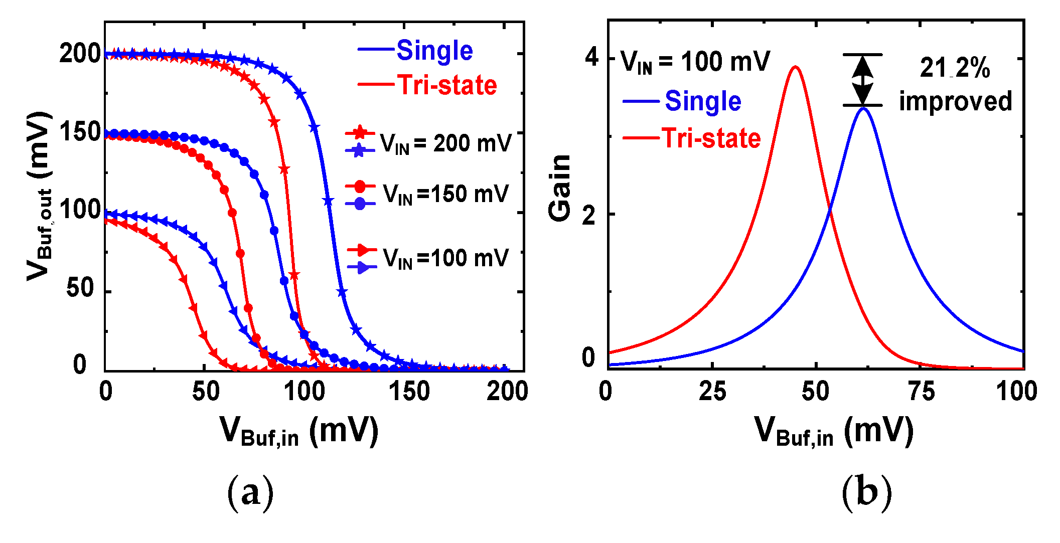
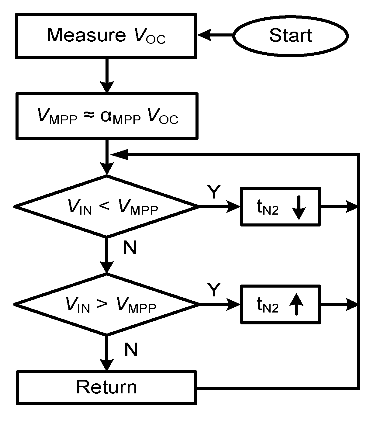
3.1. Adaptive MPPT Controller

Figure 9a shows the schematic of the A-MPPT controller. It consists of a capacitor-based FOCV sampler, a comparator CM1, a counter, a programmable delay controller (PDC), and logic gates. In the FOCV technique, VMPP ≈ (αMPPVOC) is obtained using the sampled open-circuit voltage VOC (≈VS) and a source-dependent coefficient αMPP, where αMPP = 0.5 is used for the TEG. The capacitive divider (CM1 and CM2) generates VMPP. When Φ1 is high (Φ2 is low), switch MM1 is turned on, and VOC is stored in CM2. When Φ2 is high (Φ1 is low), switch MM2 is turned on. The stored charge in CM2 is shared with CM1. Then, the voltage VMPP across CM2 becomes half of VOC. CM1 compares VIN against VMPP, which decides the direction of the up/down counter. The counter output sets the delay of the PDC, and the on-time tN2 of ΦN2 is adjusted by the capacitor array in the PDC.
The RIN of the DCM operation can be expressed [9] as
R IN = 2 L t N 2 2 f S
where we vary tN2 to adjust RIN while keeping fS constant. To facilitate the MPPT operation, the oscillator frequency fOSC, which is higher than fS, is used to update tN2. This method is different from a previous approach [23], which adjusts tN2 after evaluating VMPP rather than choosing between different VMPP values. Figure 9b shows the simulated waveforms of the MPPT operation. In the beginning, VIN increases to VOC by the sampling operation. Using the output of CM1, the A-MPPT controller adjusts tN2 to vary RIN for tracking the VIN changes occurring between two consecutive VMPP values. The A-MPPT controller consumes 430 nW at VDD = 900 mV.
Figure 10 shows the flowchart further explaining the MPPT operation. The operation is based on the approximately linear relationship between VOC and VMPP. By leveraging this relationship, tN2 is adjusted to control RIN and VIN. In the case of (VIN < VMPP), tN2 is decreased to increase RIN and VIN. Conversely, tN2 increases to reduce RIN. The proposed approach is simple since it requires measurements of only VOC, even during temperature variations. Figure 11 shows the schematic of CM1. It is based on a PMOS differential input pair and is biased, using IBIAS = 5 nA. The power consumption of CM1 is 40 nW at VDD = 0.9 V.

3.2. Indirect ZCS Controller
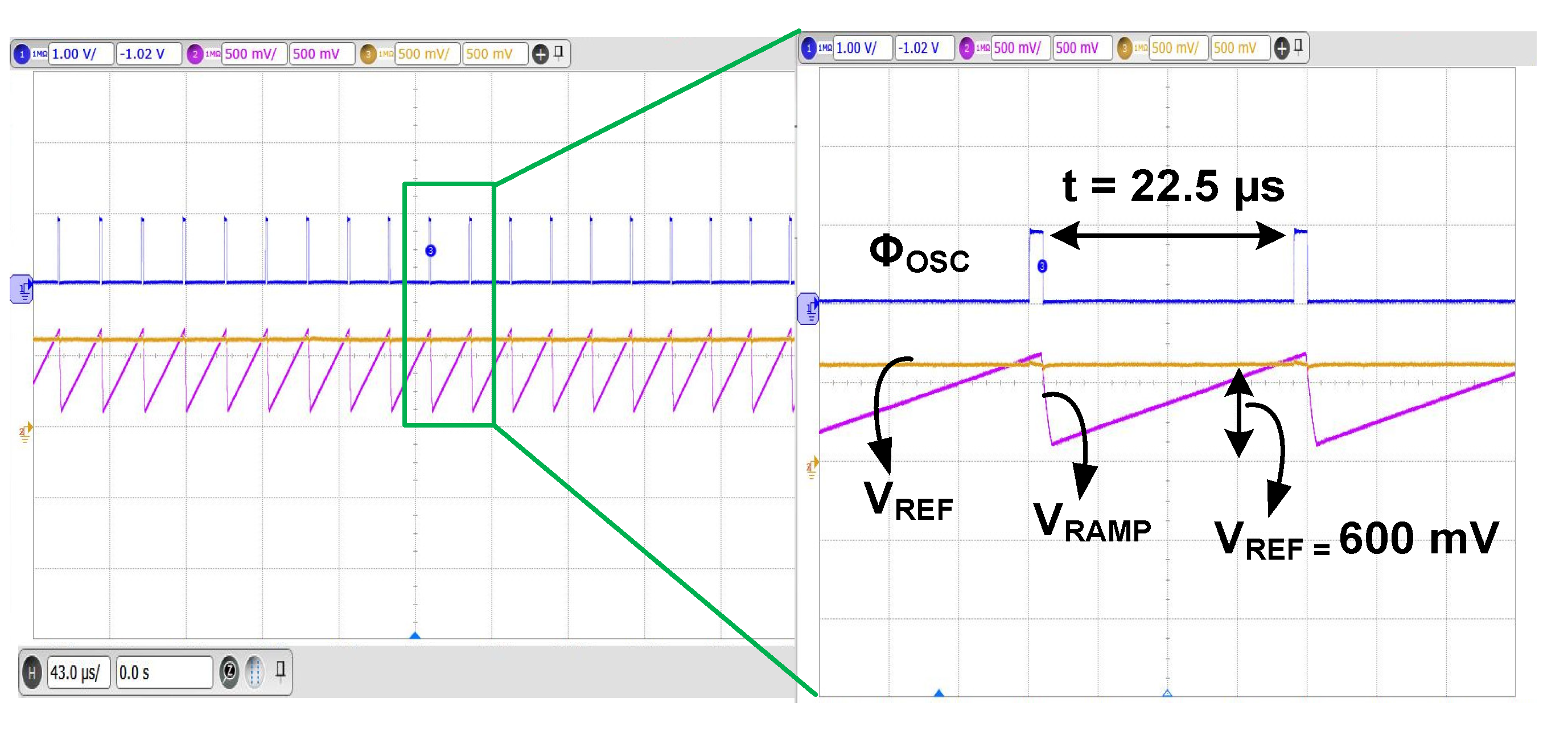
Figure 12a shows the schematic of the I-ZCS controller. It comprises a comparator CM2, a counter, a PDC, sampling capacitors (C1,2,3), and logic gates. The CM2 compares the current average output VOUT,AVG(n) against the previous output VOUT,AVG(n−1), which is obtained via the low pass filter (RZ, CZ). The CM2 outputs the up/down signal ΦU/D for the counter, followed by the PDC that generates the adjustable delay ΦP2 for MP2. Using the 6-b output Φ6b, PDC either increases or decreases the on-time tP2 of ΦP2. The PDC used for the I-ZCS controller has a similar structure to the one used in the A-MPPT controller. The ΦN2 is input to the PDC to set the starting reference for ΦP2 since the on-time of ΦN2 is used for inductor charging, while the on-time of ΦP2 is used for inductor discharging. At the end of discharging, the ZCS operation is performed.
Using the waveform of IIND, we can derive the expression for the change ΔtP in terms of output change ΔVOUT = [VOUT,AVG(n) − VOUT,AVG(n−1)] as
Δ t P 2 L t N 2 R OUT f S Δ V OUT V OUT
where ΔtP2 is the difference between the current tP2(n) and the previous tP2(n − 1). The derivation of the above relation is shown in Appendix A. The nomenclature used for the acronyms and symbols of this paper are listed in Appendix B. The working principle of the I-ZCS controller is based on MOVT. VOUT is maximized when optimal tP2 is set for ZCS. In either case, when IIND falls to zero before or after MP2 is switched off, the non-optimal ZCS operation reduces VOUT; when there is perfect inductor zero crossing, VOUT is maximized. One advantage of an I-ZCS operation is that no IIND sensor is needed. The tN2 of ΦN2 is determined by the A-MPPT controller, depending on the source impedance RS. The tN2 does not have a direct effect on the I-ZCS controller since it is independently determined before the ZCS operation.
Waveforms for explaining I-ZCS operation are also shown. When VOUT,AVG(n) is greater than VOUT,AVG(n−1), the positive difference (ΔVOUT > 0) performs down-counting with low ΦU/D. The PDC reduces the number of active delay capacitance, decreasing the pulse width of tP2. Conversely, the opposite condition (ΔVOUT < 0) performs up-counting to increase tP2. Then, ΦU/D switches between high and low until it reaches the steady state, when VOUT is maximized by optimal ZCS operation. One drawback of this approach is that VOUT is not fully regulated, which can be handled using additional regulators commonly used for various power supplies.
Figure 12b shows the logic operation to generate VOUT,AVG(n − 1). After ΦN2 is turned off, ΦP2 turns on MP2. The output ΦQ is kept high until ΦP2 becomes high. With a high transition of ΦP2, the output ΦQ of the J/K flip-flop becomes low. When ΦP2 becomes low, ΦNOR becomes high, which allows C2 to be charged from C1. When ΦNOR changes to low due to the rising ΦP2, the voltage VC2 across C2 is transferred to C3, generating VOUT,AVG(n − 1). Figure 13 shows the simulated results of the I-ZCS controller. During the on-time of ΦN2, IIND increases. When ΦN2 turns off and ΦP2 turns on, IIND decreases. The result shows that ΦP2 accurately switches off when the zero crossing of IIND occurs. When IIND reaches zero, MP2 turns off, initiating the DCM period indicated by TDCM. The result shows the successful operation of the proposed I-ZCS controller.

4. Measured Results

Figure 14a shows the micrograph of the converter IC fabricated using a 28 nm CMOS process in an area of 0.03 mm2. The IC is mounted on a test board using the chip-on-board (COB) technique. Figure 14b shows the experimental setup for the converter characterization. A digital meter (DMM6500) is used for measuring the current. The DC power supply emulates the TEG source from 0.1 V to 0.4 V. The commercial TEG source is also used for testing [24].
Figure 15 shows the measured waveform of the oscillator. When VRAMP is higher than VREF = 600 mV, ΦOSC is triggered high. The measured frequency of ΦOSC is 44.4 kHz. Figure 16a shows the measured transient result of the self-startup. Using VIN = 250 mV and RS = 20 Ω, VDD is increased to 700 mV, which is enough to enable the boost converter. The steady state is reached after 2 sec. Using the commercial TEG having VIN = 200 mV, VDD is increased to 600 mV, and the steady state is reached after 5 sec. These results demonstrate the successful operation of the self-startup. We further characterize the startup circuit using reduced VIN. Figure 16b shows the measured result, in which VIN = 90 mV is increased to VDD = 650 mV. The result shows that the gain-boosted tri-state buffer effectively reduces the minimum startup voltage.
Figure 17 shows the measured waveforms of the converter. The experiment is performed using VIN = 250 mV and RS = 20 Ω. When ΦN2 is high, L is charged. When ΦN2 is triggered to low, the energy stored in L is transferred to the output. When VIND reaches the ground, ΦP2 becomes high to turn off MP2 via the I-ZCS controller. The ringing is caused by the LC resonance when MP2 is turned off. Overall capacitance, including CL, forms resonance with L, and the amplitude is decayed by the path loss.
Figure 18a shows the measured tracking efficiency ηMPPT = (PIN/PMax) as a function of VS. The results show that ηMPPT > 93% is achieved in the VS range from 135 mV to 300 mV, with the peak ηMPPT of 95.2%. Figure 18b shows the measured conversion efficiency ηCONV = (POUT/PIN) as a function of POUT. POUT is changed from 77 μW to 1.28 mW by varying RL. The peak ηCONV = 85.9% is achieved for POUT = 1.07 mW. Figure 19 shows the measured ηEE = (POUT/PMax) of the converter as a function of VS for different RS. Because PMax is reduced, ηEE decreases with increasing RS. The result shows that peak ηEE = 83.7% is achieved using RS = 8 Ω and VS = 280 mV.
Table 2 shows the comparison with previous works using the boost converter for energy harvesting [25,26,27,28,29,30,31,32]. Our approach introduces a novel technique for self-startup using the tri-state buffer, distinguishing it from the studies conducted in [26,29], which relied on a single buffer. Notably, the proposed self-startup circuit achieves a minimum startup voltage of 90 mV, outperforming all the works except [30]. Furthermore, our proposed A-MPPT and I-ZCS controllers achieve a relatively high conversion efficiency of 85.9%. In comparison, the efficiencies observed in [25,28,32] are 74.5%, 75.0%, and 25.0%, respectively. In addition, our compact design has the smallest chip area (0.03 mm2) among the works, including ICs implemented using the same technology node of a 28 nm CMOS [31,32]. The result shows that our work effectively handles the previous issue of bulky implementations. Consequently, our research provides practical and efficient solutions for low-cost wearable electronics and IoT applications.

5. Conclusions

In this paper, we propose a compact and efficient boost converter in a 28 nm CMOS for thermoelectric energy harvesting. For self-startup, we use a gain-boosted tri-state buffer in a ring oscillator to achieve a 90 mV minimum startup. A comparison with the single inverter shows that the proposed tri-state buffer achieves a 69.8% improvement in the DC gain. To extract the maximum power from the TEG, we use a FOCV-based A-MPPT controller. To remove the current sensor required by the conventional approach, we propose an I-ZCS controller to achieve an efficient DCM operation. The converter is fabricated in a 28 nm COMS process realized in a compact area of 0.03 mm2. The measured data show a successful I-ZCS operation using the proposed MOVT technique. Using the A-MPPT controller, the converter achieves a peak tracking efficiency of 95.2%. The converter delivers the output power of 1.07 mW with a peak conversion efficiency of 85.9%. Using the proposed techniques, TEG energy harvesting can be realized in a compact system. These characteristics are suitable for various applications, including wearable electronics, medical implants, and IoT devices.

Author Contributions

M.A. designed the circuit, performed the experimental work, and wrote the manuscript. S.C.C. supported measurement. S.-Y.M. supported design kit setup and measurement. M.S.J., A.S. and H.Q. edited the manuscript. J.-W.L. conceived the project, organized the paper content, and edited the manuscript. All authors have read and agreed to the published version of the manuscript.

Funding

This work was supported in part by the Basic Science Research Program from the National Research Foundation of Korea (No. 2021R1A2B5B01001475) and in part by the National R&D Program from the National Research Foundation of Korea, funded by the Ministry of Science and ICT (No. 2020M3H2A1076786).

Acknowledgments

The chip fabrication and CAD tools were supported by the IDEC (IC Design Education Center).

Conflicts of Interest

The authors declare no conflict of interest.

Appendix A

Figure A1 shows the inductor current IIND waveform of the boost converter. The IIND is the sum of ICHA during tN2 and IDIS during tP2. Assuming VIN slowly varies during the conversion, the voltage difference across L for ICHA can be expressed as
V IN 0 = L d I IND d t L I P t N 2
where IPVIN(tN2/L) denotes the peak current. Using the voltage across the inductor at tP2, we obtain another expression for the peak current IP:
I P = ( V OUT V IN ) t P 2 L
Figure A1. Inductor current waveform of the boost converter.
Sensors 23 06243 g0a1
The average current is obtained by integrating the current within the switching cycle and is equivalent to calculating areas A1 and A2. Using (A2), area A2 is obtained as
A 2 = 1 2 t P 2 I P = 1 2 L t P 2 2 ( V OUT V IN )
Then, the output current IOUT can be expressed as
I OUT = t P 2 2 2 L ( V OUT V IN ) f S
where fS is the switching frequency. Using the IOUT expression of (A4), we obtain the output resistance ROUT as
R OUT = V OUT ( V OUT V IN ) f S 2 L t P 2 2
Rearranging (A5) for tP2, we obtain
t P 2 2 = 2 L R OUT f S V OUT ( V OUT V IN )
For the present state, we use the discharging time as tP2(n) and the average output as VOUT,AVG(n). Similarly, for the previous state, we use tP2(n−1) and VOUT,AVG(n−1). Then, we obtain
t P 2 2 ( n ) = 2 L R OUT f S V OUT , AVG ( n ) ( V OUT , AVG ( n ) V IN )
t P 2 2 ( n 1 ) = 2 L R OUT f S V OUT , AVG ( n 1 ) ( V OUT , AVG ( n 1 ) V IN )
Subtracting (A8) from (A7), we obtain
t P 2 2 ( n ) t P 2 2 ( n 1 ) = 2 t P 2 × Δ t P 2 = V OUT , AVG ( n ) V OUT , AVG ( n ) V IN V OUT , AVG ( n 1 ) V OUT , AVG ( n 1 ) V IN 2 L R OUT f S
where ΔtP2 = tP2(n)− tP2(n−1). Assuming VOUT(n) ≈ VOUT,AVG(n−1) under a small-signal operation and (VOUTVIN) for the boost converter, we can simplify (A9) as
2 t P 2 × Δ t P 2 = Δ V OUT 2 L R OUT f S V IN V OUT 2
where ΔVOUT = VOUT,AVG(n) − VOUT,AVG(n−1). Using (A1) and (A2), we obtain the expression for tP2 as
t P 2 = t N 2 V IN V OUT V IN t N 2 V IN V OUT
Using (A10) and (A11), we obtain
Δ t P 2 = Δ V OUT 2 t P 2 2 L R OUT f S V IN V OUT 2 = Δ V OUT L R OUT f S V IN V OUT 2 V OUT t N 2 V IN                 = L t N 2 R OUT f S Δ V OUT V OUT .

Appendix B

The nomenclature used in this paper are listed below.
SymbolDefinition
A-MPPTAdaptive maximum power point tracking
DCMDiscontinuous conduction mode
FOCVFractional open circuit voltage
I-ZCSIndirect zero current switching
MOVTMaximum output voltage tracking
MPPTMaximum power point tracking
PDCProgrammable delay controller
ZCSZero current switching
VDVoltage detector
LVTLow threshold voltage
HVTHigh threshold voltage
SVTStandard threshold voltage
SLVTSuper-low threshold voltage
SCSwitched capacitor
IINDInductor current
VTHThreshold voltage
AV1Voltage gain of a single inverter
AV2Voltage gain of the gain-boosted buffer
PR,startupResistive power loss of startup circuit
PSW,startupSwitching loss of startup circuit
PQ,startupPower consumption of startup circuit
PR,boostResistive power loss of boost converter
PSW,boostSwitching loss of boost converter
PQ,boostPower consumption of boost converter
VOUT,AVG(n)Current average output voltage
VOUT,AVG(n − 1)Previous average output voltage

References

  1. Condon, F.; Martínez, J.M.; Eltamaly, A.M.; Kim, Y.-C.; Ahmed, M.A. Design and implementation of a cloud-IoT-based home energy management system. Sensors 2023, 23, 176. [Google Scholar] [CrossRef] [PubMed]
  2. Zhu, S.; Fan, Z.; Feng, B.; Shi, R.; Jiang, Z.; Peng, Y.; Gao, J.; Miao, L.; Koumoto, K. Review on wearable thermoelectric generators: From devices to applications. Energies 2022, 15, 3375. [Google Scholar] [CrossRef]
  3. Xiao, H.; Qi, N.; Yin, Y.; Yu, S.; Sun, X.; Xuan, G.; Liu, J.; Xiao, S.; Li, Y.; Li, Y. Investigation of self-powered IoT sensor nodes for harvesting hybrid indoor ambient light and heat energy. Sensors 2023, 23, 3796. [Google Scholar] [CrossRef] [PubMed]
  4. Wahbah, M.; Alhawari, M.; Mohammad, B.; Saleh, H.; Ismail, M. Characterization of human body-based thermal and vibration energy harvesting for wearable devices. IEEE J. Emerg. Sel. Top. Circuits Syst. 2014, 4, 354–363. [Google Scholar] [CrossRef]
  5. Kilani, D.; Mohammad, B.; Alhawari, M. Switched inductor DC–DC boost regulator using voltage-to-time controller for TEG applications. Energies 2022, 15, 3330. [Google Scholar] [CrossRef]
  6. Ramadass, Y.K.; Chandrakasan, A.P. A battery-less thermoelectric energy harvesting interface circuit within 35 mV startup voltage. IEEE J. Solid-State Circuits 2011, 46, 333–341. [Google Scholar] [CrossRef]
  7. Kim, J.; Kim, C. A DC-DC boost converter with variation-tolerant MPPT technique and efficient ZCS circuit for thermoelectric energy harvesting system. IEEE Trans. Power Electron. 2013, 28, 3827–3833. [Google Scholar] [CrossRef]
  8. Qiu, Y.; Liempd, C.V.; Veld, B.O.; Blanken, P.G.; Hoof, C.V. 5 μW-to-10 mW input power range inductive boost converter for indoor photovoltaic energy harvesting with integrated maximum power point tracking algorithm. In Proceedings of the 2011 IEEE International Solid-State Circuits Conference, San Francisco, CA, USA, 20–24 February 2011; pp. 118–120. [Google Scholar]
  9. Chandrarathna, S.C.; Lee, L.W. A dual-stage boost converter using two-dimensional adaptive input-sampling MPPT for thermoelectric energy harvesting. IEEE Trans. Circuits Syst. I Reg. Pap. 2019, 66, 4888–4900. [Google Scholar] [CrossRef]
  10. Fuketa, H.; O’uchi, S.; Matsukawa, T. Fully integrated, 100 mV minimum input voltage converter with gate-boosted charge pump kick-started by LC oscillator for energy harvesting. IEEE Trans. Circuits Syst. II Express Briefs 2017, 64, 392–396. [Google Scholar] [CrossRef]
  11. Kim, J.; Mok, P.K.T.; Kim, C.; Teh, Y.K. A low-voltage high-efficiency voltage doubler for thermoelectric energy harvesting. In Proceedings of the 2013 IEEE International Conference of Electron Devices and Solid-state Circuits, Hong Kong, China, 3–5 June 2013; pp. 1–2. [Google Scholar]
  12. Intaschi, L.; Bruschi, P.; Iannaccone, G.; Dalena, F. A 220 mV input, 8.6 step-up voltage conversion ratio, 10.45 μW output power, fully integrated switched-capacitor converter for energy harvesting. In Proceedings of the 2017 IEEE Custom Integrated Circuits Conference (CICC), Austin, TX, USA, 30 April–3 May 2017; pp. 1–4. [Google Scholar]
  13. Weng, P.S.; Tang, H.Y.; Ku, P.C.; Lu, L.H. 50 mV input batteryless boost converter for thermal energy harvesting. IEEE J. Solid-State Circuits 2013, 48, 1031–1041. [Google Scholar] [CrossRef]
  14. Alhawari, M.; Mohammad, B.; Saleh, H.; Ismail, M. An efficient polarity detection technique for thermoelectric harvester in L-based converter. IEEE Trans. Circuits Syst. I Reg. Pap. 2017, 64, 705–716. [Google Scholar] [CrossRef]
  15. Mu, J.; Liu, L. A 12 mV input, 90.8% peak efficiency CRM boost converter with a sub-threshold startup voltage for TEG energy harvesting. IEEE Trans. Circuits Syst. I Reg. Pap. 2018, 65, 2631–2640. [Google Scholar] [CrossRef]
  16. Das, A.; Gao, Y.; Kim, T.T.H. A 220 mV power-on-reset based self-starter with 2 nW quiescent power for thermoelectric energy harvesting systems. IEEE Trans. Circuits Syst. I Reg. Pap. 2017, 64, 217–226. [Google Scholar] [CrossRef]
  17. Teh, Y.K.; Mok, P.K.T. Design of transformer-based boost converter for high internal resistance energy harvesting sources with 21 mV self-startup voltage and 74% power efficiency. IEEE J. Solid-State Circuits 2014, 49, 2694–2704. [Google Scholar] [CrossRef]
  18. Shang, Z.; Zhao, Y.; Gou, W.; Geng, L.; Lian, Y. 83.9% efficiency 100-mV self-startup boost converter for thermoelectric energy harvester in IoT applications. IEEE Trans. Circuits Syst. II Express Briefs 2020, 67, 1654–1658. [Google Scholar] [CrossRef]
  19. Radin, R.L.; Sawan, M.; Galup-Montoro, C.; Schneider, M.C. A 7.5 mV-input boost converter for thermal energy harvesting with 11 mV self-startup. IEEE Trans. Circuits Syst. II Express Briefs 2020, 67, 1379–1383. [Google Scholar] [CrossRef]
  20. Alhawari, M.; Mohammad, B.; Saleh, H.; Ismail, M. An efficient zero current switching control for L-based DC–DC converters in TEG applications. IEEE Trans. Circuits Syst. II Express Briefs 2017, 64, 294–298. [Google Scholar] [CrossRef]
  21. Katic, J.; Rodriguez, S.; Rusu, A. A dual-output thermoelectric energy harvesting interface with 86.6% peak efficiency at 30 μW and total control power of 160 nW. IEEE J. Solid-State Circuits 2016, 51, 1928–1937. [Google Scholar] [CrossRef] [Green Version]
  22. Bose, S.; Johnston, M.L. A stacked-inverter ring oscillator for 50 mV fully-integrated cold-start of energy harvester. In Proceedings of the 2018 IEEE International Symposium on Circuits and Systems (ISCAS), Florence, Italy, 27–30 May 2018; pp. 1–5. [Google Scholar]
  23. Qian, Y.; Zhang, H.; Chen, Y.; Qin, Y.; Lu, D.; Hong, Z. A SIDIDO DC-DC converter with dual-mode and programmable-capacitor-array MPPT control for thermoelectric energy harvesting. IEEE Trans. Circuits Syst. II Express Briefs 2017, 64, 952–956. [Google Scholar] [CrossRef]
  24. Marlow Industries, Inc. Single-Stage Thermoelectric Gen. Available online: http://www.eleparts.co.kr/goods/view?no=4236867 (accessed on 1 August 2022).
  25. Luo, Z.; Zeng, L.; Lau, B.; Lian, Y.; Heng, C.H. A sub-10 mV power converter with fully integrated self-start, MPPT, and ZCS control for thermoelectric energy harvesting. IEEE Trans. Circuits Syst. I Reg. Pap. 2018, 65, 1744–1757. [Google Scholar] [CrossRef]
  26. Chen, P.H.; Cheng, H.C.; Lo, C.L. A single-inductor triple-source quad-mode energy harvesting interface with automatic source selection and reversely polarized energy harvesting. IEEE J. Solid-State Circuits 2019, 54, 2671–2679. [Google Scholar] [CrossRef]
  27. Jeong, J.; Shim, M.; Maeng, J.; Park, I.; Kim, C. A high-efficiency charger with adaptive input ripple MPPT for low-power thermoelectric energy harvesting achieving 21% efficiency improvement. IEEE Trans. Power Electron. 2020, 35, 347–358. [Google Scholar] [CrossRef]
  28. Yoon, K.S.; Hong, S.W.; Cho, G.H. Double pile-up resonance energy harvesting circuit for piezoelectric and thermoelectric materials. IEEE J. Solid-State Circuits 2018, 53, 1049–1060. [Google Scholar] [CrossRef]
  29. Cao, P.; Qian, Y.; Xue, P.; He, J.; Hong, Z. A bipolar-input thermoelectric energy-harvesting interface with boost/flyback hybrid converter and on-chip cold starter. IEEE J. Solid-State Circuits 2019, 54, 3362–3374. [Google Scholar] [CrossRef]
  30. Chandrarathna, S.C.; Lee, L.W. A self-resonant boost converter for photovoltaic energy harvesting with a tracking efficiency > 90% over an ultra-wide source range. IEEE J. Solid-State Circuits 2022, 57, 1865–1876. [Google Scholar] [CrossRef]
  31. Amin, S.S.; Mercier, P.P. MISIMO: A multi-input single-inductor multi-output energy harvesting platform in 28-nm FDSOI for powering net-zero-energy systems. IEEE J. Solid-State Circuits 2018, 53, 3407–3419. [Google Scholar] [CrossRef]
  32. Tang, Y.W.; Wong, C.H.; Du, Y.; Du, L.; Li, Y.; Chang, M.C.F. A fully integrated 28nm CMOS dual source adaptive thermoelectric and RF energy harvesting circuit with 110 mV startup voltage. In Proceedings of the 2018 IEEE Custom Integrated Circuits Conference (CICC), San Diego, CA, USA, 8–11 April 2018; pp. 1–4. [Google Scholar]
Figure 1. Block diagram of the proposed system.
Sensors 23 06243 g001
Figure 2. Waveforms of the converter operation.
Sensors 23 06243 g002
Figure 3. Schematic of the proposed self-startup circuit using the gain-boosted tri-state buffer. CS1 = 100 fF; CS2 = 1.5 pF.
Sensors 23 06243 g003
Figure 4. (a) Transfer characteristics of the single inverter and the gain-boosted tri-state buffer. Gain comparison at three input values of (b) VIN = 100 mV, (c) VIN = 150 mV, and (d) VIN = 200 mV.
Sensors 23 06243 g004aSensors 23 06243 g004b
Figure 5. Equivalent circuit of the startup circuit for loss analysis.
Sensors 23 06243 g005
Figure 6. Calculated loss and efficiency of the startup circuit: (a) power loss, (b) efficiency as a function of VIN for different RIN, (c) conduction loss, and (d) efficiency as a function of RIN for different VIN.
Sensors 23 06243 g006
Figure 7. Equivalent circuit of the boost converter for loss analysis. CIN = 20 nF, RIND = 0.12 Ω, CL = 0.5 μF, and RL = 500 kΩ.
Sensors 23 06243 g007
Figure 8. Calculated efficiency of the converter as a function of VS and RS.
Sensors 23 06243 g008
Figure 9. (a) Schematic of the A-MPPT controller; (b) simulated waveforms. CD = 80 fF; CM1 = CM2 = 1 nF.
Sensors 23 06243 g009
Figure 10. Flowchart of the MPPT operation.
Sensors 23 06243 g010
Figure 11. Schematic of the comparator.
Sensors 23 06243 g011
Figure 12. (a) Schematic of the I-ZCS controller; (b) logic operation. CZ = 5 fF; RZ = 36 kΩ; C1 = C2 = C3 = 16 fF.
Sensors 23 06243 g012
Figure 13. Simulated waveforms of the I-ZCS controller.
Sensors 23 06243 g013
Figure 14. (a) Micrograph of the fabricated converter IC; (b) experimental setup.
Sensors 23 06243 g014
Figure 15. Measured waveforms of the oscillator. COSC = 22 pF. ROSC = 100 kΩ is used to set the bias current of the oscillator.
Sensors 23 06243 g015
Figure 16. (a) Measured waveforms of the self-startup circuit using a power supply (left) and a commercial TEG (right). (b) Measured waveforms of the self-startup for VIN = 90 mV. RS = 30 Ω; CIN = 0.47 μF.
Sensors 23 06243 g016
Figure 17. Measured waveforms of the boost converter. CIN = 0.47 μF.
Sensors 23 06243 g017
Figure 18. (a) Measured tracking efficiency of the converter; (b) measured conversion efficiency of the converter. VIN = 200 mV; RS = 18 Ω.
Sensors 23 06243 g018
Figure 19. Measured end-to-end efficiency of the converter as a function of VS for different RS. RL = 4.7 kΩ.
Sensors 23 06243 g019
Table 1. Parameters of the power switches.
Power SwitchOn-ResistanceGate CapacitanceSize (W/L)
MN1RN1 = 0.40 ΩCG,N1 = 45.2 pF2048 μm/35 nm
MN2RN2 = 0.18 ΩCG,N2 = 15.4 pF2048 μm/35 nm
MP2RP2 = 0.45 ΩCG,P2 = 9.1 pF4096 μm/35 nm
Table 2. Performance comparison.
[25][26][27][28][29][30][31][32]This Work
Process65 nm180 nm180 nm180 nm180 nm180 nm28 nm28 nm28 nm
Energy sourceTEGTEG, PVTEGTEG, PZTEGPVTEG, PV, BFC, BatteryTEG, RFTEG
Type BoostBuck-BoostBoostBoostBoostBoostBuck-BoostBoostBoost
Startup techniqueOSC + CPRing OSC + CPCPRing OSC + CPCPBatteryLC OSCTri-state buffer, Ring OSC
Minimum startup voltage210 mV370 mV500 mV100 mV129 mV80 mV110 mV90 mV
ZCS
technique
Dynamic comp.gate comparatorsOne shot pulse gen.Latched comp.D- F/FComparator, D-F/FDigital calibration* MOVT
MPPT techniqueFOCVFOCV AIR†† DPROCV††† SRFGFOCV†††† ASFFOCV
ηCONV74.5% @ POUT = 229 μW75.0% @ POUT = 450 μW 89.0% @ POUT = 0.12 mW89.0% @ POUT = 20 mW25.0% @ POUT = 0.52 mW85.9% @ POUT = 1.07 mW
ηEE71.5% @ VIN = 240 mV82.1% @ VIN = 600 mV82.0% @ VIN = 600 mV84.0% @ VIN = 260 mV86.0% @ VIN = 260 mV10.0% @ N/A83.7% @ VIN = 280 mV
VOUT0.86–1.4 V1.2 V1–1.2 V3–4 V0.8 V1.2 V0.4–1.4 V1.4 V
Area (mm2)4.571.231.11.51.621.50.50.460.03
* Maximum output voltage tracking; Adaptive input ripple; †† Double pile-up resonance; ††† Self-controlled resonant frequency generator; †††† Adaptive switching frequency.
Disclaimer/Publisher’s Note: The statements, opinions and data contained in all publications are solely those of the individual author(s) and contributor(s) and not of MDPI and/or the editor(s). MDPI and/or the editor(s) disclaim responsibility for any injury to people or property resulting from any ideas, methods, instructions or products referred to in the content.

