
Crossing Frequency Method Applicable to Intermediate Pressure Plasma Diagnostics Using the Cutoff Probe


Abstract
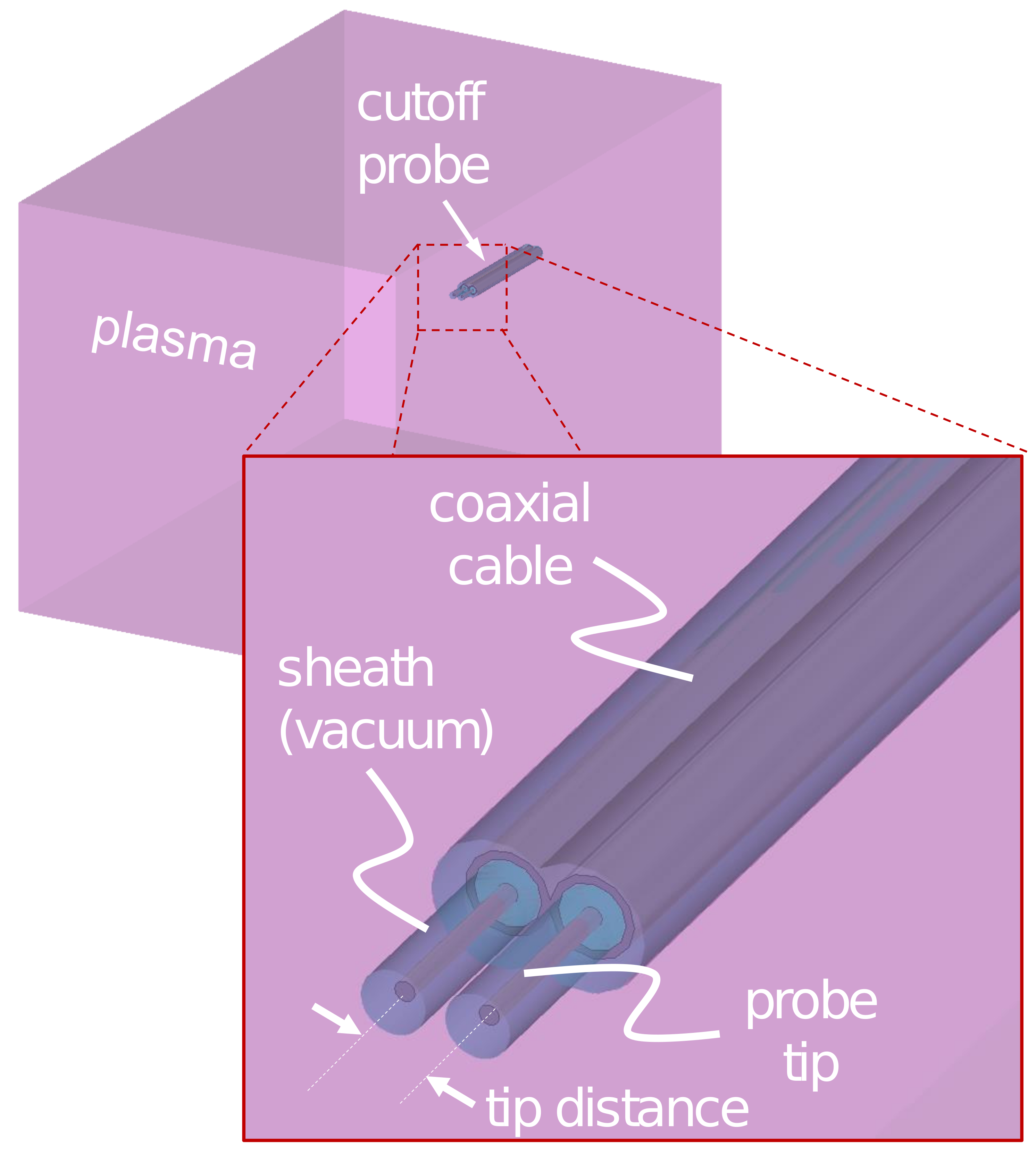
:1. Introduction
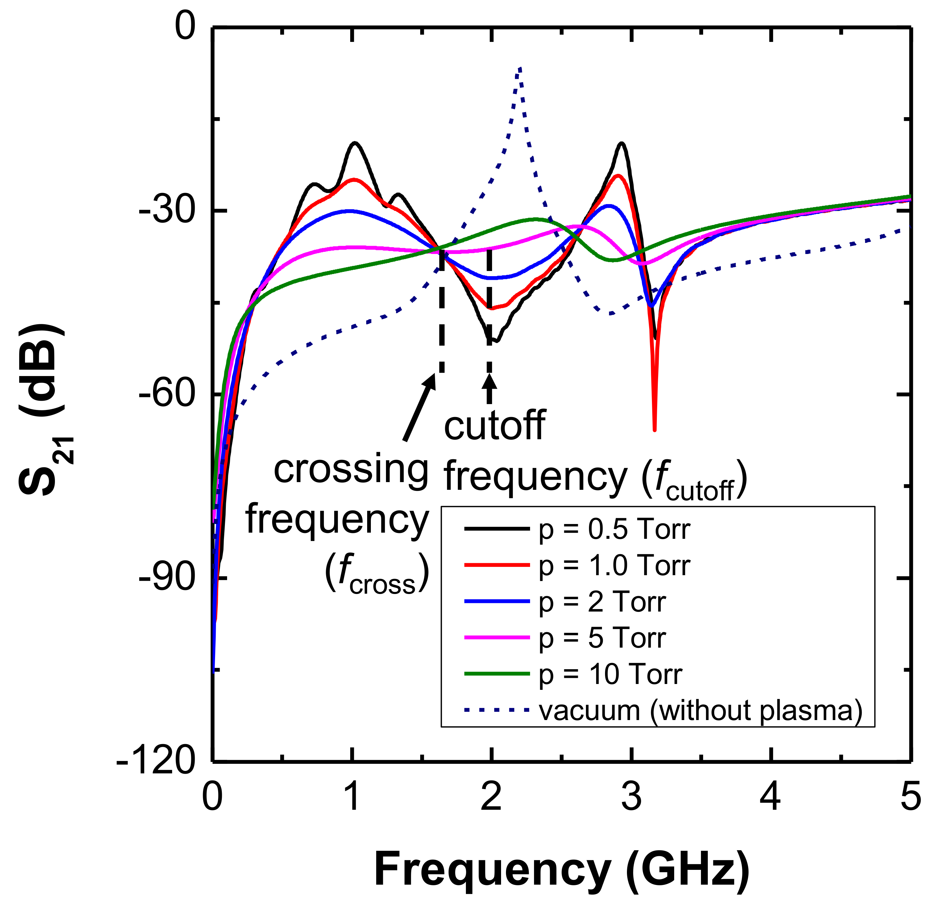
2. Simulation Demonstration
3. Experimental Demonstration and Circuit Model Analysis
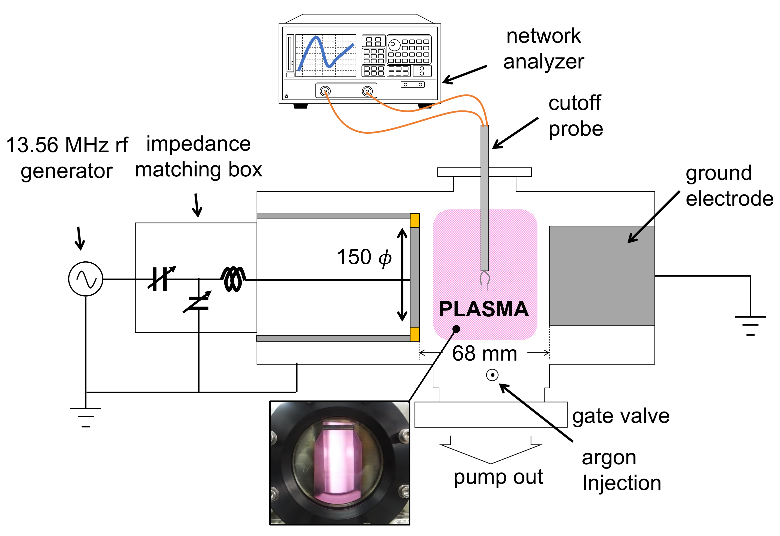
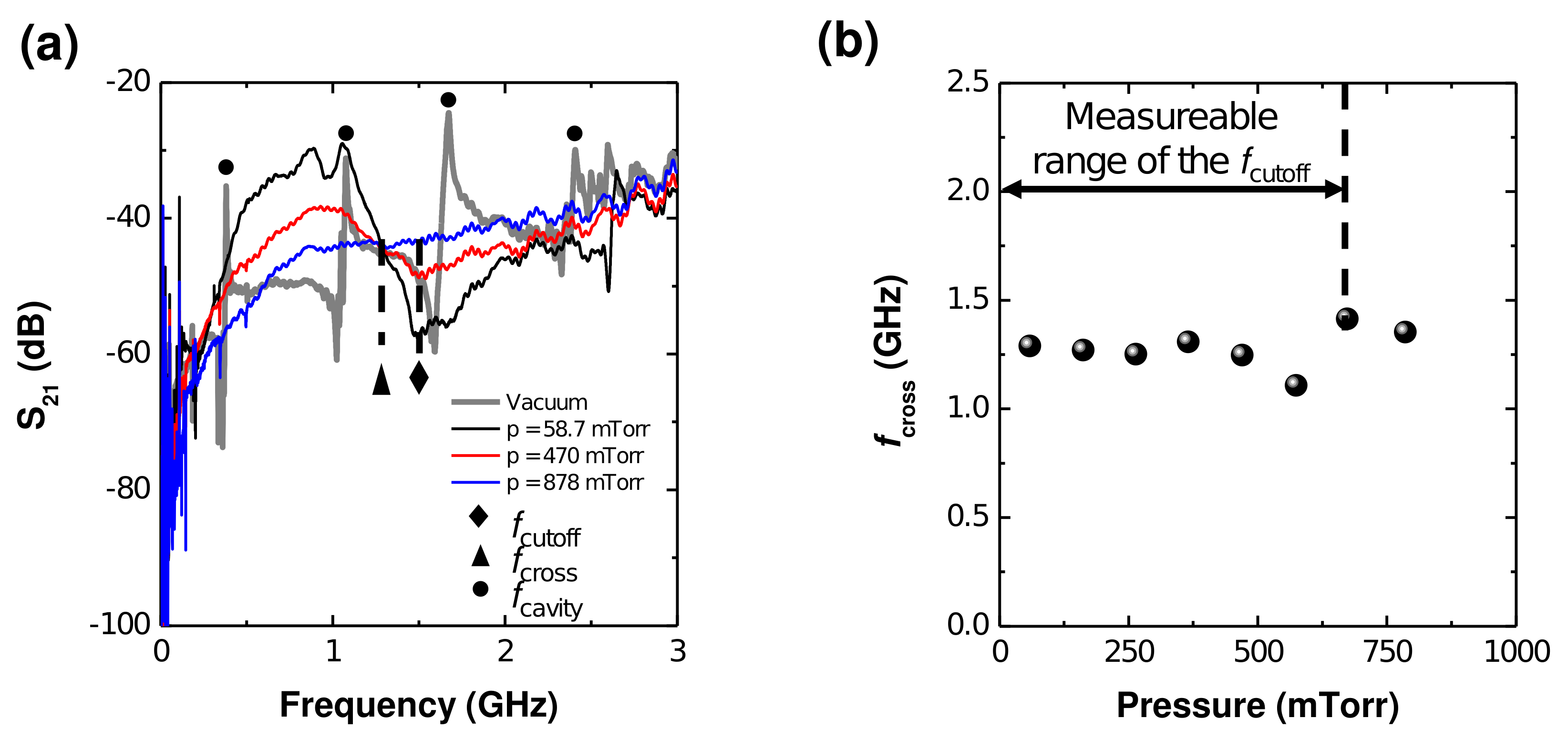
3.1. Experimental Demonstration
3.2. Circuit Model Analysis
4. Conclusions
Author Contributions
Funding
Institutional Review Board Statement
Informed Consent Statement
Data Availability Statement
Conflicts of Interest
References
- Adamovich, I.; Baalrud, S.D.; Bogaerts, A.; Bruggeman, P.J.; Cappelli, M.; Colombo, V.; Czarnetzki, U.; Ebert, U.; Eden, J.G. The 2017 Plasma Roadmap: Low temperature plasma science and technology. J. Phys. D Appl. Phys. 2017, 50, 323001. [Google Scholar] [CrossRef]
- Bogaerts, A.; Tu, X.; Whitehead, J.C.; Centi, G.; Lefferts, L.; Guaitella, O.; Azzolina-Jury, F.; Kim, H.; Murphy, A.B.; Schneider, W.F. The 2020 plasma catalysis roadmap. J. Phys. D Appl. Phys. 2020, 53, 443001. [Google Scholar] [CrossRef]
- Ishikawa, K.; Karahashi, K.; Ishijima, T.; Cho, S.I.I.; Elliott, S.; Hausmann, D.; Mocuta, D.; Wilson, A.; Kinoshita, K. Progress in nanoscale dry processes for fabrication of high-aspect-ratio features: How can we control critical dimension uniformity at the bottom? Jpn. J. Appl. Phys. 2018, 57, 06JA01. [Google Scholar] [CrossRef]
- Donnelly, V.M.; Kornblit, A. Plasma etching: Yesterday, today, and tomorrow. J. Vac. Sci. Technol. 2013, 31, 050825. [Google Scholar] [CrossRef] [Green Version]
- Cho, C.; You, K.; Kim, S.; Lee, Y.; Lee, J.; You, S. Characterization of SiO2 Etching Profiles in Pulse-Modulated Capacitively Coupled Plasmas. Materials 2021, 14, 5036. [Google Scholar] [CrossRef] [PubMed]
- Seong, I.H.; Lee, J.J.; Cho, C.H.; Lee, Y.S.; Kim, S.J.; You, S.J. Characterization of SiO2 Over Poly-Si Mask Etching in Ar/C4F8 Capacitively Coupled Plasma. Appl. Sci. Converg. Technol. 2021, 30, 176–182. [Google Scholar] [CrossRef]
- Lee, Y.; Seong, I.; Lee, J.; Lee, S.; Cho, C.; Kim, S.; You, S. Various evolution trends of sample thickness in fluorocarbon film deposition on SiO2. J. Vac. Sci. Technol. A 2022, 40, 013001. [Google Scholar] [CrossRef]
- Lee, H.; Chung, C. Electron heating and control of electron energy distribution for the enhancement of the plasma ashing processing. Plasma Sources Sci. Technol. 2015, 24, 024001. [Google Scholar] [CrossRef]
- Susa, Y.; Ohtake, H.; Jianping, Z.; Chen, L.; Nozawa, T. Characterization of CO2 plasma ashing for less low-dielectric-constant film damage. J. Vac. Sci. Technol. A 2015, 33, 061307. [Google Scholar] [CrossRef]
- Aizawa, T.; Shimada, T.; Sakurai, T.; Nakano, Y.; Tanaka, Y.; Uesugi, Y.; Ishijima, T. Improved Uniformity of Photoresist Ashing for a Half-Inch Wafer with Double U-shaped Antenna Structure in a Microwave-Excited Water Vapor Plasma. J. Photopolym. Sci. Technol. 2021, 34, 5. [Google Scholar] [CrossRef]
- Thedjoisworo, B.; Cheung, D.; Crist, V. Comparison of the effects of downstream H2- and O2-based plasmas on the removal of photoresist, silicon, and silicon nitride. J. Vac. Sci. Technol. B 2013, 31, 021206. [Google Scholar] [CrossRef]
- Profijt, H.B.; Potts, S.E.; van de Sanden, M.C.M.; Kessels, W.M.M. Plasma-Assisted Atomic Layer Deposition: Basics, Opportunities, and Challenges. J. Vac. Sci. Technol. A 2011, 29, 050801. [Google Scholar] [CrossRef] [Green Version]
- Kim, H.; Oh, I. Review of plasma-enhanced atomic layer deposition: Technical enabler of nanoscale device fabrication. Jpn. J. Appl. Phys. 2014, 53, 03DA01. [Google Scholar] [CrossRef]
- Potts, S.E.; Keuning, W.; Langereis, E.; Dingemans, G.; van de Sanden, M.C.M.; Kessels, W.M.M. Low Temperature Plasma-Enhanced Atomic Layer Deposition of Metal Oxide Thin Films. J. Electrochem. Soc. 2010, 157, P66–P74. [Google Scholar] [CrossRef]
- King, S.W. Plasma enhanced atomic layer deposition of SiNx:H and SiO2. J. Vac. Sci. Technol. A 2011, 29, 041501. [Google Scholar] [CrossRef]
- Lee, D.; Wan, Z.; Bae, J.; Lee, H.; Ahn, J.; Kim, S.; Kim, J.; Kwon, S. Plasma-enhanced atomic layer deposition of SnO2 thin films using SnCl4 and O2 plasma. Mater. Lett. 2016, 166, 163–166. [Google Scholar] [CrossRef]
- Hamedani, Y.; Macha, P.; Bunning, T.J.; Naik, R.R.; Vasudev, M.C. Plasma-Enhanced Chemical Vapor Deposition: Where we are and the Outlook for the Future. In Chemical Vapor Deposition, Recent Advances and Applications in Optical, Solar Cells and Solid State Devices; Sudheer Neralla; IntechOpen: London, UK, 2016; pp. 247–251. [Google Scholar]
- Vasudev, M.C.; Anderson, K.D.; Bunning, T.J.; Tsukruk, V.V.; Naik, R.R. Exploration of Plasma-Enhanced Chemical Vapor Deposition as a Method for Thin-Film Fabrication with Biological Applications. ASC Appl. Mater. Interfaces 2013, 5, 3983–3994. [Google Scholar] [CrossRef]
- Lieberman, M.A.; Lichtenberg, A.J. Principles of Plasma Discharges and Materials Processing, 2nd ed.; Wiley&Sons. Inc.: Hobken, NJ, USA, 2005; pp. 1–22. [Google Scholar]
- Marchack, N.; Buzi, L.; Farmer, D.B.; Miyazoe, H.; Papalia, J.M.; Yan, H.; Totir, G.; Engelmann, S.U. Plasma processing for advanced microelectronics beyond CMOS. J. Appl. Phys. 2021, 130, 080901. [Google Scholar] [CrossRef]
- Brault, P. Multiscale Molecular Dynamics Simulation of Plasma Processsing: Application to Plasma Sputtering. Front. Phys. 2018, 6, 59. [Google Scholar] [CrossRef]
- Denpoh, K.; Moroz, P.; Kato, T.; Matsukuma, M. Multiscale plasma and feature profile simulations of plasma enhanced chemical vapor deposition and atomic layer deposition processes for titanium thin film fabrication. Jpn. J. Appl. Phys. 2020, 59, SHHB02. [Google Scholar] [CrossRef]
- Becker, M.; Sierka, M. Atomistic Simulations of Plasma-Enhanced Atomic Layer Deposition. Materials 2019, 12, 2605. [Google Scholar] [CrossRef] [PubMed] [Green Version]
- Carbone, E.; Graef, W.; Hagelaar, G.; Boer, D.; Hopkins, M.M.; Stephens, J.C.; Yee, B.T.; Pancheshyi, S.; van Dijk, J.; Pitchford, L. Data Needs for Modeling Low-Temperature Non-equilibrium Plasmas: The LXCat Project, History, Perspectives and a Tutorial. Atoms 2021, 9, 16. [Google Scholar] [CrossRef]
- Rudenko, K.V. Diagnostics of Plasma Processes in Micro- and Nanoelectronics. High Energy Chem. 2009, 43, 3. [Google Scholar] [CrossRef]
- Creatore, M.; Palumbo, F.; d’Agostion, R. Deposition of SiOx Films from Hexamethyldisiloxane/Oxygen Radiofrequency Glow Discharges: Process Optimization by Plasma Diagnostics. Plasmas Polym. 2002, 7, 3. [Google Scholar] [CrossRef]
- Kirner, S.; Gabriel, O.; Stannowski, B.; Rech, B.; Schlatmann, R. The growth of microcrystalline silicon oxide thin films studied by in situ plasma diagnostics. Appl. Phys. Lett. 2013, 102, 051906. [Google Scholar] [CrossRef]
- Mackus, A.J.M.; Heil, S.B.S.; Langereis, E.; Knoops, H.C.M.; van de Sanden, M.C.M.; Kessels, W.M.M. Optical emission spectroscopy as a tool for studying, optimizing, and monitoring plasma-assisted atomic layer deposition processes. J. Vac. Sci. Technol. A 2010, 28, 1. [Google Scholar] [CrossRef] [Green Version]
- Seman, M.; Wolden, C.A. Investigation of the role of plasma conditions on the deposition rate and electrochromic performance of tungsten oxide thin films. J. Vac. Sci. Technol. A 2003, 21, 6. [Google Scholar] [CrossRef]
- Gopikishan, S.; Banerjee, I.; Bogle, K.A.; Das, A.K.; Pathak, A.P.; Mahapatra, S.K. Paschen curve approach to investigate electron density and deposition rate of Cu in magnetron sputtering system. Radiat. Eff. Deffects Solids 2016, 171, 999–1005. [Google Scholar] [CrossRef]
- Cherrington, B.E. The use of electrostatic probes for plasma diagnostics—A review. Plasma Chem. Plasma Process. 1982, 2, 113–140. [Google Scholar] [CrossRef]
- Lobbia, R.B.; Beal, B.E. Recommended Practice for Use of Langmuir Probes in Electric Propulsion Testing. J. Propuls. Power 2017, 33, 3. [Google Scholar] [CrossRef]
- Engeln, R.; Klarenaar, B.; Guaitella, O. Foundations of optical diagnostics in low-temperature plasmas. Plasma Sources Sci. Technol. 2020, 29, 063001. [Google Scholar] [CrossRef]
- Belostotskiy, S.G.; Khandelwal, R.K.; Wang, Q.; Donnelly, V.M.; Economou, D.J.; Sadeghi, N. Measurement of electron temperature and density in an argon microdischarge by laser Thomson scattering. Appl. Phys. Lett. 2008, 92, 221507. [Google Scholar] [CrossRef] [Green Version]
- Kim, J.; Seong, D.; Lim, J.; Chung, K. Plasma frequency measurements for absolute plasma density by means of wave cutoff method. Appl. Phys. Lett. 2003, 83, 23. [Google Scholar] [CrossRef]
- Piejak, R.B.; Godyak, V.A.; Garner, R.; Alexandrovich, M.B.; Sternber, N. The hairpin resonator: A plasma density measuring technique revisited. J. Appl. Phys. 2004, 95, 7. [Google Scholar] [CrossRef]
- Blackwell, D.D.; Walker, D.N.; Amatucci, W.E. Measurement of absolute electron density with a plasma impedance probe. Rev. Sci. Instrum. 2005, 76, 023503. [Google Scholar] [CrossRef]
- Dine, S.; Booth, J.-P.; Curley, G.A.; Corr, C.S.; Jolly, J.; Guillon, J. A novel technique for plasma density measurement using surface-wave transmission spectra. Plasma Sources Sci. Technol. 2005, 14, 777–786. [Google Scholar] [CrossRef]
- Chen, F.F. Lecture Notes on Langmuir Probe Diagnostics. In Proceedings of the The 30th International Conference on Plasma Science, Jeju, Korea, 2–5 June 2003. [Google Scholar]
- Kim, J.-H.; Choi, S.-C.; Shin, Y.-H.; Chung, K.-H. Wave cutoff method to measure absolute electron density in cold plasma. Rev. Sci. Instrum. 2004, 75, 2706–2710. [Google Scholar] [CrossRef]
- You, K.H.; You, S.J.; Kim, D.W.; Na, B.K.; Seo, B.H.; Kim, J.H.; Seong, D.J.; Chang, H.-Y. Measurement of electron density using reactance cutoff probe. Phys. Plasmas 2016, 23, 053515. [Google Scholar] [CrossRef]
- Sugai, H.; Nakamura, K. Recent innovations in microwave probes for reactive plasma diagnostics. Jpn. J. Appl. Phys. 2019, 58, 060101. [Google Scholar] [CrossRef]
- Kim, D.W.; You, S.J.; Kim, J.H.; Chang, H.Y.; Oh, W.Y. Computational comparative study of microwave probes for plasma density measurement. Plasma Sources Sci. Technol. 2016, 25, 035026. [Google Scholar] [CrossRef]
- Styrnoll, T.; Harhausen, J.; Lapke, M.; Storch, R.; Brinkmann, R.P.; Foest, R.; Ohl, A.; Awakowicz, P. Process diagnostics and monitoring using the multipole resonance probe in an inhomogeneous plasma for ion-assisted deposition of optical coatings. Plasma Sources Sci. Technol. 2013, 22, 045008. [Google Scholar] [CrossRef]
- Ogawa, D.; Nakamura, K.; Sugai, H. Experimental validity of double-curling probe method in film-depositing plasma. Plasma Sources Sci. Technol. 2021, 30, 085009. [Google Scholar] [CrossRef]
- Xu, J.; Nakamura, K.; Zhang, Q.; Sugai, H. Simulation of resistive microwave resonator probe for high-pressure plasma diagnostics. Plasma Sources Sci. Technol. 2009, 18, 045009. [Google Scholar] [CrossRef]
- Jun, H.; Lee, Y.; Na, B.; Chang, H. Pressure limitation of electron density measurement using a wave-cutoff method in weakly ionized plasmas. Phys. Plasmas 2008, 15, 124504. [Google Scholar] [CrossRef]
- Kim, D.W.; You, S.J.; Na, B.K.; Kim, J.H.; Chang, H.Y. An analysis on transmission microwave frequency spectrum of cut-off probe. Appl. Phys. Lett. 2011, 99, 131502. [Google Scholar] [CrossRef] [Green Version]
- Kim, S.J.; Lee, J.J.; Kim, D.W.; Kim, J.H.; You, S.J. A transmission line model of the cutoff probe. Plasma Sources Sci. Technol. 2019, 28, 055014. [Google Scholar] [CrossRef]
- Kim, D.W.; You, S.J.; Kwon, J.H.; You, K.H.; Seo, B.H.; Kim, J.H.; Yoon, J.-S.; Oh, W.Y. Reproducibility of the cutoff probe for the measurement of electron density. Phys. Plasmas 2016, 23, 063501. [Google Scholar] [CrossRef]
- Seo, B.; Kim, D.; Kim, J.; You, S. Investigation of reliability of the cutoff probe by a comparison with Thomson scattering in high density processing plasmas. Phys. Plasmas 2017, 24, 123502. [Google Scholar] [CrossRef] [Green Version]
- Kim, D.-W.; Youb, S.-J.; Kim, J.-H.; Seong, D.-J.; Chang, H.-Y.; Oh, W.-Y. Computational study on reliability of sheath width measurement by the cutoff probe in low pressure plasmas. In Proceedings of the 1st EPS Conference on Plasma Diagnostics (1STECPD), Frascati, Rome, Italy, 14–17 April 2015. [Google Scholar]
- Kim, D.W.; You, S.J.; Kim, S.J.; Kim, J.H.; Oh, W.Y. Two-resonance probe for measuring electron density in low-pressure plasmas. Plasma Sources Sci. Technol. 2017, 26, 045015. [Google Scholar] [CrossRef]
- Godyak, V.A.; Piejak, R.B.; Alexandrovich, B.M. Measurements of electron energy distribution in low-pressure RF discharges. Plasma Sources Sci. Technol. 1992, 1, 36–58. [Google Scholar] [CrossRef]
- Lafleur, T.; Chabert, P.; Booth, J.P. Electron heating in capacitively coupled plasmas revisited. Plasma Sources Sci. Technol. 2014, 23, 035010. [Google Scholar] [CrossRef]
- Na, B.; Kim, D.; Kwon, J.; Chang, H.; Kim, J.; You, S. Computational characterization of cutoff probe system for the measurement of electron density. Phys. Plasmas 2012, 19, 053504. [Google Scholar] [CrossRef]
- Na, B.; You, K.; Kim, D.; Chang, H.; You, S.; Kim, J. Cutoff probe using Fourier analysis for electron density measurement. Rev. Sci. Instrum. 2012, 83, 013510. [Google Scholar] [CrossRef] [PubMed]
- Kim, D.W.; You, S.J.; Kim, J.H.; Chang, H.Y.; Yoon, J.-S.; Oh, W.Y. Measurement of effective sheath width around the cutoff probe based on electromagnetic simulation. Phys. Plasmas 2016, 23, 053516. [Google Scholar] [CrossRef]


Publisher’s Note: MDPI stays neutral with regard to jurisdictional claims in published maps and institutional affiliations. |
© 2022 by the authors. Licensee MDPI, Basel, Switzerland. This article is an open access article distributed under the terms and conditions of the Creative Commons Attribution (CC BY) license (https://creativecommons.org/licenses/by/4.0/).
Share and Cite
Kim, S.-j.; Lee, J.-j.; Lee, Y.-s.; Cho, C.-h.; You, S.-j. Crossing Frequency Method Applicable to Intermediate Pressure Plasma Diagnostics Using the Cutoff Probe. Sensors 2022, 22, 1291. https://doi.org/10.3390/s22031291
Kim S-j, Lee J-j, Lee Y-s, Cho C-h, You S-j. Crossing Frequency Method Applicable to Intermediate Pressure Plasma Diagnostics Using the Cutoff Probe. Sensors. 2022; 22(3):1291. https://doi.org/10.3390/s22031291
Chicago/Turabian StyleKim, Si-jun, Jang-jae Lee, Young-seok Lee, Chul-hee Cho, and Shin-jae You. 2022. "Crossing Frequency Method Applicable to Intermediate Pressure Plasma Diagnostics Using the Cutoff Probe" Sensors 22, no. 3: 1291. https://doi.org/10.3390/s22031291
APA StyleKim, S.-j., Lee, J.-j., Lee, Y.-s., Cho, C.-h., & You, S.-j. (2022). Crossing Frequency Method Applicable to Intermediate Pressure Plasma Diagnostics Using the Cutoff Probe. Sensors, 22(3), 1291. https://doi.org/10.3390/s22031291