
The Effect of Geometrical Overlap between Giant Magnetoresistance Sensor and Magnetic Flux Concentrators: A Novel Comb-Shaped Sensor for Improved Sensitivity


Abstract
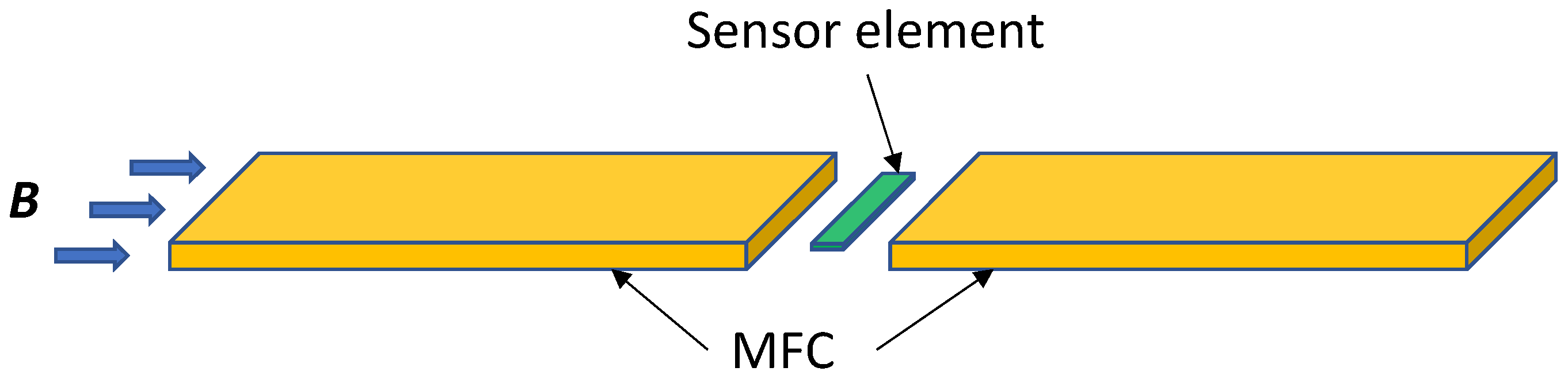
1. Introduction
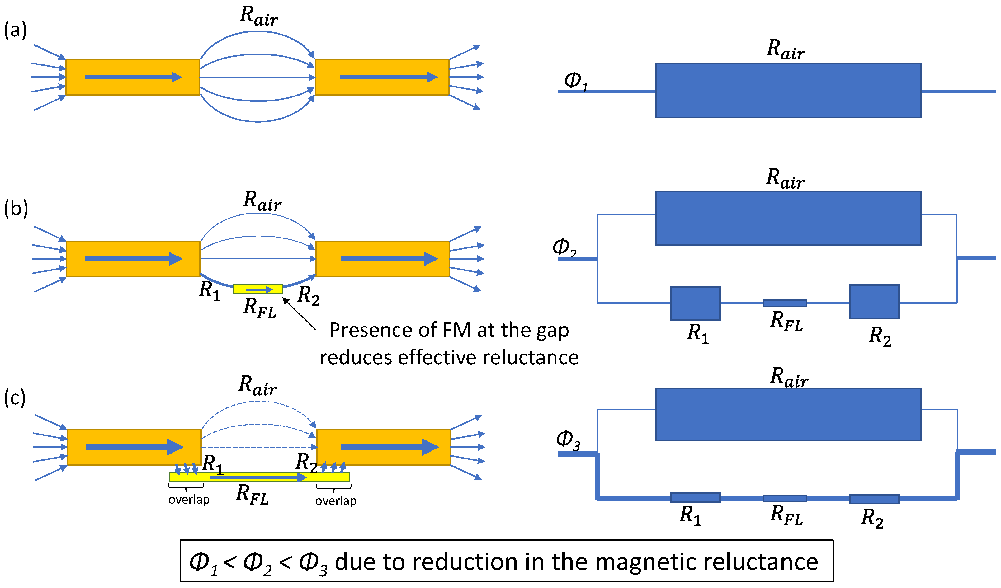
2. Magnetic Circuit in the MFC–FL System
3. Methods
3.1. Finite Element Method Simulations
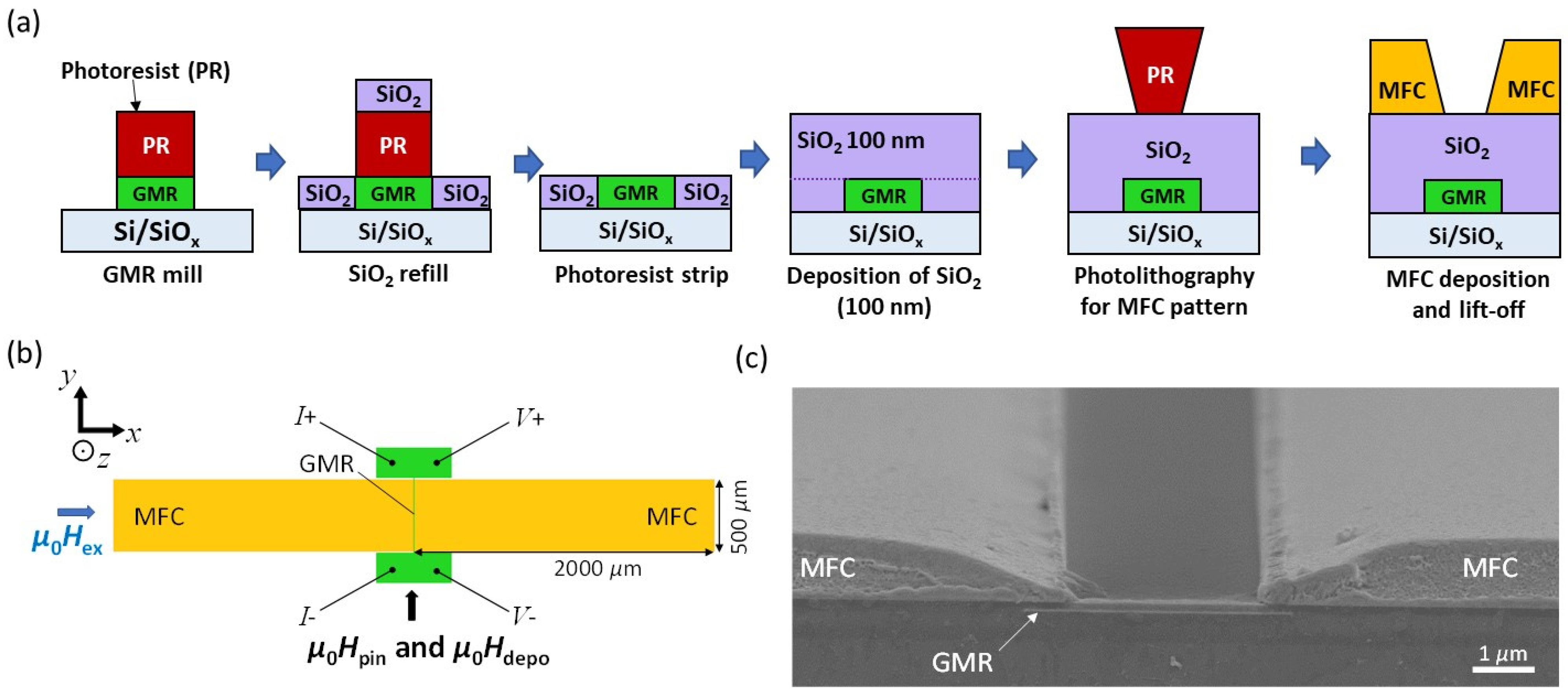
3.2. Experimental Procedures
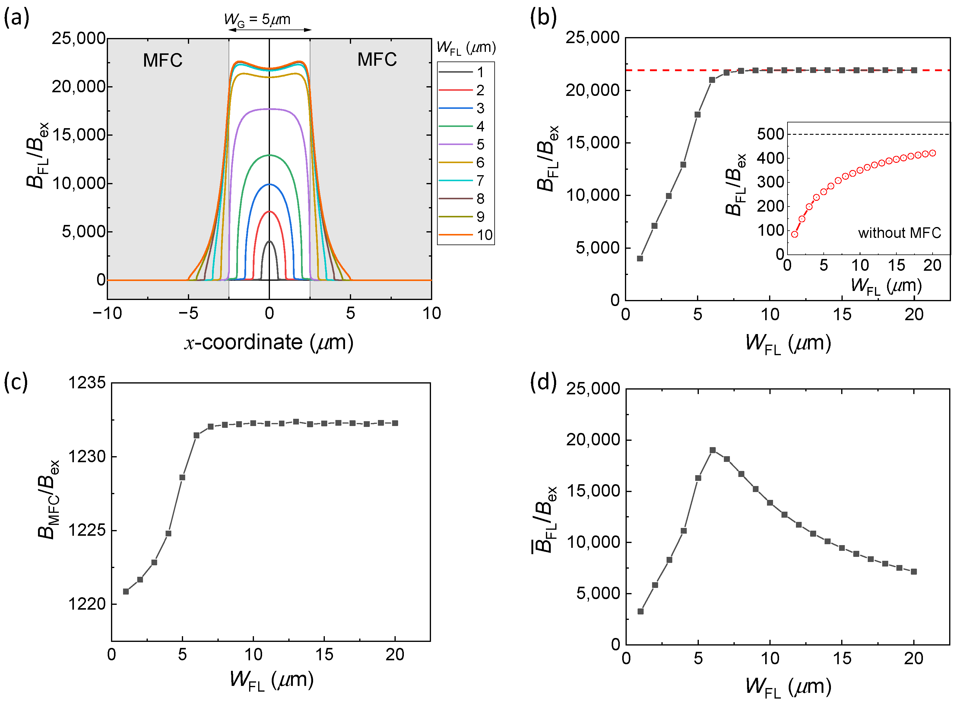
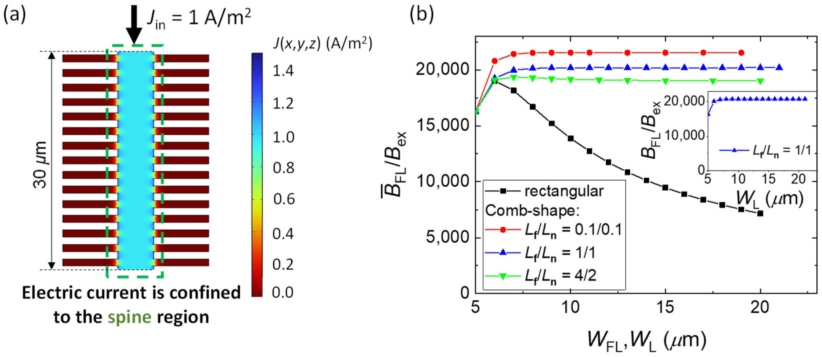
4. Results and Discussion: FEM Simulations
4.1. Rectangular FL
4.2. Comb-Shaped FL
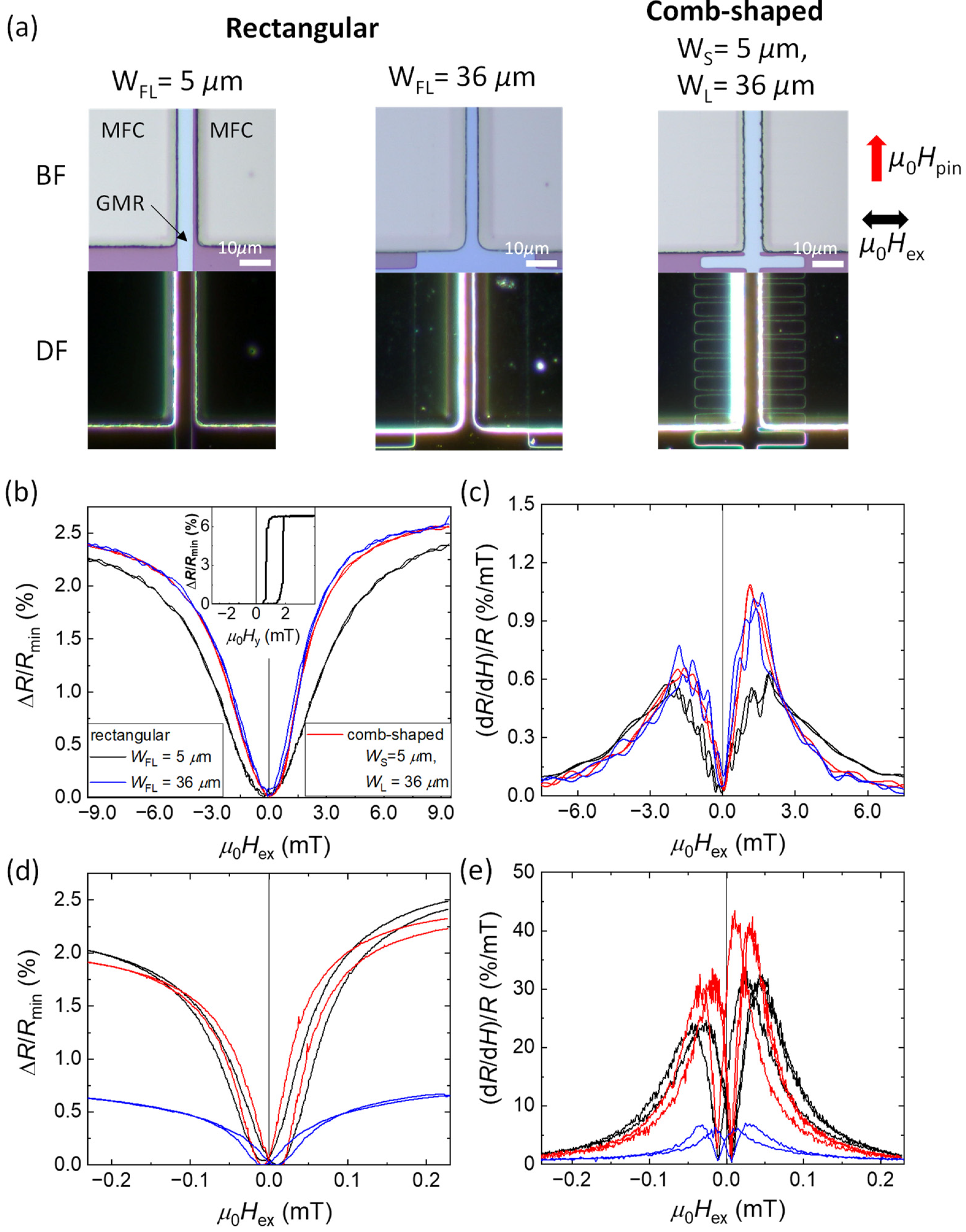
5. Results and Discussion: Experiments
6. Conclusions
Supplementary Materials
Author Contributions
Funding
Institutional Review Board Statement
Informed Consent Statement
Data Availability Statement
Acknowledgments
Conflicts of Interest
References
- Zheng, C.; Zhu, K.; de Freitas, S.C.; Chang, J.-Y.; Davies, J.E.; Eames, P.; Freitas, P.P.; Kazakova, O.; Kim, C.; Leung, C.-W.; et al. Magnetoresistive Sensor Development Roadmap (Non-Recording Applications). IEEE Trans. Magn. 2019, 55, 0800130. [Google Scholar] [CrossRef]
- Reig, C.; Cubells-Beltrán, M.-D. Giant Magnetoresistance (GMR) Magnetometers. In High Sensit. Magnetometers. Smart Sensors, Meas. Instrum; Springer: Cham, Switzerland, 2017; pp. 225–252. [Google Scholar] [CrossRef]
- Cubells-Beltrán, M.-D.; Reig, C.; Madrenas, J.; De Marcellis, A.; Santos, J.; Cardoso, S.; Freitas, P.P. Integration of GMR Sensors with Different Technologies. Sensors 2016, 16, 939. [Google Scholar] [CrossRef] [PubMed]
- Application Notes for GMR Sensors, NVE Corp. (n.d.). Available online: https://www.nve.com/Downloads/apps.pdf (accessed on 30 October 2022).
- Davies, J.E.; Watts, J.D.; Novotny, J.; Huang, D.; Eames, P.G. Magnetoresistive sensor detectivity: A comparative analysis. Appl. Phys. Lett. 2021, 118, 062401. [Google Scholar] [CrossRef]
- Trisnanto, S.B.; Kasajima, T.; Akushichi, T.; Takemura, Y. Magnetic particle imaging using linear magnetization response-driven harmonic signal of magnetoresistive sensor. Appl. Phys. Express 2021, 14, 095001. [Google Scholar] [CrossRef]
- Blanchard, H.; De Montmollin, F.; Hubin, J.; Popovic, R. Highly sensitive Hall sensor in CMOS technology. Sens. Actuators A Phys. 2000, 82, 144–148. [Google Scholar] [CrossRef]
- Randjelovic, Z.; Kayal, M.; Popovic, R.; Blanchard, H. Highly sensitive Hall magnetic sensor microsystem in CMOS technology. IEEE J. Solid-State Circuits 2002, 37, 151–159. [Google Scholar] [CrossRef]
- Smith, N.; Jeffers, F.; Freeman, J. A high-sensitivity magnetoresistive magnetometer. J. Appl. Phys. 1991, 69, 5082–5084. [Google Scholar] [CrossRef]
- Shen, H.-M.; Hu, L.; Fu, X. Integrated Giant Magnetoresistance Technology for Approachable Weak Biomagnetic Signal Detections. Sensors 2018, 18, 148. [Google Scholar] [CrossRef]
- Coelho, P.; Leitao, D.C.; Antunes, J.; Cardoso, S.; Freitas, P.P. Spin Valve Devices with Synthetic-Ferrimagnet Free-Layer Displaying Enhanced Sensitivity for Nanometric Sensors. IEEE Trans. Magn. 2014, 50, 4401604. [Google Scholar] [CrossRef]
- Oogane, M.; Fujiwara, K.; Kanno, A.; Nakano, T.; Wagatsuma, H.; Arimoto, T.; Mizukami, S.; Kumagai, S.; Matsuzaki, H.; Nakasato, N.; et al. Sub-pT magnetic field detection by tunnel magneto-resistive sensors. Appl. Phys. Express 2021, 14, 123002. [Google Scholar] [CrossRef]
- He, G.; Zhang, Y.; Qian, L.; Xiao, G.; Zhang, Q.; Santamarina, J.C.; Patzek, T.; Zhang, X. PicoTesla magnetic tunneling junction sensors integrated with double staged magnetic flux concentrators. Appl. Phys. Lett. 2018, 113, 242401. [Google Scholar] [CrossRef]
- Pannetier, M.; Fermon, C.; Le Goff, G.; Simola, J.; Kerr, E. Femtotesla Magnetic Field Measurement with Magnetoresistive Sensors. Science 2004, 304, 1648–1650. [Google Scholar] [CrossRef]
- Edelstein, A.S.; Fischer, G.A.; Pedersen, M.; Nowak, E.R.; Cheng, S.F.; Nordman, C.A. Progress toward a thousandfold reduction in 1∕f noise in magnetic sensors using an ac microelectromechanical system flux concentrator (invited). J. Appl. Phys. 2006, 99, 08B317. [Google Scholar] [CrossRef]
- Che, Y.; Hu, J.; Pan, L.; Li, P.; Pan, M.; Chen, D.; Sun, K.; Zhang, X.; Du, Q.; Yu, Y.; et al. Magnetic flux modulation with electric controlled permeability for magnetoresistive sensor. AIP Adv. 2020, 10, 105032. [Google Scholar] [CrossRef]
- Lyu, H.; Liu, Z.; Wang, Z.; Yang, W.; Xiong, X.; Chen, J.; Zou, X. A high-resolution MEMS magnetoresistive sensor utilizing magnetic tunnel junction motion modulation driven by the piezoelectric resonator. Appl. Phys. Lett. 2022, 121, 123504. [Google Scholar] [CrossRef]
- Kikitsu, A.; Higashi, Y.; Kurosaki, Y.; Shirotori, S.; Nagatsuka, T.; Suzuki, K.; Terui, Y. Magnetic field microscope using high-sensitivity giant magneto-resistance sensor with AC field modulation. Jpn. J. Appl. Phys. 2022, 62, SB1007. [Google Scholar] [CrossRef]
- Zhang, X.; Bi, Y.; Chen, G.; Liu, J.; Li, J.; Feng, K.; Lv, C.; Wang, W. Influence of size parameters and magnetic field intensity upon the amplification characteristics of magnetic flux concentrators. AIP Adv. 2018, 8, 125222. [Google Scholar] [CrossRef]
- Yang, Y.; Liou, S.-H. Laminated magnetic film for micro magnetic flux concentrators. AIP Adv. 2021, 11, 035004. [Google Scholar] [CrossRef]
- Maspero, F.; Cuccurullo, S.; Mungpara, D.; Schwarz, A.; Bertacco, R. Impact of magnetic domains on magnetic flux concentrators. J. Magn. Magn. Mater. 2021, 535, 168072. [Google Scholar] [CrossRef]
- Marinho, Z.; Cardoso, S.; Chaves, R.; Ferreira, R.; Melo, L.V.; Freitas, P.P. Three dimensional magnetic flux concentrators with improved efficiency for magnetoresistive sensors. J. Appl. Phys. 2011, 109, 07E521. [Google Scholar] [CrossRef]
- Drljača, P.M.; Vincent, F.; Besse, P.-A.; Popović, R.S. Design of planar magnetic concentrators for high sensitivity Hall devices. Sens. Actuators A Phys. 2002, 97–98, 10–14. [Google Scholar] [CrossRef]
- Valadeiro, J.; Leitao, D.C.; Cardoso, S.; Freitas, P.P. Improved Efficiency of Tapered Magnetic Flux Concentrators with Double-Layer Architecture. IEEE Trans. Magn. 2017, 53, 4003805. [Google Scholar] [CrossRef]
- AC/DC Module User’s Guide; COMSOL Multiphysics® v. 6.1; COMSOL AB: Stockholm, Sweden, 2022; Available online: https://doc.comsol.com/6.1/doc/com.comsol.help.acdc/ACDCModuleUsersGuide.pdf (accessed on 1 October 2022).
- Technical Datasheet: AZ nLOF 2000 Series Negative Tone Photoresists for Single Layer Lift-Off, (n.d.). Available online: https://www.microchemicals.com/micro/tds_az_nlof2000_series.pdf (accessed on 15 November 2022).
- Shirotori, S.; Kikitsu, A.; Higashi, Y.; Kurosaki, Y.; Iwasaki, H. Symmetric Response Magnetoresistance Sensor with Low 1/f Noise by Using an Antiphase AC Modulation Bridge. IEEE Trans. Magn. 2020, 57, 4000305. [Google Scholar] [CrossRef]


| FL Shape (in μm) | Degree of Confinement of Electric Current (Ispine/Itotal) | with MFC | without MFC | MFC Gain |
|---|---|---|---|---|
| Comb shape, WL = 15 Lf = Ln= 0.1 | 0.992 | 21,550 | 340 | 63 |
| Comb shape, WL = 15 Lf = Ln = 1.0 | 0.952 | 20,200 | 338 | 60 |
| Comb shape, WL = 15 Lf = 4, Ln = 2 | 0.787 | 19,050 | 359 | 53 |
| Rectangular WFL = 5 | (Igap/Itotal =) 1.0 | 16,300 | 218 | 75 |
| Rectangular WFL = 15 | (Igap/Itotal =) 0.333 | 9470 | 345 | 27 |
| Device | Max Sensitivity without MFC (%/mT) | Max Sensitivity with MFC (%/mT) | MFC Gain | ||||
|---|---|---|---|---|---|---|---|
| −Smax | +Smax | Avg. Smax | −Smax | +Smax | Avg. Smax | ||
| Rectangular WFL = 5 | 0.6 | 0.6 | 0.6 | 24 | 32 | 28 | 47 |
| Rectangular WFL = 36 | 0.7 | 1 | 0.85 | 6 | 6 | 6 | 7 |
| Comb shape WL = 36, WS = 5 | 0.7 | 1 | 0.85 | 31 | 42 | 36.5 | 43 |
Publisher’s Note: MDPI stays neutral with regard to jurisdictional claims in published maps and institutional affiliations. |
© 2022 by the authors. Licensee MDPI, Basel, Switzerland. This article is an open access article distributed under the terms and conditions of the Creative Commons Attribution (CC BY) license (https://creativecommons.org/licenses/by/4.0/).
Share and Cite
Kulkarni, P.D.; Iwasaki, H.; Nakatani, T. The Effect of Geometrical Overlap between Giant Magnetoresistance Sensor and Magnetic Flux Concentrators: A Novel Comb-Shaped Sensor for Improved Sensitivity. Sensors 2022, 22, 9385. https://doi.org/10.3390/s22239385
Kulkarni PD, Iwasaki H, Nakatani T. The Effect of Geometrical Overlap between Giant Magnetoresistance Sensor and Magnetic Flux Concentrators: A Novel Comb-Shaped Sensor for Improved Sensitivity. Sensors. 2022; 22(23):9385. https://doi.org/10.3390/s22239385
Chicago/Turabian StyleKulkarni, Prabhanjan D., Hitoshi Iwasaki, and Tomoya Nakatani. 2022. "The Effect of Geometrical Overlap between Giant Magnetoresistance Sensor and Magnetic Flux Concentrators: A Novel Comb-Shaped Sensor for Improved Sensitivity" Sensors 22, no. 23: 9385. https://doi.org/10.3390/s22239385
APA StyleKulkarni, P. D., Iwasaki, H., & Nakatani, T. (2022). The Effect of Geometrical Overlap between Giant Magnetoresistance Sensor and Magnetic Flux Concentrators: A Novel Comb-Shaped Sensor for Improved Sensitivity. Sensors, 22(23), 9385. https://doi.org/10.3390/s22239385