
A Fully Integrated, Power-Efficient, 0.07–2.08 mA, High-Voltage Neural Stimulator in a Standard CMOS Process


Abstract
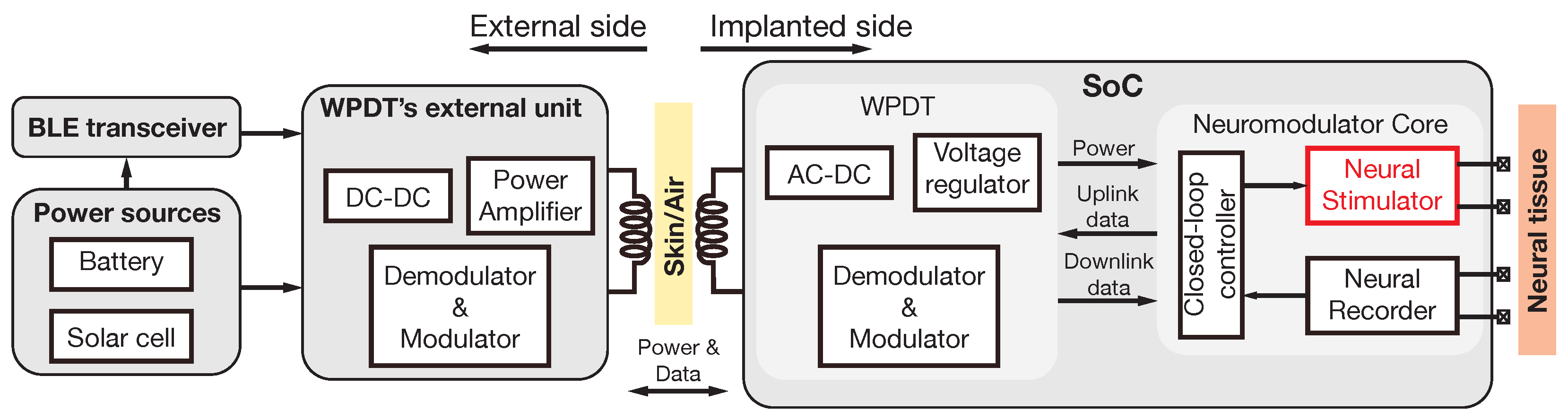
:1. Introduction
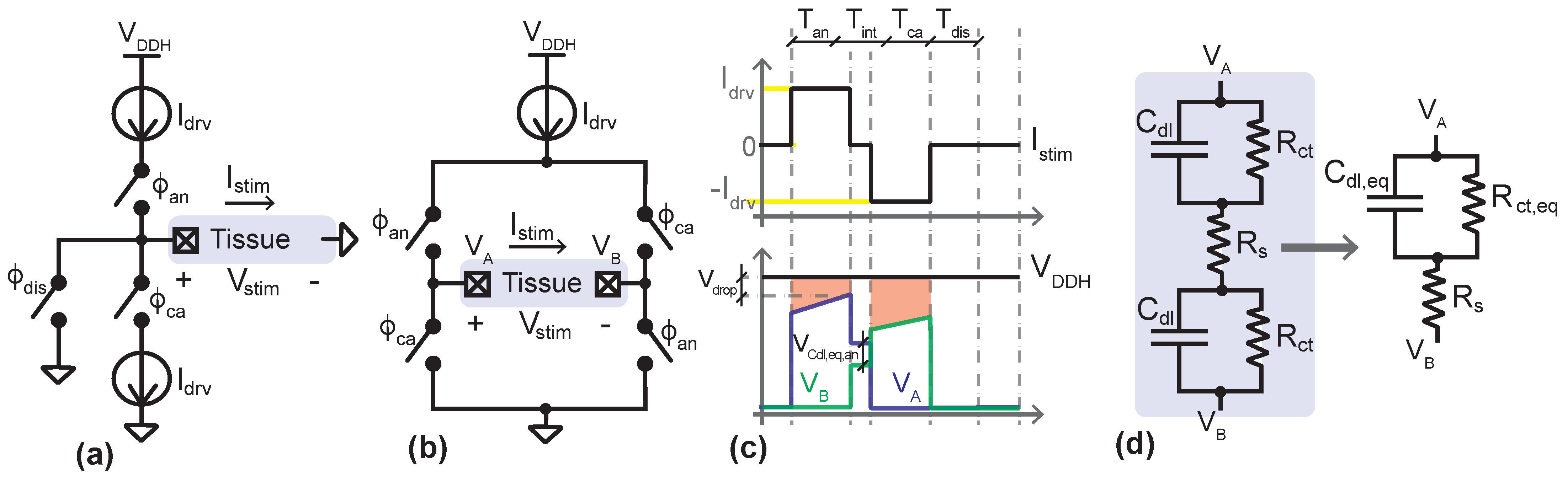
2. Current-Mode Biphasic Stimulation: Compliance Voltage and Power Efficiency
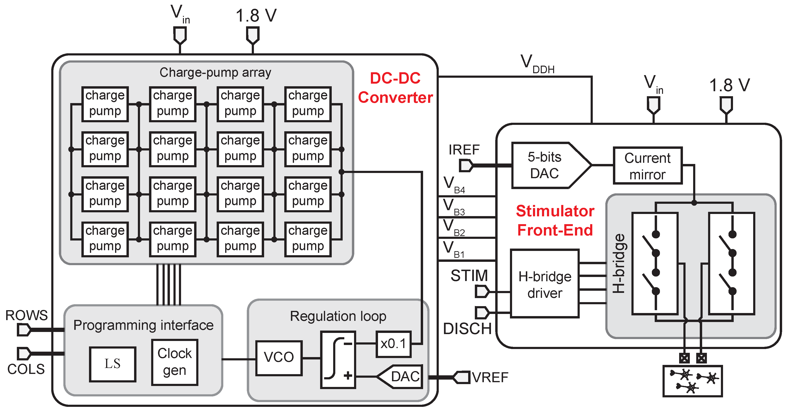
3. System Architecture and Circuit Design
3.1. Switched-Capacitor DC-DC Converter
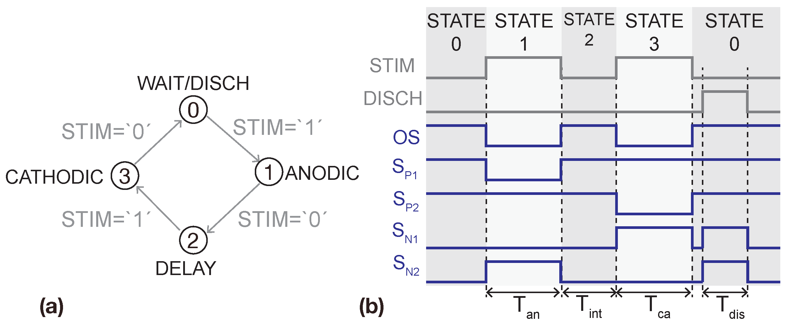
3.2. H-Bridge
3.3. DAC and Current Mirror
3.4. H-Bridge Driver
4. Experimental Results
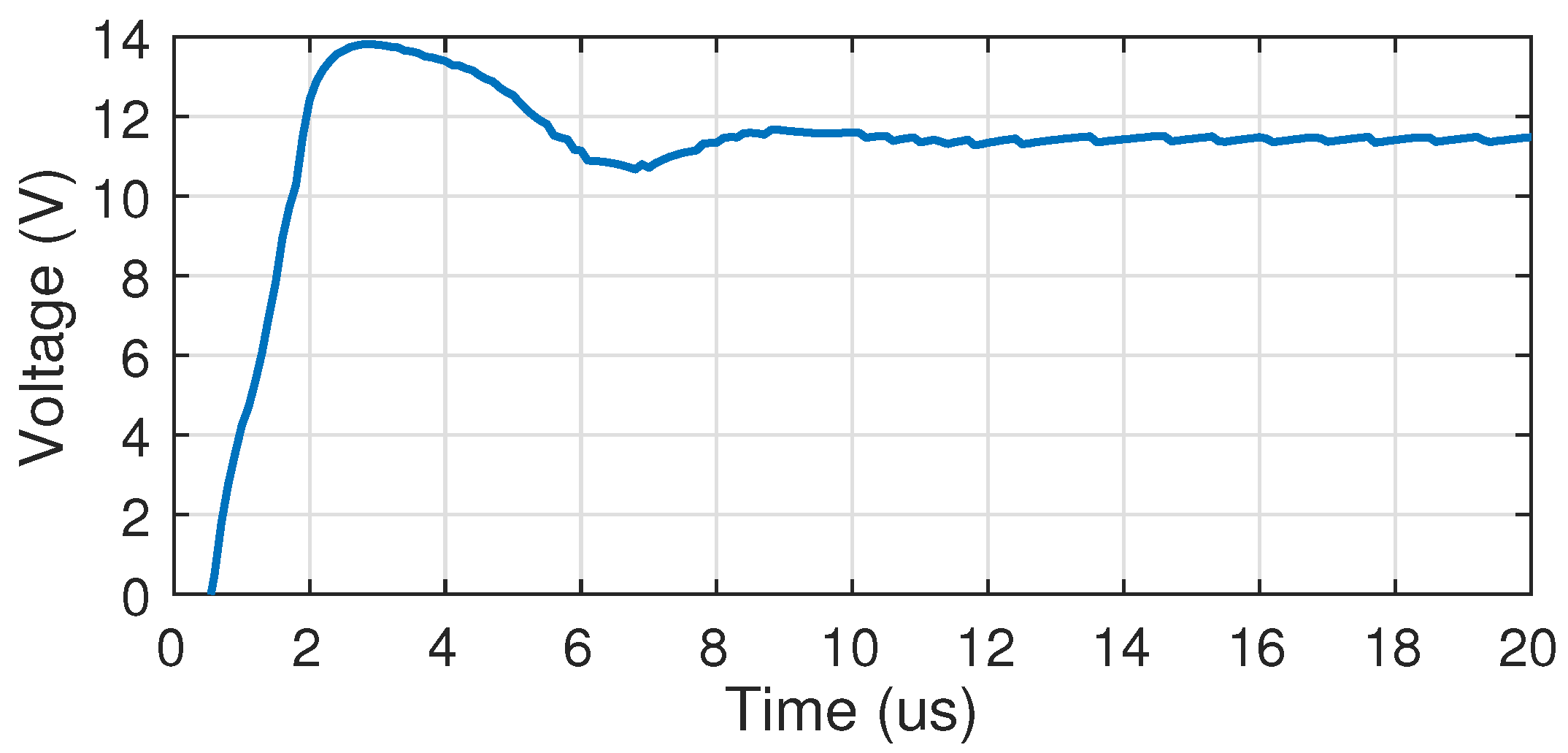
4.1. Electrical Characterization
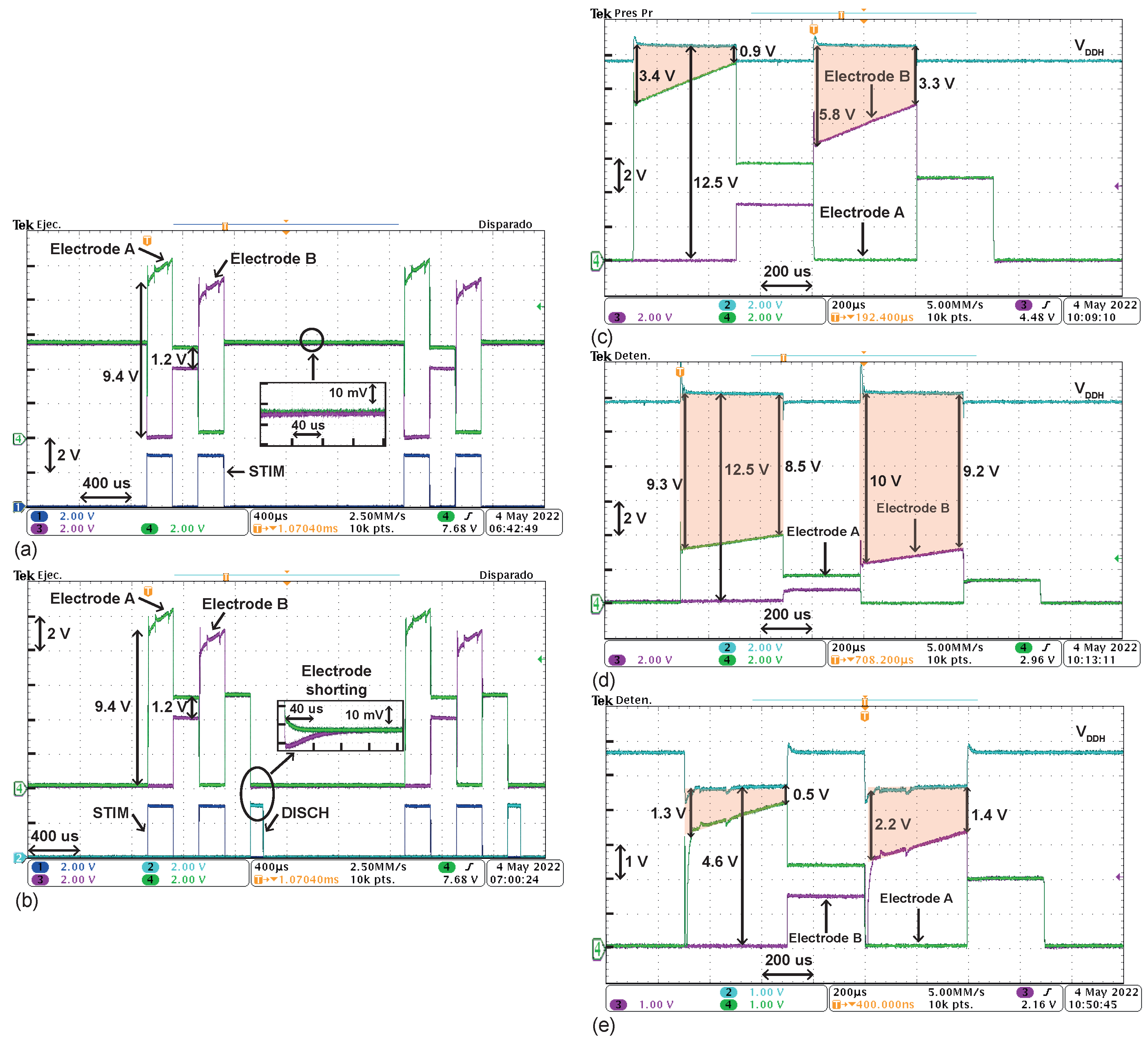
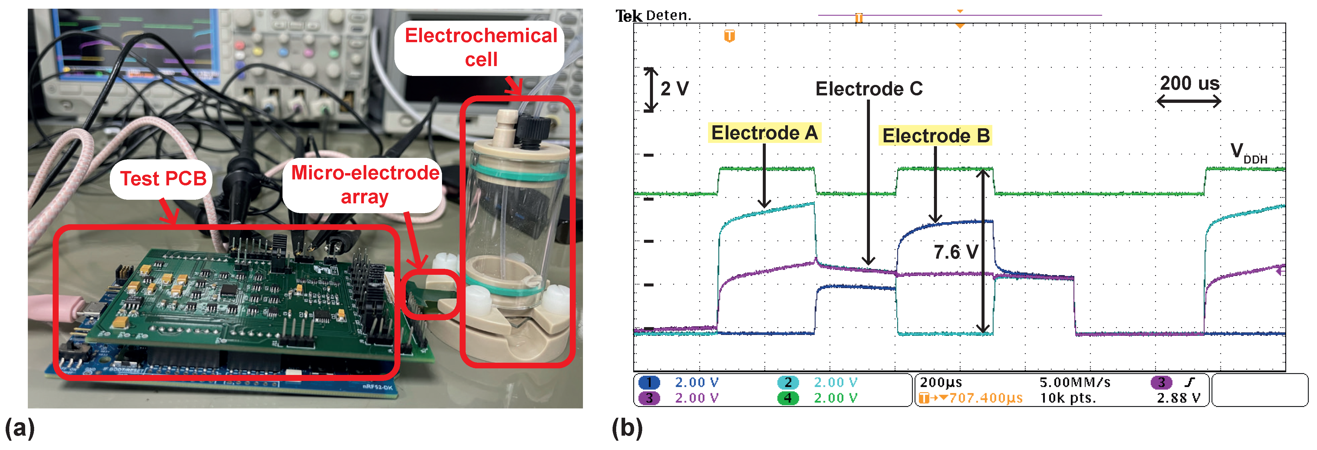
4.2. Measurements on a Phosphate-Buffered Saline (PBS) Solution
4.3. State-of-the-Art Comparison
5. Conclusions
Author Contributions
Funding
Institutional Review Board Statement
Informed Consent Statement
Data Availability Statement
Conflicts of Interest
Abbreviations
| HV | high-voltage |
| LV | low-voltage |
| ETI | electrode–tissue interface |
| BLE | Bluetooth Low Energy |
| WPDT | Wireless Power and Data Transfer |
| SoC | System on Chip |
| HCVC | high-compliance voltage cell |
| DAC | digital-to-analog converter |
| FLS | floating level-shifters |
| DNL | differential non-linearity |
| INL | integral non-linearity |
| LSB | least-significant bit |
| SPI | serial peripheral interface |
References
- Lefaucheur, J.P. Methods of Therapeutic Cortical Stimulation. Neurophysiol. Clin./Clin. Neurophysiol. 2009, 39, 1–14. [Google Scholar] [CrossRef] [PubMed]
- Oluigbo, C.O.; Salma, A.; Rezai, A.R. Deep Brain Stimulation for Neurological Disorders. IEEE Rev. Biomed. Eng. 2012, 5, 88–99. [Google Scholar] [CrossRef] [PubMed]
- Hickey, P.; Stacy, M. Deep Brain Stimulation: A Paradigm Shifting Approach to Treat Parkinson’s Disease. Front. Neurosci. 2016, 10, 173. [Google Scholar] [CrossRef] [PubMed]
- Koeglsperger, T.; Palleis, C.; Hell, F.; Mehrkens, J.H.; Bötzel, K. Deep Brain Stimulation Programming for Movement Disorders: Current Concepts and Evidence-Based Strategies. Front. Neurol. 2019, 10, 410. [Google Scholar] [CrossRef]
- Ranjandish, R.; Schmid, A. A Review of Microelectronic Systems and Circuit Techniques for Electrical Neural Recording Aimed at Closed-Loop Epilepsy Control. Sensors 2020, 20, 5716. [Google Scholar] [CrossRef]
- Hashemi Noshahr, F.; Nabavi, M.; Sawan, M. Multi-Channel Neural Recording Implants: A Review. Sensors 2020, 20, 904. [Google Scholar] [CrossRef]
- Delgado-Restituto, M.; Rodriguez-Perez, A.; Darie, A.; Soto-Sanchez, C.; Fernandez-Jover, E.; Rodriguez-Vazquez, A. System-Level Design of a 64-Channel Low Power Neural Spike Recording Sensor. IEEE Trans. Biomed. Circuits Syst. 2017, 11, 420–433. [Google Scholar] [CrossRef]
- Valtierra, J.L.; Delgado-Restituto, M.; Fiorelli, R.; Rodriguez-Vazquez, A. A Sub-uW Reconfigurable Front-End for Invasive Neural Recording That Exploits the Spectral Characteristics of the Wideband Neural Signal. IEEE Trans. Circuits Syst. I Regul. Pap. 2020, 67, 1426–1437. [Google Scholar] [CrossRef]
- Perez-Prieto, N.; Rodriguez-Vazquez, A.; Alvarez-Dolado, M.; Delgado-Restituto, M. A 32-Channel Time-Multiplexed Artifact-Aware Neural Recording System. IEEE Trans. Biomed. Circuits Syst. 2021, 15, 960–977. [Google Scholar] [CrossRef]
- Parastarfeizabadi, M.; Kouzani, A.Z. Advances in Closed-Loop Deep Brain Stimulation Devices. J. Neuroeng. Rehabil. 2017, 14, 79. [Google Scholar] [CrossRef] [Green Version]
- Delgado-Restituto, M.; Romaine, J.B.; Rodriguez-Vazquez, A. Phase Synchronization Operator for On-Chip Brain Functional Connectivity Computation. IEEE Trans. Biomed. Circuits Syst. 2019, 13, 957–970. [Google Scholar] [CrossRef] [PubMed]
- Gagnon-Turcotte, G.; Kisomi, A.; Ameli, R.; Camaro, C.O.; LeChasseur, Y.; Néron, J.L.; Bareil, P.; Fortier, P.; Bories, C.; de Koninck, Y.; et al. A Wireless Optogenetic Headstage with Multichannel Electrophysiological Recording Capability. Sensors 2015, 15, 22776–22797. [Google Scholar] [CrossRef] [PubMed]
- Gong, C.; Liu, D.; Miao, Z.; Li, M. A Magnetic-Balanced Inductive Link for the Simultaneous Uplink Data and Power Telemetry. Sensors 2017, 17, 1768. [Google Scholar] [CrossRef] [PubMed]
- Lee, B.; Ghovanloo, M. An Overview of Data Telemetry in Inductively Powered Implantable Biomedical Devices. IEEE Commun. Mag. 2019, 57, 74–80. [Google Scholar] [CrossRef]
- Takeuchi, M.; Watanabe, K.; Ishihara, K.; Miyamoto, T.; Tokutake, K.; Saeki, S.; Aoyama, T.; Hasegawa, Y.; Kurimoto, S.; Hirata, H. Visual Feedback Control of a Rat Ankle Angle Using a Wirelessly Powered Two-Channel Neurostimulator. Sensors 2020, 20, 2210. [Google Scholar] [CrossRef]
- Stoecklin, S.; Yousaf, A.; Gidion, G.; Reindl, L.; Rupitsch, S.J. Simultaneous Power Feedback and Maximum Efficiency Point Tracking for Miniaturized RF Wireless Power Transfer Systems. Sensors 2021, 21, 2023. [Google Scholar] [CrossRef]
- Omisakin, A.; Mestrom, R.M.C.; Bentum, M.J. Low-Power Wireless Data Transfer System for Stimulation in an Intracortical Visual Prosthesis. Sensors 2021, 21, 735. [Google Scholar] [CrossRef]
- Karimi, M.J.; Schmid, A.; Dehollain, C. Wireless Power and Data Transmission for Implanted Devices via Inductive Links: A Systematic Review. IEEE Sens. J. 2021, 21, 7145–7161. [Google Scholar] [CrossRef]
- Palomeque-Mangut, D.; Schmid, A.; Rodríguez-Vázquez, Á.; Delgado-Restitute, M. Electrical Model of a Wireless mW-Power and Mbps-Data Transfer System Over a Single Pair of Coils. In Proceedings of the International Conference on PhD Research in Microelectronics and Electronics, Villasimius, Italy, 12–15 June 2022. [Google Scholar]
- Sidibe, A.; Loubet, G.; Takacs, A.; Dragomirescu, D. A Multifunctional Battery-Free Bluetooth Low Energy Wireless Sensor Node Remotely Powered by Electromagnetic Wireless Power Transfer in Far-Field. Sensors 2022, 22, 4054. [Google Scholar] [CrossRef]
- Chen, Z.; Law, M.K.; Mak, P.I.; Martins, R.P. A Single-Chip Solar Energy Harvesting IC Using Integrated Photodiodes for Biomedical Implant Applications. IEEE Trans. Biomed. Circuits Syst. 2017, 11, 44–53. [Google Scholar] [CrossRef]
- Bereuter, L.; Williner, S.; Pianezzi, F.; Bissig, B.; Buecheler, S.; Burger, J.; Vogel, R.; Zurbuchen, A.; Haeberlin, A. Energy Harvesting by Subcutaneous Solar Cells: A Long-Term Study on Achievable Energy Output. Ann. Biomed. Eng. 2017, 45, 1172–1180. [Google Scholar] [CrossRef] [PubMed]
- Tokuda, T.; Ishizu, T.; Nattakarn, W.; Haruta, M.; Noda, T.; Sasagawa, K.; Sawan, M.; Ohta, J. 1 Mm3-Sized Optical Neural Stimulator Based on CMOS Integrated Photovoltaic Power Receiver. AIP Adv. 2018, 8, 045018. [Google Scholar] [CrossRef]
- Gómez-Merchán, R.; Palomeque-Mangut, D.; Leñero-Bardallo, J.A.; Delgado-Restituto, M.; Rodríguez-Vázquez, M. A Comparative Study of Stacked-Diode Configurations Operating in the Photovoltaic Region. IEEE Sens. J. 2020, 20, 9105–9113. [Google Scholar] [CrossRef]
- Merrill, D.R.; Bikson, M.; Jefferys, J.G. Electrical Stimulation of Excitable Tissue: Design of Efficacious and Safe Protocols. J. Neurosci. Methods 2005, 141, 171–198. [Google Scholar] [CrossRef]
- Ngamkham, W.; van Dongen, M.N.; Serdijn, W.A. Biphasic Stimulator Circuit for a Wide Range of Electrode-Tissue Impedance Dedicated to Cochlear Implants. In Proceedings of the 2012 IEEE International Symposium on Circuits and Systems, Seoul, Korea, 20–23 May 2012; pp. 1083–1086. [Google Scholar] [CrossRef]
- Tao, Y.; Hierlemann, A. A 15-Channel 30-V Neural Stimulator for Spinal Cord Repair. IEEE Trans. Very Large Scale Integr. (VLSI) Syst. 2018, 26, 2185–2189. [Google Scholar] [CrossRef]
- Uehlin, J.P.; Smith, W.A.; Pamula, V.R.; Pepin, E.P.; Perlmutter, S.; Sathe, V.; Rudell, J.C. A Single-Chip Bidirectional Neural Interface with High-Voltage Stimulation and Adaptive Artifact Cancellation in Standard CMOS. IEEE J. Solid-State Circuits 2020, 55, 1749–1761. [Google Scholar] [CrossRef]
- Hsieh, C.C.; Ker, M.D. Monopolar Biphasic Stimulator with Discharge Function and Negative Level Shifter for Neuromodulation SoC Integration in low-voltage CMOS Process. IEEE Trans. Biomed. Circuits Syst. 2021, 15, 568–579. [Google Scholar] [CrossRef]
- Jeon, Y.J.; Yao, L.; Gao, Y.; Arasu, M.A. A 0.034% Charge-Imbalanced Neural Stimulation Front-End (SFE) IC with On-Chip Voltage Compliance Monitoring Circuit and Analysis on Resting Potential by Utilizing the SFE IC. IEEE Trans. Circuits Syst. I Regul. Pap. 2019, 66, 3797–3810. [Google Scholar] [CrossRef]
- Yen, T.Y.; Ker, M.D. Design of Dual-Mode Stimulus Chip with Built-In High Voltage Generator for Biomedical Applications. IEEE Trans. Biomed. Circuits Syst. 2020, 14, 961–970. [Google Scholar] [CrossRef]
- Gong, C.S.; Lai, H.Y.; Huang, S.H.; Lo, Y.C.; Lee, N.; Chen, P.Y.; Tu, P.H.; Yang, C.Y.; Lin, J.; Chen, Y.Y. A Programmable High-Voltage Compliance Neural Stimulator for Deep Brain Stimulation in Vivo. Sensors 2015, 15, 12700–12719. [Google Scholar] [CrossRef]
- Luo, Z.; Ker, M.D. A High-Voltage-Tolerant and Power-Efficient Stimulator with Adaptive Power Supply Realized in low-voltage CMOS Process for Implantable Biomedical Applications. IEEE J. Emerg. Sel. Top. Circuits Syst. 2018, 8, 178–186. [Google Scholar] [CrossRef]
- Zhou, A.; Johnson, B.C.; Muller, R. Toward True Closed-Loop Neuromodulation: Artifact-Free Recording during Stimulation. Curr. Opin. Neurobiol. 2018, 50, 119–127. [Google Scholar] [CrossRef] [PubMed]
- Buck, A.E.; McDonald, C.L.; Lewis, S.H.; Viswanathan, T.R. A CMOS Bandgap Reference without Resistors. IEEE J. Solid-State Circuits 2002, 37, 81–83. [Google Scholar] [CrossRef]
- Camacho-Galeano, E.; Galup-Montoro, C.; Schneider, M. A 2-nW 1.1-V Self-Biased Current Reference in CMOS Technology. IEEE Trans. Circuits Syst. II Express Briefs 2005, 52, 61–65. [Google Scholar] [CrossRef]
- Pelliconi, R.; Iezzi, D.; Baroni, A.; Pasotti, M.; Rolandi, P. Power Efficient Charge Pump in Deep Submicron Standard Cmos Technology. IEEE J. Solid-State Circuits 2003, 38, 1068–1071. [Google Scholar] [CrossRef]
- Maeng, J.; Shim, M.; Jeong, J.; Park, I.; Kim, C. A Periodically Refreshed Capacitive Floating Level Shifter for Conditional Switching Applications. IEEE Trans. Power Electron. 2021, 36, 1264–1268. [Google Scholar] [CrossRef]
- Palomeque-Mangut, D.; Rodriguez-Vazquez, A.; Delgado-Restituto, M. A Wide-Range, High-Voltage, Floating Level Shifter with Charge Refreshing in a Standard 180 Nm CMOS Process. In Proceedings of the 2022 IEEE 13th Latin America Symposium on Circuits and System (LASCAS), Puerto Varas, Chile, 1–4 March 2022; pp. 1–4. [Google Scholar] [CrossRef]
- Wang, C.-C.; Hsu, C.-H.; Liu, Y.-C. A 1/2xVDD to 3xVDD Bidirectional I/O Buffer with a Dynamic Gate Bias Generator. IEEE Trans. Circuits Syst. I Regul. Pap. 2010, 57, 1642–1653. [Google Scholar] [CrossRef]
- Monge, M.; Raj, M.; Nazari, M.H.; Chang, H.-C.; Zhao, Y.; Weiland, J.D.; Humayun, M.S.; Tai, Y.-C.; Emami, A. A Fully Intraocular High-Density Self-Calibrating Epiretinal Prosthesis. IEEE Trans. Biomed. Circuits Syst. 2013, 7, 747–760. [Google Scholar] [CrossRef]
- Luo, Z.; Ker, M.D. A High-Voltage-Tolerant and Precise Charge-Balanced Neuro-Stimulator in Low Voltage CMOS Process. IEEE Trans. Biomed. Circuits Syst. 2016, 10, 1087–1099. [Google Scholar] [CrossRef]
- Van Der Plas, G.; Vandenbussche, J.; Sansen, W.; Steyaert, M.; Gielen, G. A 14-Bit Intrinsic Accuracy Q2 Random Walk CMOS DAC. IEEE J. Solid-State Circuits 1999, 34, 1708–1718. [Google Scholar] [CrossRef]
- Sackinger, E.; Guggenbuhl, W. A High-Swing, High-Impedance MOS Cascode Circuit. IEEE J. Solid-State Circuits 1990, 25, 289–298. [Google Scholar] [CrossRef] [Green Version]
- Carusone, T.C.; Johns, D.; Martin, K.W.; Johns, D. Analog Integrated Circuit Design, 2nd ed.; John Wiley & Sons: Hoboken, NJ, USA, 2012. [Google Scholar]
- Implants for Surgery—Active Implantable Medical Devices—Part 1: General Requirements for Safety, Marking and for Information to Be Provided by the Manufacturer; Technical Report ISO 14708-1; International Organization for Standardization: Geneva, Switzerland, 2014.


| Node | ||||
|---|---|---|---|---|
| [33] | [30] | [28] | [31] | [29] | This Work | |
|---|---|---|---|---|---|---|
| CMOS Process | 0.18 μm 1.8 V/3.3 V | 0.18 μm 24 V | 65 nm LV | 0.25 μm 2.5 V/5 V/12 V | 0.18 μm 1.8 V/3.3 V | 0.18 μm 1.8 V/3.3 V |
| gen. | 6.7–12.3 V (4b) | Up to 22.5 V | 11 V | 20 V | ±6 V | 4.2–13.2 V (4b) |
| gen. area | 1.5 mm2 | Off-chip | 0.04 mm2 | 1.64 mm2 | - | 2.1 mm2 |
| Stim. current | 2.48 mA (5b) | 48.4 (7b) 169.5 (7b) | 2 mA (8b) | 5 mA (6b) | 3 mA (4b) | 2.08 mA (5b) |
| Area/channel | 1.5 mm2 | - | 0.36 mm2 | 0.22 mm2 | 0.08 mm2 | 0.15 mm2 |
| Compliance voltage | 11 V | 21.3 V | 11 V | 16.7 V | 3.6 V | 12.5 V |
| Max. | 1.7% | 0.03% | - | - | 1.94% | 0.12% |
| Power efficiency | 48% (2 mA, 10 V) 32% (1 mA, 6.7 V) | - | 31% (2 mA) 28% (1 mA) | - | - | 48% (2 mA, 11.6 V) 36% (0.7 mA, 4.6 V) |
Publisher’s Note: MDPI stays neutral with regard to jurisdictional claims in published maps and institutional affiliations. |
© 2022 by the authors. Licensee MDPI, Basel, Switzerland. This article is an open access article distributed under the terms and conditions of the Creative Commons Attribution (CC BY) license (https://creativecommons.org/licenses/by/4.0/).
Share and Cite
Palomeque-Mangut, D.; Rodríguez-Vázquez, Á.; Delgado-Restituto, M. A Fully Integrated, Power-Efficient, 0.07–2.08 mA, High-Voltage Neural Stimulator in a Standard CMOS Process. Sensors 2022, 22, 6429. https://doi.org/10.3390/s22176429
Palomeque-Mangut D, Rodríguez-Vázquez Á, Delgado-Restituto M. A Fully Integrated, Power-Efficient, 0.07–2.08 mA, High-Voltage Neural Stimulator in a Standard CMOS Process. Sensors. 2022; 22(17):6429. https://doi.org/10.3390/s22176429
Chicago/Turabian StylePalomeque-Mangut, David, Ángel Rodríguez-Vázquez, and Manuel Delgado-Restituto. 2022. "A Fully Integrated, Power-Efficient, 0.07–2.08 mA, High-Voltage Neural Stimulator in a Standard CMOS Process" Sensors 22, no. 17: 6429. https://doi.org/10.3390/s22176429
APA StylePalomeque-Mangut, D., Rodríguez-Vázquez, Á., & Delgado-Restituto, M. (2022). A Fully Integrated, Power-Efficient, 0.07–2.08 mA, High-Voltage Neural Stimulator in a Standard CMOS Process. Sensors, 22(17), 6429. https://doi.org/10.3390/s22176429