
Low-Temperature Soldering of Surface Mount Devices on Screen-Printed Silver Tracks on Fabrics for Flexible Textile Hybrid Electronics

 , , and
Abstract
:1. Introduction
2. Materials and Methods
- Sn-Bi solder has good properties due to its low melting point. 42Sn-58Bi eutectic has a melting point of 138 °C. Other advantages are its low cost, due to the lower cost of Bi [40], the reduction of the generation of bubbles, and meeting the requirements of low-temperature air tightness [48]. However, this alloy has some problems, such as poor brittleness and wettability [40].
- Sn-Zn lead-free solder has a low melting point. 91.2Sn-8.8Zn eutectic has a melting point of 199 °C. However, this alloy has some problems such as poor wettability, coarse structure, and low oxidation resistance [51].
- Sn-Bi-based solder alloys have a low melting point solder and reliable properties. Sn-58Bi with a melting point of 138 °C is a representative solder with low cost, good solderability, and environmentally friendly characteristics [52].
2.1. Textile Substrate
2.2. Conductive Tracks
Minimum Design Parameters
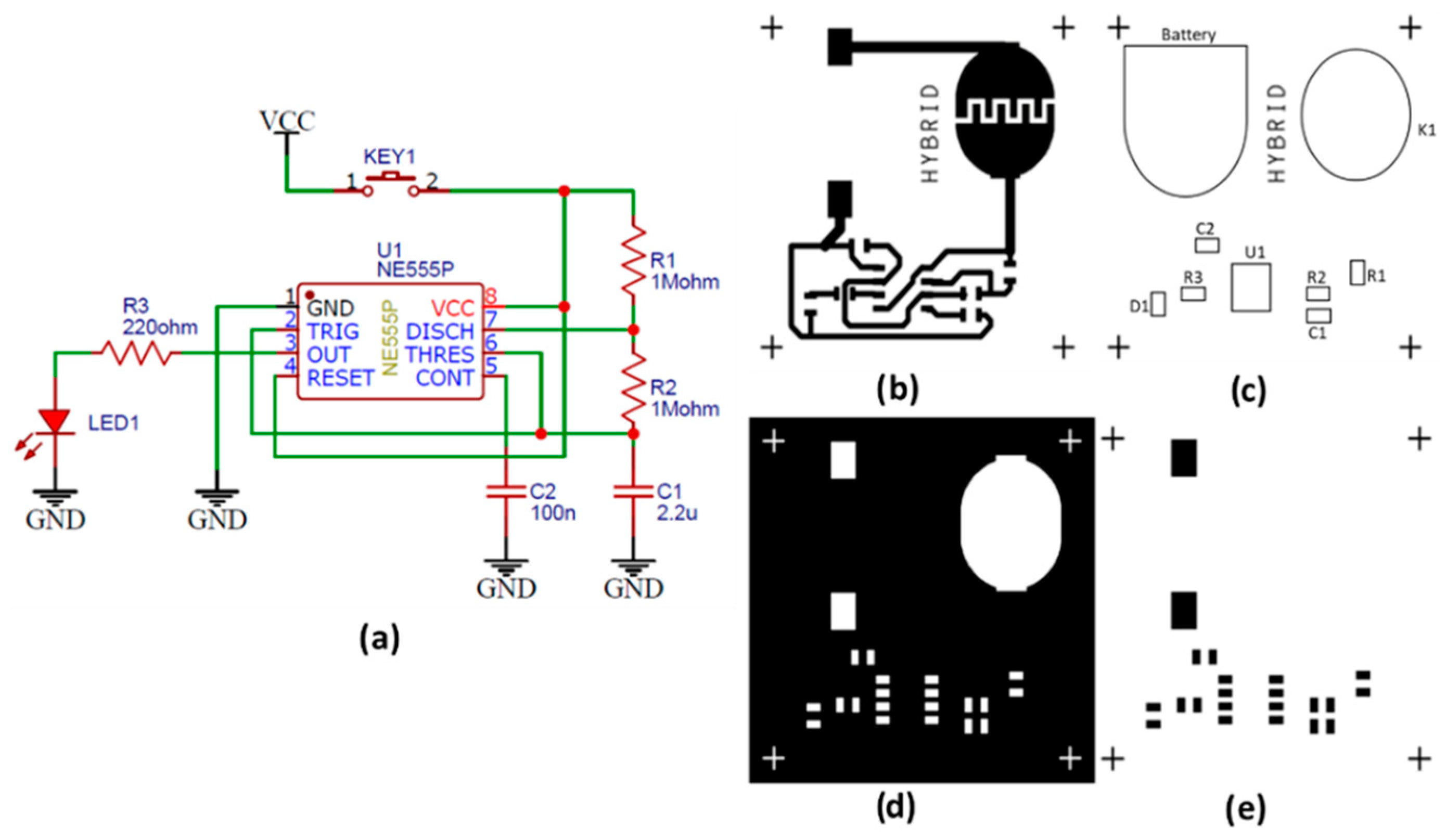
2.3. Soldering Methods and Test Pattern: Low-Temperature Solders
2.3.1. Soldering Profiles
2.3.2. Soldering Joint Resistance
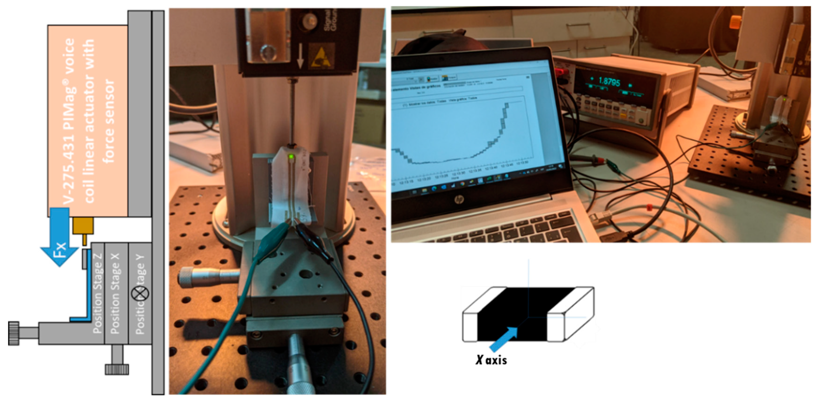
2.3.3. Shear Test
2.3.4. Optical Microscopy
3. Results and Discussion
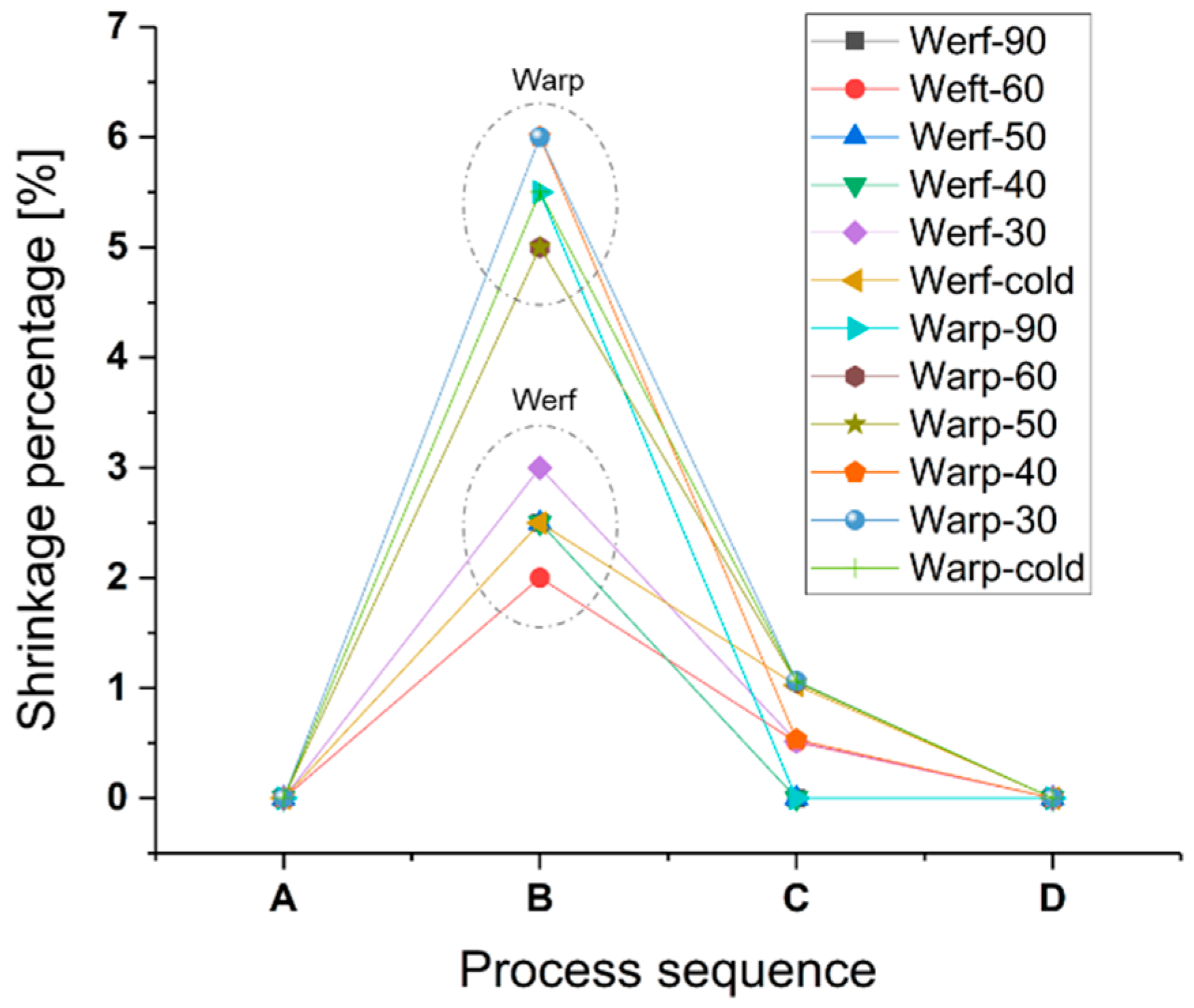
3.1. Shrinkage Percentage
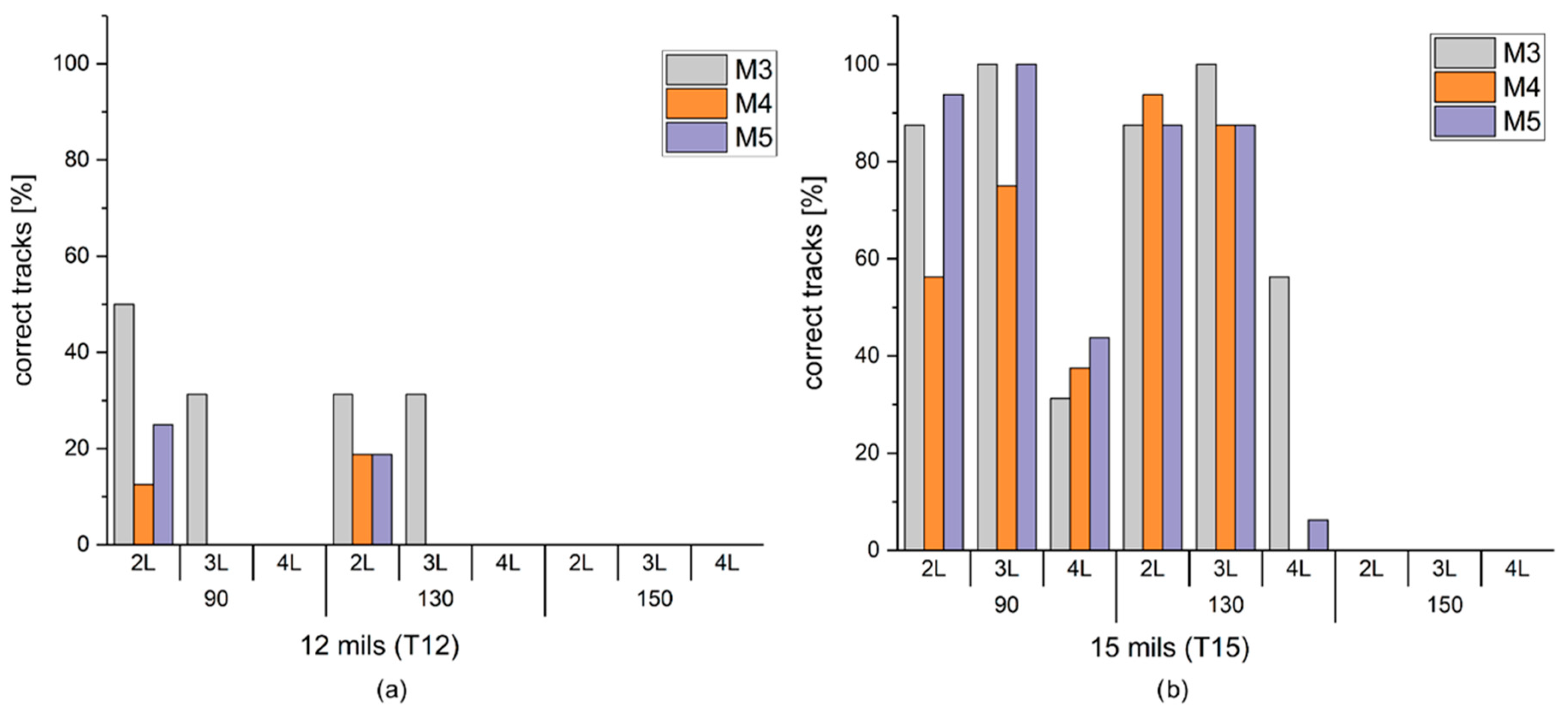
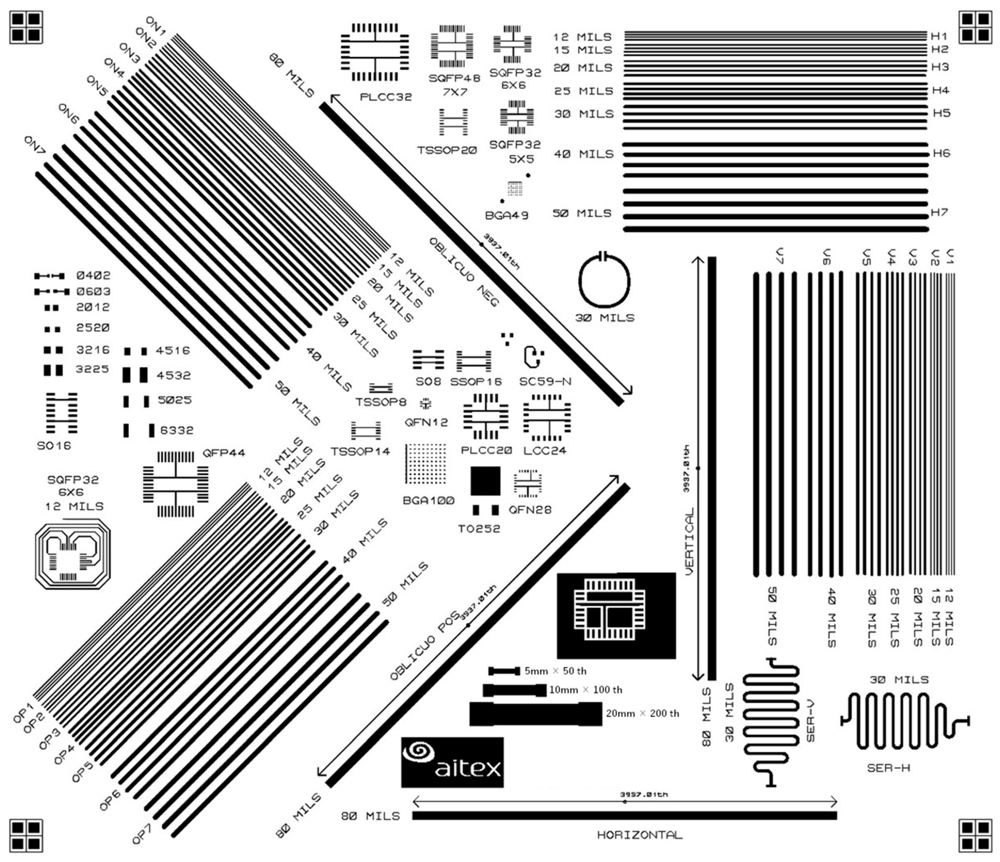
3.2. Minimum Design Parameters
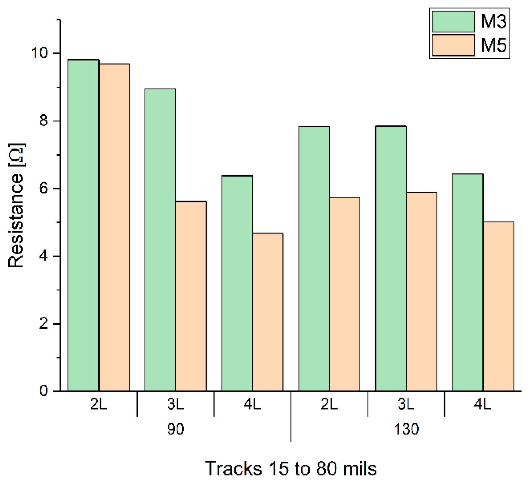
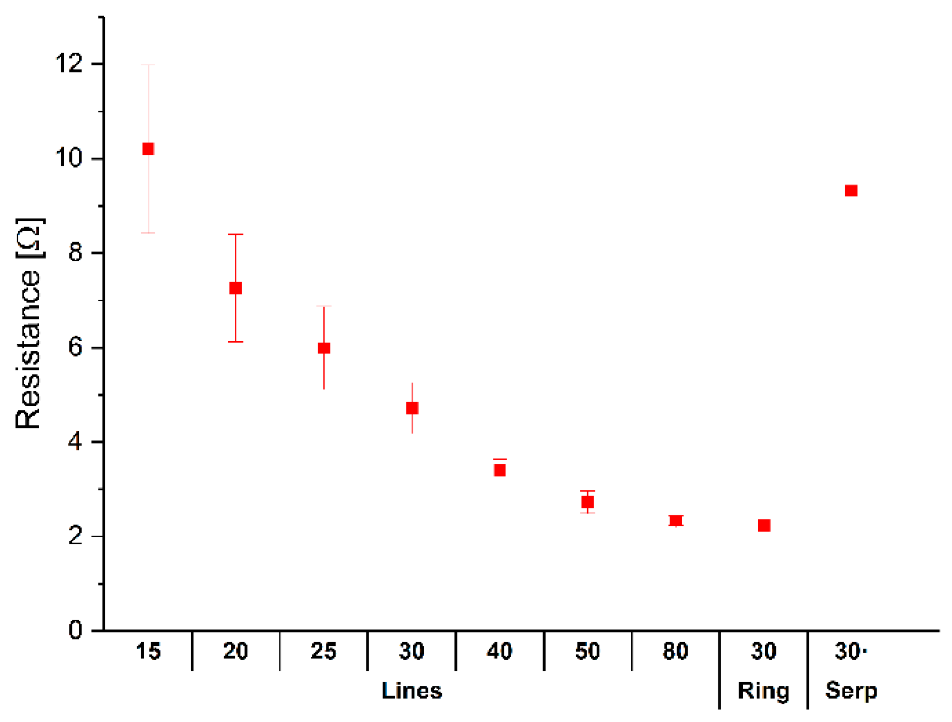
3.2.1. Electrical Parameters
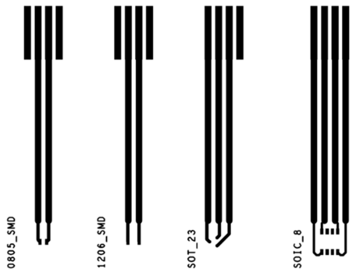
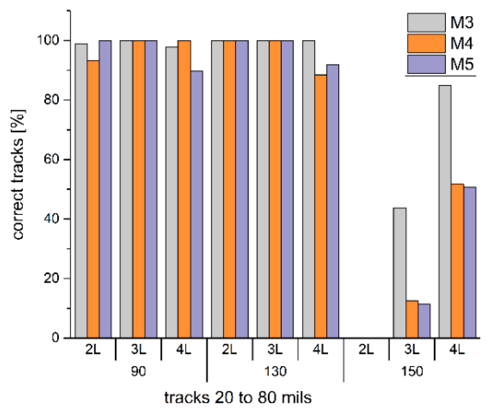
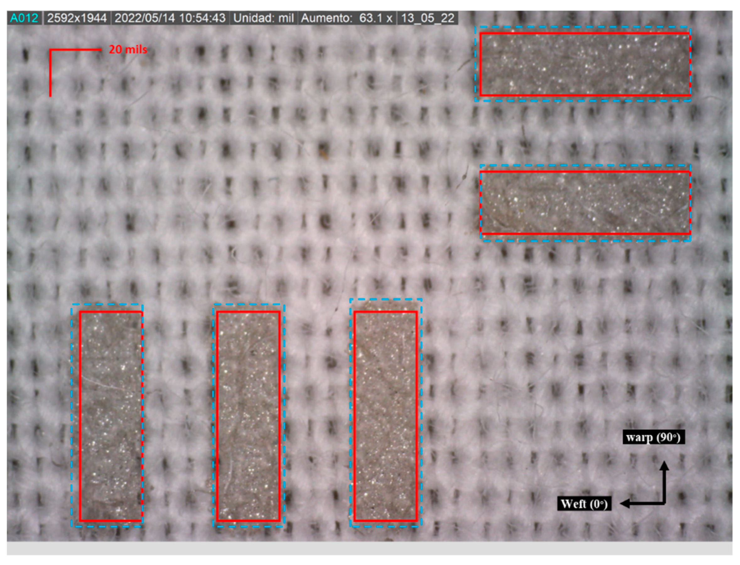
3.2.2. Dimensional Parameters
3.3. Soldering Test
3.3.1. Soldering Profiles
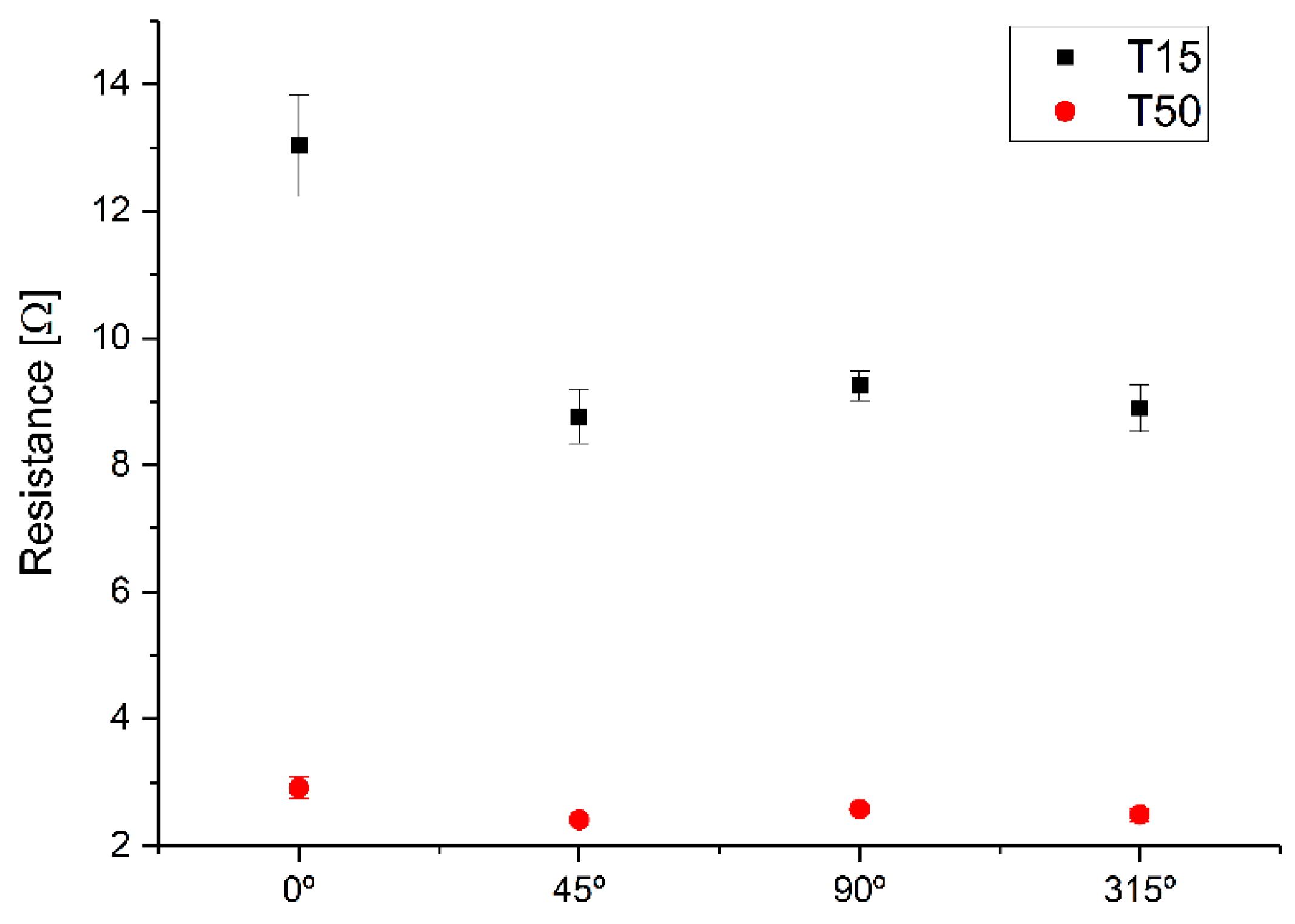
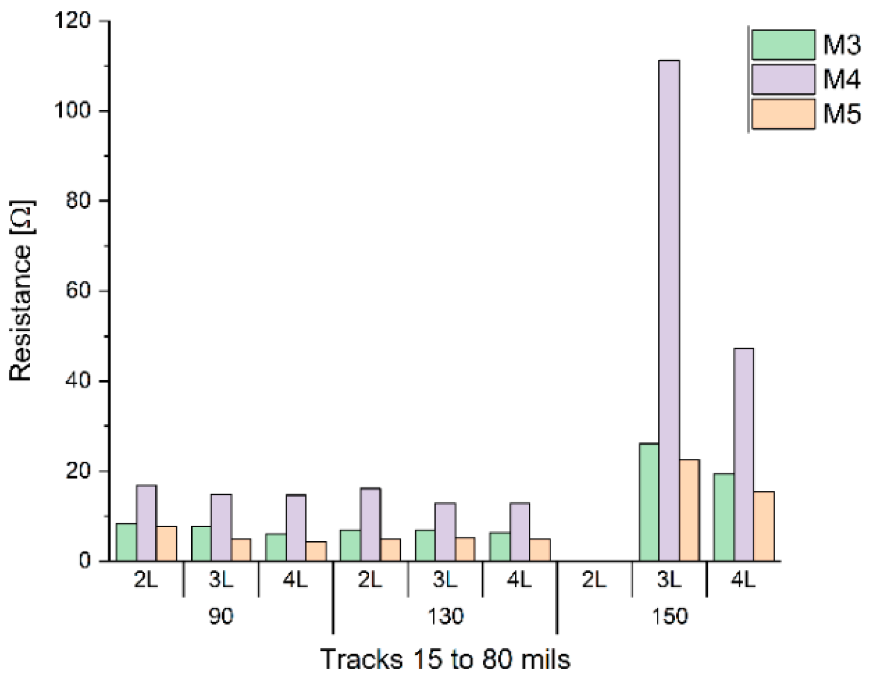
3.3.2. Soldering Joint Resistance
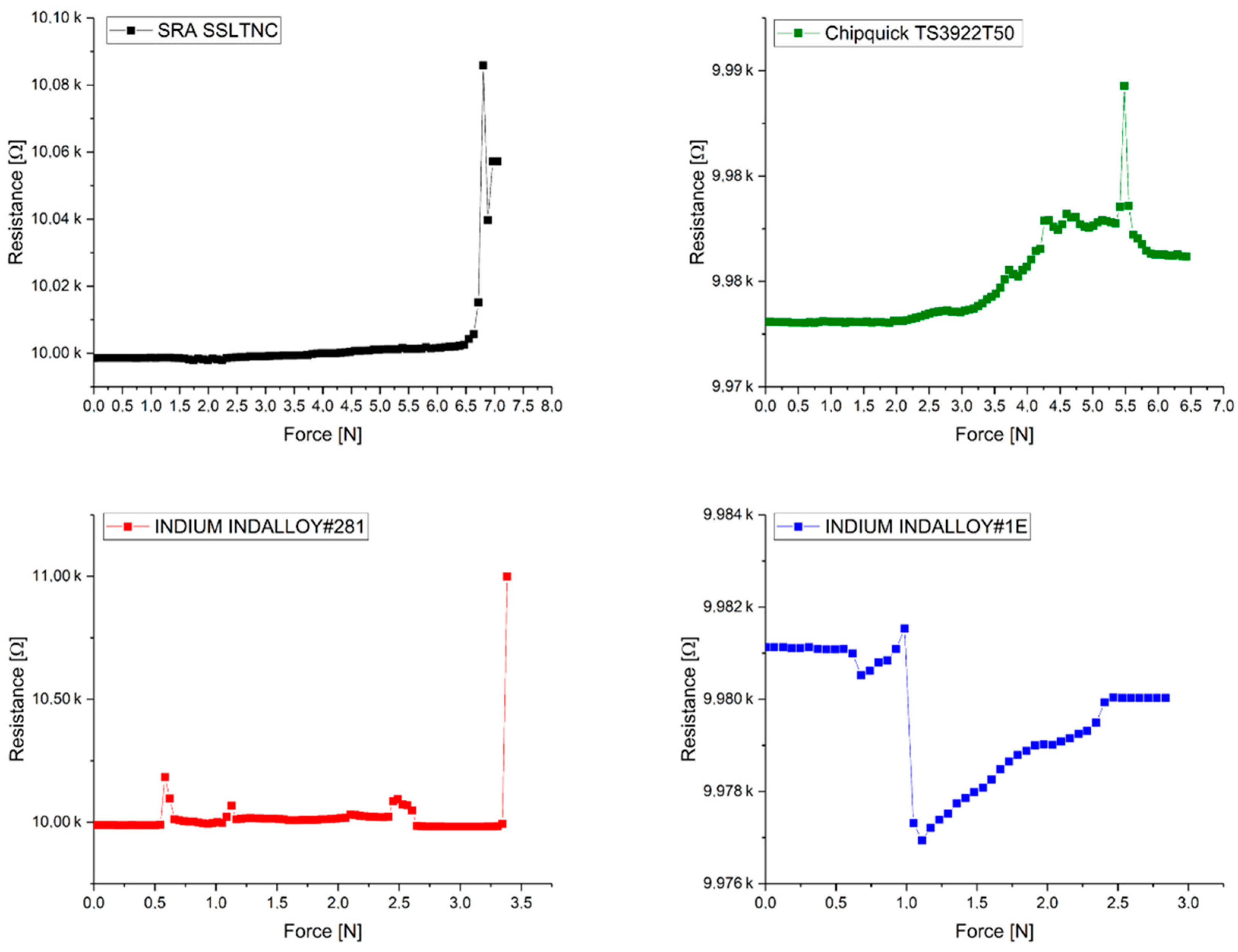
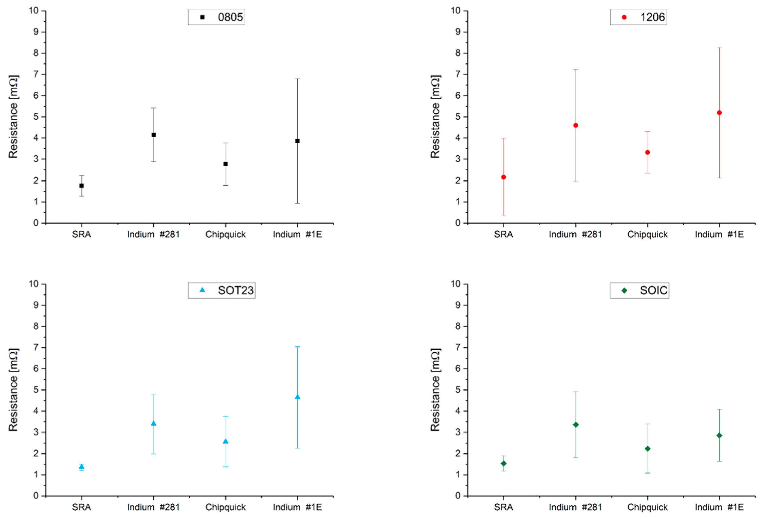
3.3.3. Shear Test
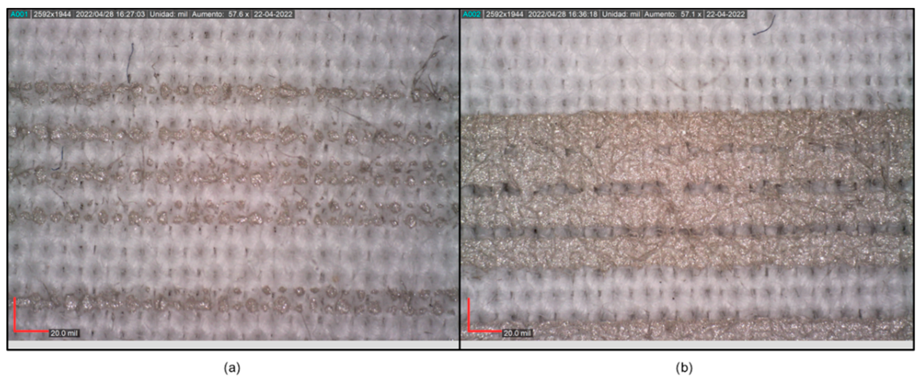
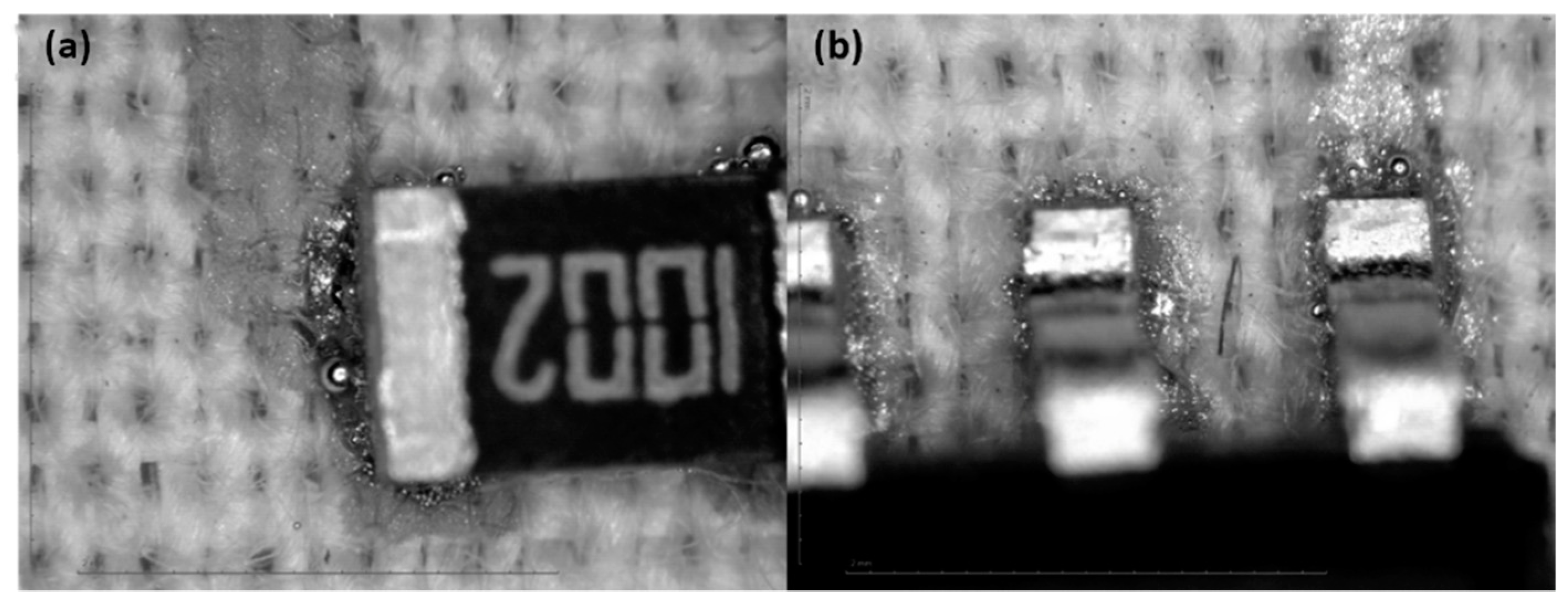
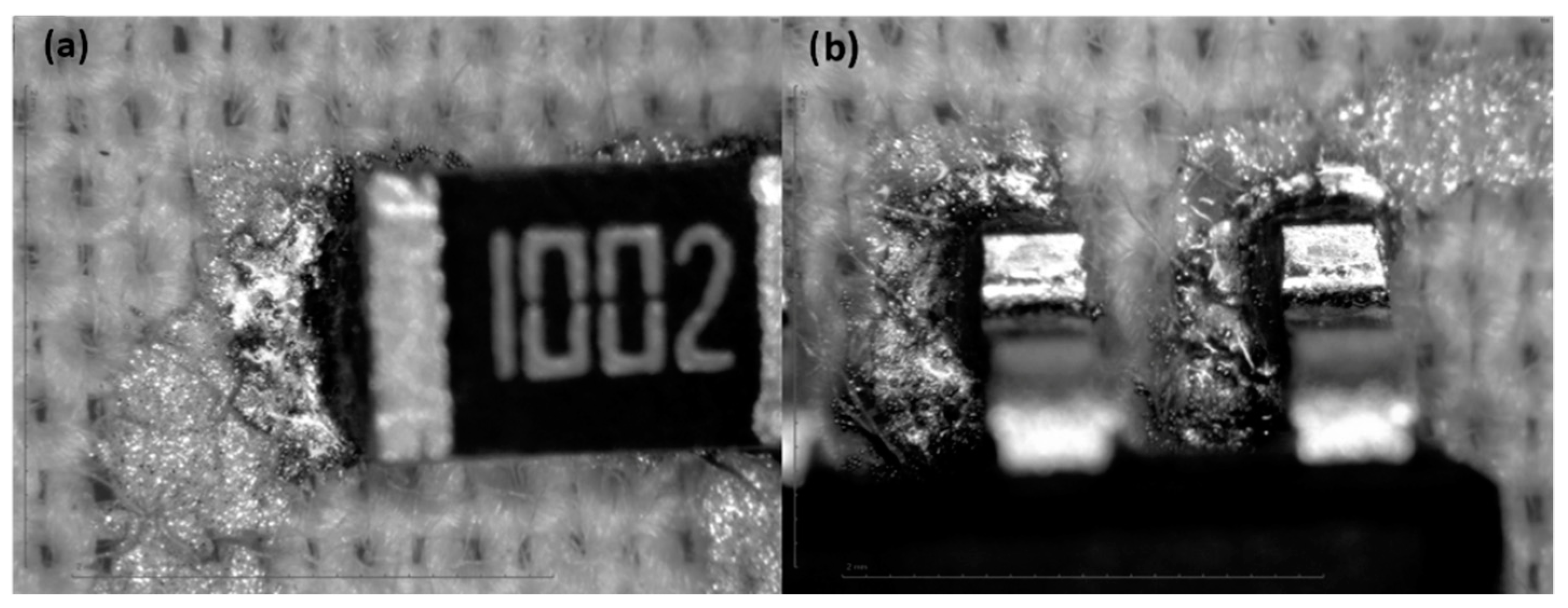
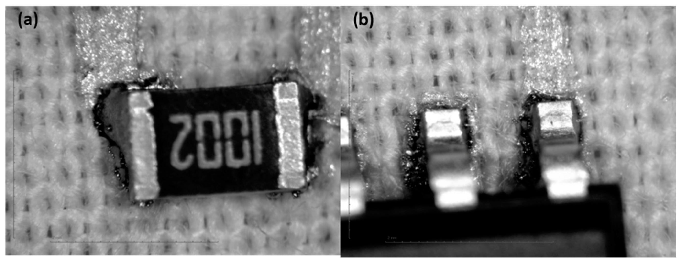
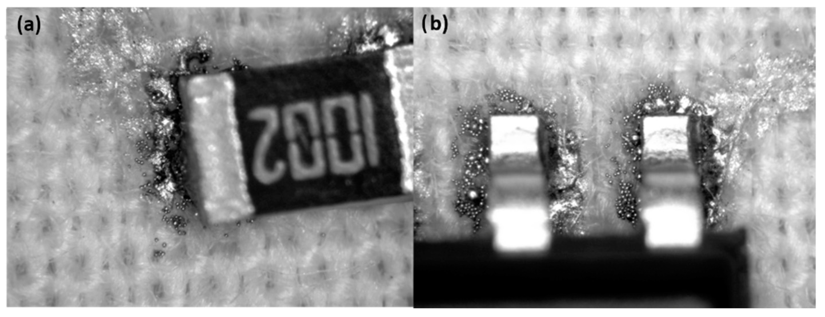
3.3.4. Optical Characterization
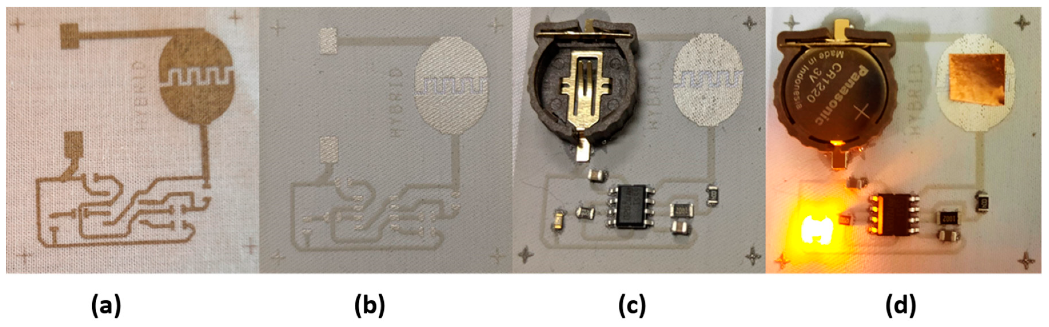
3.3.5. Circuit on Textile
4. Conclusions
Author Contributions
Funding
Institutional Review Board Statement
Informed Consent Statement
Data Availability Statement
Conflicts of Interest
Appendix A


| Alloys | Liquidus | Solidus | Indium Indalloy | Chipquick | Nevo | Alpha | SRA | Superior Flux | Gemma Europe | AIM |
|---|---|---|---|---|---|---|---|---|---|---|
| 48Sn/52In | 118 | 118 | 1E | |||||||
| 50In/50Sn | 125 | 118 | 1 | |||||||
| 52Sn/48In | 131 | 118 | 71 | SmdIn52Sn48 | ||||||
| 42Sn/58Bi | 138 | 138 | 281 | Pf602-p-t3-500 | Sb58-cosmo-nh-t4 | |||||
| 42Sn/57.6Bi/0.4Ag | 139 | 138 | Ts391lt50 | Cvp-520 | ||||||
| 42Sn/57Bi/1Ag | 140 | 139 | 282 | Smdswltlfp31 | Ssltnc | 59-193-90 | Nc273lt | |||
| 42.6Sn/57Bi/0.4Ag | 141 | 139 | Sb6-hlgq-msd | |||||||
| 97In/3Ag | 143 | 143 | 290 | SmdIn97Ag3 | ||||||
| 42In/58Sn | 145 | 118 | 87 | |||||||
| 95In/5Bi | 150 | 125 | 203 | |||||||
| 99.3In/0.7Ga | 150 | 150 | 88 | |||||||
| 90In/10Sn | 151 | 143 | 225 | |||||||
| 99.4In/0.6Ga | 152 | 152 | 90 | |||||||
| 99.6In/0.4Ga | 153 | 153 | 91 | |||||||
| 99.5In/0.5Ga | 154 | 154 | 92 | |||||||
| 100In | 157 | 157 | 4 | SmdIn | ||||||
| 86.5Sn/5.5Zn/4.5In/3.5Bi | 186 | 174 | 231 | |||||||
| 20In/77.2Sn/2.8Ag | 187 | 175 | 227 | |||||||
| 8.8In/83.6Sn7.6Zn | 187 | 181 | 226 |
| PET1500 90/230-48PW | PET1500 130/330-34PW | PET1500 150/380-34PW | |
|---|---|---|---|
| Mesh count [cm−1] | 90 | 130 | 150 |
| Thread diameter Nominal [µm] | 48 | 34 | 34 |
| Mesh opening [µm] | 55 | 40 | 23 |
| Open area [%] | 25 | 27 | 12 |
| Mesh thickness (woven) [µm] | 76 | 53 | 54 |
| Device | Land Pattern | X (TW) | Y (TW) | Gap1 (PP) | Pitch1 | Gap2 (PP) | Pitch2 | D (PP) | Z (PP) |
|---|---|---|---|---|---|---|---|---|---|
| 08052012 * |  | 60 | 50 | 25 | 126 | - | - | - | - |
| 12063216 * |  | 89 | 40 | 72 | 112 | - | - | - | - |
| SOIC8 | 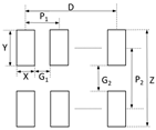 | 24 | 87 | 26 | 50 | 118 | 205 | 150 | 291 |
| SOT23 |  | 39 | 55 | 35 | 74 | 32 | 87 | 39 | 55 |
References
- Li, Z.; Zhang, R.; Moon, K.-S.; Liu, Y.; Hansen, K.; Le, T.; Wong, C.P. Highly Conductive, Flexible, Polyurethane-Based Adhesives for Flexible and Printed Electronics. Adv. Funct. Mater. 2013, 23, 1459–1465. [Google Scholar] [CrossRef]
- Hyun, W.J.; Secor, E.B.; Hersam, M.C.; Frisbie, C.D.; Francis, L.F. High-Resolution Patterning of Graphene by Screen Printing with a Silicon Stencil for Highly Flexible Printed Electronics. Adv. Mater. 2015, 27, 109–115. [Google Scholar] [CrossRef]
- Paul, G.; Torah, R.; Yang, K.; Beeby, S.; Tudor, J. An investigation into the durability of screen-printed conductive tracks on textiles. Meas. Sci. Technol. 2014, 25, 025006. [Google Scholar] [CrossRef]
- Luo, C.; Gil, I.; Fernández-García, R. Wearable Textile UHF-RFID Sensors: A Systematic Review. Materials 2020, 13, 3292. [Google Scholar] [CrossRef] [PubMed]
- Carey, T.; Cacovich, S.; Divitini, G.; Ren, J.; Mansouri, A.; Kim, J.M.; Wang, C.; Ducati, C.; Sordan, R.; Torrisi, F. Fully inkjet-printed two-dimensional material field-effect heterojunctions for wearable and textile electronics. Nat. Commun. 2017, 8, 1202. [Google Scholar] [CrossRef] [PubMed] [Green Version]
- Lee, S.; Kim, B.; Roh, T.; Hong, S.; Yoo, H.-J. Arm-band type textile-MP3 player with multi-layer Planar Fashionable Circuit Board (P-FCB) techniques. In Proceedings of the International Symposium on Wearable Computers, Seoul, Korea, 10–13 October 2010. [Google Scholar]
- Wang, L.B.; See, K.Y.; Zhang, J.W.; Salam, B.; Lu, A.C.W. Ultrathin and Flexible Screen-Printed Metasurfaces for EMI Shielding Applications. IEEE Trans. Electromagn. Compat. 2011, 53, 700–705. [Google Scholar] [CrossRef]
- Chang, J.S.; Facchetti, A.F.; Reuss, R. A Circuits and Systems Perspective of Organic/Printed Electronics: Review, Challenges, and Contemporary and Emerging Design Approaches. IEEE J. Emerg. Sel. Top. Circuits Syst. 2017, 7, 7–26. [Google Scholar] [CrossRef]
- Brooke, R.; Wijeratne, K.; Hübscher, K.; Belaineh, D.; Ersman, P.A. Combining Vapor Phase Polymerization and Screen Printing for Printed Electronics on Flexible Substrates. Adv. Mater. Technol. 2022, 7, 2101665. [Google Scholar] [CrossRef]
- Janczak, D.; Zych, M.; Raczyński, T.; Dybowska-Sarapuk, Ł.; Pepłowski, A.; Krzemiński, J.; Sosna-Głębska, A.; Znajdek, K.; Sibiński, M.; Jakubowska, M. Stretchable and Washable Electroluminescent Display Screen-Printed on Textile. Nanomaterials 2019, 9, 1276. [Google Scholar] [CrossRef] [Green Version]
- Kang, J.S.; Kim, H.S.; Ryu, J.; Hahn, H.T.; Jang, S.; Joung, J.W. Inkjet printed electronics using copper nanoparticle ink. J. Mater. Sci. Mater. Electron. 2010, 21, 1213–1220. [Google Scholar] [CrossRef] [Green Version]
- Jain, K.; Klosner, M.; Zemel, M.; Raghunandan, S. Flexible Electronics and Displays: High-Resolution, Roll-to-Roll, Projection Lithography and Photoablation Processing Technologies for High-Throughput Production. Proc. IEEE 2005, 93, 1500–1510. [Google Scholar] [CrossRef]
- Mariappan, D.D.; Kim, S.; Hart, A.J. A precision desktop plate-to-roll apparatus for development of advanced flexographic printing processes. Precis. Eng. 2020, 66, 392–400. [Google Scholar] [CrossRef]
- Morgan, M.L.; Curtis, D.; Deganello, D. Control of morphological and electrical properties of flexographic printed electronics through tailored ink rheology. Org. Electron. 2019, 73, 212–218. [Google Scholar] [CrossRef]
- Sung, D.; De La Fuente Vornbrock, A.; Subramanian, V. Scaling and Optimization of Gravure-Printed Silver Nanoparticle Lines for Printed Electronics. IEEE Trans. Components Packag. Technol. 2010, 33, 105–114. [Google Scholar] [CrossRef]
- Grau, G.; Cen, J.; Kang, H.; Kitsomboonloha, R.; Scheideler, W.J.; Subramanian, V. Gravure-printed electronics: Recent progress in tooling development, understanding of printing physics, and realization of printed devices. Flex. Print. Electron. 2016, 1, 023002. [Google Scholar] [CrossRef]
- Kusaka, Y.; Fukuda, N.; Ushijima, H. Recent advances in reverse offset printing: An emerging process for high-resolution printed electronics. Jpn. J. Appl. Phys. 2020, 59, SG0802. [Google Scholar] [CrossRef]
- Mo, L.; Guo, Z.; Yang, L.; Zhang, Q.; Fang, Y.; Xin, Z.; Chen, Z.; Hu, K.; Han, L.; Li, L. Silver Nanoparticles Based Ink with Moderate Sintering in Flexible and Printed Electronics. Int. J. Mol. Sci. 2019, 20, 2124. [Google Scholar] [CrossRef] [Green Version]
- Wu, Y.; Li, Y.; Ong, B.S. A Simple and Efficient Approach to a Printable Silver Conductor for Printed Electronics. J. Am. Chem. Soc. 2007, 129, 1862–1863. [Google Scholar] [CrossRef]
- Reiser, B.; González-García, L.; Kanelidis, I.; Maurer, J.H.M.; Kraus, T. Gold nanorods with conjugated polymer ligands: Sintering-free conductive inks for printed electronics. Chem. Sci. 2016, 7, 4190–4196. [Google Scholar] [CrossRef] [Green Version]
- Bacalzo, N.P.; Go, L.P.; Querebillo, C.J.; Hildebrandt, P.; Limpoco, F.T.; Enriquez, E.P. Controlled Microwave-Hydrolyzed Starch as a Stabilizer for Green Formulation of Aqueous Gold Nanoparticle Ink for Flexible Printed Electronics. ACS Appl. Nano Mater. 2018, 1, 1247–1256. [Google Scholar] [CrossRef]
- Patil, S.A.; Ryu, C.-H.; Kim, H.-S. Synthesis and Characterization of Copper Nanoparticles (Cu-Nps) using Rongalite as Reducing Agent and Photonic Sintering of Cu-Nps Ink for Printed Electronics. Int. J. Precis. Eng. Manuf. Technol. 2018, 5, 239–245. [Google Scholar] [CrossRef]
- Magdassi, S.; Grouchko, M.; Kamyshny, A. Copper Nanoparticles for Printed Electronics: Routes towards Achieving Oxidation Stability. Materials 2010, 3, 4626–4638. [Google Scholar] [CrossRef] [PubMed] [Green Version]
- Altay, B.N.; Jourdan, J.S.; Turkani, V.S.; Dietsch, H.; Maddipatla, D.; Pekarovicova, A.; Fleming, P.D.; Atashbar, M.Z. Impact of Substrate and Process on the Electrical Performance of Screen-Printed Nickel Electrodes: Fundamental Mechanism of Ink Film Roughness. ACS Appl. Energy Mater. 2018, 1, 7164–7173. [Google Scholar] [CrossRef]
- Park, S.-H.; Kim, H.-S. Flash light sintering of nickel nanoparticles for printed electronics. Thin Solid Films 2014, 550, 575–581. [Google Scholar] [CrossRef]
- Busato, S.; Belloli, A.; Ermanni, P. Inkjet printing of palladium catalyst patterns on polyimide film for electroless copper plating. Sens. Actuators B Chem. 2007, 123, 840–846. [Google Scholar] [CrossRef]
- Wang, X.; Liu, J. Recent Advancements in Liquid Metal Flexible Printed Electronics: Properties, Technologies, and Applications. Micromachines 2016, 7, 206. [Google Scholar] [CrossRef] [PubMed]
- Lall, P.; Narangaparambil, J.; Leever, B.; Miller, S. Effect of Sintering Temperature on the Fatigue Life of Additively Printed Electronics during Cyclic Bending. In Proceedings of the 2019 18th IEEE Intersociety Conference on Thermal and Thermomechanical Phenomena in Electronic Systems (ITherm), Las Vegas, NV, USA, 28–31 May 2019; Volume 2019. [Google Scholar]
- Linz, T.; Kallmayer, C.; Aschenbrenner, R.; Reichl, H. Embroidering electrical interconnects with conductive yarn for the integration of flexible electronic modules into fabric. In Proceedings of the Ninth IEEE International Symposium on Wearable Computers (ISWC’05), Osaka, Japan, 18–21 October 2005; pp. 86–89. [Google Scholar] [CrossRef]
- Vervust, T.; Buyle, G.; Bossuyt, F.; Vanfleteren, J. Integration of stretchable and washable electronic modules for smart textile applications. J. Text. Inst. 2012, 103, 1127–1138. [Google Scholar] [CrossRef]
- Tao, X.; Koncar, V.; Huang, T.-H.; Shen, C.-L.; Ko, Y.-C.; Jou, G.-T. How to Make Reliable, Washable, and Wearable Textronic Devices. Sensors 2017, 17, 673. [Google Scholar] [CrossRef] [PubMed] [Green Version]
- Ferri, J.; Llopis, R.L.; Moreno, J.; Lidón-Roger, J.V.; Garcia-Breijo, E. An investigation into the fabrication parameters of screen-printed capacitive sensors on e-textiles. Text. Res. J. 2020, 90, 1749–1769. [Google Scholar] [CrossRef]
- Yang, G.; Xie, L.; Mäntysalo, M.; Chen, J.; Tenhunen, H.; Zheng, L.-R. Bio-Patch Design and Implementation Based on a Low-Power System-on-Chip and Paper-Based Inkjet Printing Technology. IEEE Trans. Inf. Technol. Biomed. 2012, 16, 1043–1050. [Google Scholar] [CrossRef] [PubMed]
- Locher, I.; Troster, G. Fundamental Building Blocks for Circuits on Textiles. IEEE Trans. Adv. Packag. 2007, 30, 541–550. [Google Scholar] [CrossRef]
- Xie, L.; Yang, G.; Mäntysalo, M.; Xu, L.-L.; Jonsson, F.; Zheng, L.-R. Heterogeneous Integration of Bio-Sensing System-on-Chip and Printed Electronics. IEEE J. Emerg. Sel. Top. Circuits Syst. 2012, 2, 672–682. [Google Scholar] [CrossRef]
- Koshi, T.; Nomura, K.-I.; Yoshida, M. Electronic Component Mounting for Durable E-Textiles: Direct Soldering of Components onto Textile-Based Deeply Permeated Conductive Patterns. Micromachines 2020, 11, 209. [Google Scholar] [CrossRef] [PubMed] [Green Version]
- Agcayazi, T.; Chatterjee, K.; Bozkurt, A.; Ghosh, T.K. Flexible Interconnects for Electronic Textiles. Adv. Mater. Technol. 2018, 3, 1–32. [Google Scholar] [CrossRef]
- Stanley, J.; Hunt, J.A.; Kunovski, P.; Wei, Y. A review of connectors and joining technologies for electronic textiles. Eng. Rep. 2021, 4, e12491. [Google Scholar] [CrossRef]
- Palavesam, N.; Marin, S.; Hemmetzberger, D.; Landesberger, C.; Bock, K.; Kutter, C. Roll-to-roll processing of film substrates for hybrid integrated flexible electronics. Flex. Print. Electron. 2018, 3, 014002. [Google Scholar] [CrossRef]
- Wang, F.; Chen, H.; Huang, Y.; Liu, L.; Zhang, Z. Recent progress on the development of Sn–Bi based low-temperature Pb-free solders. J. Mater. Sci. Mater. Electron. 2019, 30, 3222–3243. [Google Scholar] [CrossRef]
- Yang, K.; Torah, R.; Wei, Y.; Beeby, S.; Tudor, J. Waterproof and durable screen printed silver conductive tracks on textiles. Text. Res. J. 2013, 83, 2023–2031. [Google Scholar] [CrossRef]
- Cook, J. Handbook of Textile Fibres: Man-Made Fibres; Woodhead Publishing Limited: Sawston, UK, 1984. [Google Scholar]
- Choudhury, A.K.R. Flame Retardants for Textile Materials. In Flame Retardants for Textile Materials; CRC Press: Boca Raton, FL, USA, 2020. [Google Scholar] [CrossRef]
- Perera, H.A.A.E.; Lanarolle, W.D.G. Thermal behaviour of heat treated polyester knitted fabrics. Res. J. Text. Appar. 2020, 24, 305–319. [Google Scholar] [CrossRef]
- Xia, Z.; Yao, C.; Zhou, J.; Ye, W.; Xu, W. Comparative study of cotton, ramie and wool fiber bundles’ thermal and dynamic mechanical thermal properties. Text. Res. J. 2015, 86, 856–867. [Google Scholar] [CrossRef]
- Tu, K.; Zeng, K. Tin–lead (SnPb) solder reaction in flip chip technology. Mater. Sci. Eng. R Rep. 2001, 34, 1–58. [Google Scholar] [CrossRef]
- Zhang, L.; Tu, K. Structure and properties of lead-free solders bearing micro and nano particles. Mater. Sci. Eng. R Rep. 2014, 82, 1–32. [Google Scholar] [CrossRef]
- Silva, B.; Xavier, M.G.; Garcia, A.; Spinelli, J.E. Cu and Ag additions affecting the solidification microstructure and tensile properties of Sn-Bi lead-free solder alloys. Mater. Sci. Eng. A 2017, 705, 325–334. [Google Scholar] [CrossRef]
- Xu, K.-K.; Zhang, L.; Gao, L.-L.; Jiang, N.; Zhang, L.; Zhong, S.-J. Review of microstructure and properties of low temperature lead-free solder in electronic packaging. Sci. Technol. Adv. Mater. 2020, 21, 689–711. [Google Scholar] [CrossRef] [PubMed]
- Kotadia, H.R.; Howes, P.D.; Mannan, S.H. A review: On the development of low melting temperature Pb-free solders. Microelectron. Reliab. 2014, 54, 1253–1273. [Google Scholar] [CrossRef]
- Raj, R.; Shrivastava, P.; Jindal, N.; Alam, S.N.; Naithani, N.; Padhy, M.; Phani, A.S.D.; Ramana, T.V.V.; Abbas, M.M. Development and Characterization of Eutectic Sn-Zn, Sn-Ag, Sn-Bi and Sn-Cu Solder Alloys. Int. J. Mater. Res. 2019, 110. [Google Scholar] [CrossRef]
- Kang, H.; Rajendran, S.H.; Jung, J.P. Low Melting Temperature Sn-Bi Solder: Effect of Alloying and Nanoparticle Addition on the Microstructural, Thermal, Interfacial Bonding, and Mechanical Characteristics. Metals 2021, 11, 364. [Google Scholar] [CrossRef]
- Jiang, N.; Zhang, L.; Gao, L.-L.; Song, X.-G.; He, P. Recent advances on SnBi low-temperature solder for electronic interconnections. J. Mater. Sci. Mater. Electron. 2021, 32, 22731–22759. [Google Scholar] [CrossRef]
- Gonzalez, M.; Vandevelde, B.; Christiaens, W.; Hsu, Y.-Y.; Iker, F.; Bossuyt, F.; Vanfleteren, J.; van der Sluis, O.; Timmermans, P. Design and implementation of flexible and stretchable systems. Microelectron. Reliab. 2011, 51, 1069–1076. [Google Scholar] [CrossRef]


| Fabric | Picture | Weft Material | Warp Material | Ligament | |
|---|---|---|---|---|---|
| 100% Waterproof Cotton |  | Cotton | Cotton | Taffeta |  |
| Fabric | Weft Density (Thread/cm) | Warp Density (Thread/cm) | Fabric Density (Thread/cm2) | Wire Weft Diameter (µm) | Wire Warp Diameter (µm) | Thickness (µm) | Grammage (g/m2) |
|---|---|---|---|---|---|---|---|
| 100% Waterproof Cotton | 32 | 44 | 76 | 160 | 160 | 130 ± 5 | 115 ± 6 |
| SCAG-003 | SCAG-004 | SCAG-005 | |
|---|---|---|---|
| Sheet Resistivity (Ω/sq@25 µm) | <0.05 | <0.06 | <0.02 |
| Solids (%) | 70–81.5 | 70–80 | 75–80 |
| Density (g/cm3) | 3.16 | 3.1 | 3.12 |
| Viscosity (Pas) | 14.3–14.8 @200 s−1 | 39.9 @10 s−1 | 40–50 @10 s−1 |
| Screens polyester (Threads/cm). µm | 130.30 | 650.14 | 130.30 |
| Curing Box oven | 130 °C—20–30 min | 130 °C—20–30 min | 160 °C—10 min |
| Properties | Silver/Silver-Copper Very high definition | Silver/Silver-Copper Very high definition | Silver High definition High Conductivity |
| Alloys | Liquidus | Solidus | Mesh Size | Metal Load | Peak Temperature Time Max. | |
|---|---|---|---|---|---|---|
| Indium Indalloy #1E | 48Sn/52In | 118 | 118 | T3 | 89% | 143–163 °C <60 s |
| Indium Indalloy #281 | 42Sn/58Bi | 138 | 138 | T3 | 84% | 163–183 °C <60 s |
| Chipquick TS3911T50 | 42Sn/57.6Bi/0.4Ag | 139 | 138 | T4 | 90% | 165 °C <40 s |
| SRA SSLTNC | 42Sn/57Bi/1Ag | 140 | 139 | T3 | 87–90% | 165 °C <45 s |
| T15 | T20 | T25 | T30 | T40 | T50 | T80 | |
|---|---|---|---|---|---|---|---|
| 0° | 19.02 ± 1.05 | 21.54 ± 1.54 | 24.23 ± 2.54 | 31.36 ± 1.56 | 42.46 ± 1.49 | 51.00 ± 0.97 | 79.07 ± 4.31 |
| 45° | 16.19 ± 3.66 | 20.08 ± 1.66 | 25.13 ± 1.74 | 29.63 ± 3.00 | 40.33 ± 1.67 | 48.24 ± 2.90 | 82.19 ± 3.46 |
| 90° | 18.05 ± 1.95 | 21.54 ± 1.40 | 24.61 ± 1.01 | 30.98 ± 1.78 | 42.70 ± 1.51 | 51.32 ± 1.38 | 84.90 ± 2.45 |
| 315° | 17.20 ± 2.10 | 21.38 ± 1.00 | 24.21 ± 1.92 | 31.60 ± 2.12 | 42.38 ± 2.44 | 51.81 ± 2.66 | 82.82 ± 2.75 |
| 0805 | 1206 | SOT23 | |
|---|---|---|---|
| SRA SSLTNC | 7.0 | 4.6 | 10.5 |
| Chipquick TS3922T50 | 6.3 | 4.6 | 9.0 |
| Indium Indalloy#281 | 3.7 | 4.2 | 6.9 |
| Indium Indalloy#1E | 2.9 | 2.9 | 6.9 |
Publisher’s Note: MDPI stays neutral with regard to jurisdictional claims in published maps and institutional affiliations. |
© 2022 by the authors. Licensee MDPI, Basel, Switzerland. This article is an open access article distributed under the terms and conditions of the Creative Commons Attribution (CC BY) license (https://creativecommons.org/licenses/by/4.0/).
Share and Cite
Silvestre, R.; Llinares Llopis, R.; Contat Rodrigo, L.; Serrano Martínez, V.; Ferri, J.; Garcia-Breijo, E. Low-Temperature Soldering of Surface Mount Devices on Screen-Printed Silver Tracks on Fabrics for Flexible Textile Hybrid Electronics. Sensors 2022, 22, 5766. https://doi.org/10.3390/s22155766
Silvestre R, Llinares Llopis R, Contat Rodrigo L, Serrano Martínez V, Ferri J, Garcia-Breijo E. Low-Temperature Soldering of Surface Mount Devices on Screen-Printed Silver Tracks on Fabrics for Flexible Textile Hybrid Electronics. Sensors. 2022; 22(15):5766. https://doi.org/10.3390/s22155766
Chicago/Turabian StyleSilvestre, Rocío, Raúl Llinares Llopis, Laura Contat Rodrigo, Víctor Serrano Martínez, Josué Ferri, and Eduardo Garcia-Breijo. 2022. "Low-Temperature Soldering of Surface Mount Devices on Screen-Printed Silver Tracks on Fabrics for Flexible Textile Hybrid Electronics" Sensors 22, no. 15: 5766. https://doi.org/10.3390/s22155766
APA StyleSilvestre, R., Llinares Llopis, R., Contat Rodrigo, L., Serrano Martínez, V., Ferri, J., & Garcia-Breijo, E. (2022). Low-Temperature Soldering of Surface Mount Devices on Screen-Printed Silver Tracks on Fabrics for Flexible Textile Hybrid Electronics. Sensors, 22(15), 5766. https://doi.org/10.3390/s22155766