Article

Single VDGA-Based Mixed-Mode Universal Filter and Dual-Mode Quadrature Oscillator

by
Natchanai Roongmuanpha
,
Worapong Tangsrirat
* and
Tattaya Pukkalanun
School of Engineering, King Mongkut’s Institute of Technology Ladkrabang (KMITL), Bangkok 10520, Thailand
*
Author to whom correspondence should be addressed.
Sensors 2022, 22(14), 5303; https://doi.org/10.3390/s22145303
Submission received: 2 June 2022 / Revised: 6 July 2022 / Accepted: 8 July 2022 / Published: 15 July 2022
(This article belongs to the Section Electronic Sensors)

Abstract

:
This article presents the circuit designs for a mixed-mode universal biquadratic filter and a dual-mode quadrature oscillator, both of which use a single voltage differencing gain amplifier (VDGA), one resistor, and two capacitors. The proposed circuit has the following performance characteristics: (i) simultaneous implementation of standard biquadratic filter functions with three inputs and two outputs in all four possible modes, namely, voltage-mode (VM), current-mode (CM), trans-admittance-mode (TAM), and trans-impedance-mode (TIM); (ii) electronic adjustment of the natural angular frequency and independently single-resistance controllable high-quality factor; (iii) performing a dual-mode quadrature oscillator with simultaneous voltage and current output responses; (iv) orthogonal resistive and/or electronic control of the oscillation condition and frequency; (v) employing all grounded passive components in the quadrature oscillator function; and (vi) simpler topology due to the use of a single VDGA. VDGA non-idealities and parasitic elements are also investigated and analyzed in terms of their influence on circuit performance. To prove the study hypotheses, computer simulations with TSMC 0.18 μm CMOS technology and experimental confirmatory testing with off-the-shelf integrated circuits LM13600 have been performed.

1. Introduction

Universal filters are useful active filters that permit all the five typical biquadratic filter functions simultaneously, namely low-pass (LP), band-pass (BP), high-pass (HP), band-stop (BS), and all-pass (AP) responses with the same topology. These circuits are frequently used in the design of a wide variety of electronic instruments, data communications, and control systems since they enable the implementation of various filtering functions based on port selections. In many analog signal processing applications, an active mixed-mode universal biquadratic filter (MUBF) with input voltages and/or currents, and output voltages and/or currents, is necessarily required. Over the last decade, numerous universal biquad filter realizations in mixed-mode operations based on different active components have already been developed in [1,2,3,4,5,6,7,8,9,10,11,12,13,14,15,16,17,18,19,20,21,22,23,24,25,26,27,28,29,30,31].
Two periodic waveforms having a 90° phase difference, known as a quadrature oscillator (QO), are frequently required in the design of electronic communication systems. QOs have applications in communication systems to operate quadrature mixers, in instrumentation and measurement systems to test and diagnose electronic devices and circuits, as well as in single-sideband generators. Interesting QO circuits have been reported in the literature, which includes realizations using various active building blocks [32,33,34,35,36,37,38,39,40].
Note that the above-mentioned realizations only work with the mixed-mode universal biquad filter or the QO circuit. Interestingly, [41,42,43,44,45,46,47,48,49,50] suggest circuit realizations that can perform both universal biquad filter and QO with the same circuit design. A comparison of available related works is made in Table 1. A thorough examination of Table 1 shows that the MUBF realizations in [2,6,8,11,16,19,20,24,41,42,43,44,45,46,47,48,49,50] were unable to realize the various filter functions in all four possible operation modes, including voltage-mode (VM), current-mode (CM), trans-admittance-mode (TAM), and trans-impedance-mode (TIM). Furthermore, the QOs in [44,47,49] only generated voltage-mode quadrature signals, while those in [42,43] generated current-mode quadrature signals. In certain modern electronic applications, a QO circuit that provides both voltage and current outputs simultaneously, called a dual-mode QO (DMQO), may be required. However, little effort has been made on the design of DMQO [32,33,34,35,36,37,38,39,40]. The realizations in [1,2,4,5,6,7,9,10,11,12,13,14,15,17,18,19,20,22,23,25,26,29,30,31,33,34,37,39,42,43,44,45,46,47,49,50] need two or more active components. Four or more passive components were used in the circuits described in [2,3,4,6,8,9,12,13,14,15,16,19,21,22,23,24,26,27,29,31,32,34,35,37,39,45,47,48]. Moreover, the inbuilt tunability feature is not provided for the approaches presented in [2,3,4,6,8,9,12,13,19,22,23,31,32,34,39,47]. The circuits in [2,6,7,8,10,13,18,21,23,28,31,40,42,43,48,50] also do not allow for independent tuning of the important characteristics, such as the natural angular frequency and quality factor for MUBF, or the oscillation condition and frequency for QO.
A voltage differencing gain amplifier (VDGA), a recently introduced active element, was introduced in 2013 [51], and has since been used in a variety of analog signal processing applications [52,53,54,55,56]. As previously stated, we found that no attempts have been made to use a single VDGA to implement both MUBF and DMQO with the same configuration. Considering the growing interest in multiple-mode signal processing, this work therefore proposes a MUBF and DMQO circuit designed using a single VDGA. The circuit makes use of only one resistor and two capacitors as passive components. By significantly modifying the design, the proposed circuit can be categorized as either a MUBF or a DMQO. For the proposed mixed-mode filter, it can perform VM, CM, TAM, and TIM biquadratic filters with an orthogonally controlled the natural angular frequency and the quality factor. Furthermore, the high-Q filter may be easily implemented with a single resistor. For the proposed DMQO, the oscillation condition and the oscillation frequency are separately programmable. The performance of the proposed MUBF and DMQO circuit is illustrated by PSPICE simulation results. To further demonstrate the practicability of the circuit, the experimental test results using commercially available ICs are also conducted.

2. Overview of VDGA

The VDGA device, which was recently described in [51], is a versatile active element. A wide range of VDGA-based analog signal processing solutions, including active universal filters [52,53], quadrature oscillators [54,55], and tunable capacitance multiplier [56], have been developed in the technical literature. Its schematic representation is illustrated in Figure 1, with p and n representing high-impedance voltage input terminals, z+, z−, x, and o representing high-impedance current output terminals, and w representing a low-impedance voltage output terminal. The ideal terminal property of the VDGA element is represented by the matrix expression [51]:
[ i z + i z i x v w i o ] = [ g m A g m A 0 0 g m A g m A 0 0 0 0 g m B 0 0 0 β 0 0 0 0 g m C ] . [ v p v n v z + v w ] ,
where gmk (k = A, B, C) is the transconductance gain and β is the transfer voltage gain of the VDGA.
Figure 2 shows the probable CMOS-built VDGA internal circuit implementation, which comprises three voltage-controlled floating current sources M1k–M9k. Each M1k–M9k implements the corresponding independent adjustable transconductance gmk, as written below [57]:
g mk ( g 1 k g 2 k g 1 k + g 2 k ) + ( g 3 k g 4 k g 3 k + g 4 k ) ,
where
g ik = μ C ox W L I Bk ,   ( i = 1 ,   2 ,   3 ,   4 ) ,
μ is the effective channel electronic mobility, Cox is the gate-oxide capacitance per unit area, and W and L are the respective channel width and length of M1k–M4k. Because each transconductance gik is proportional to the square root of the bias current IBk, the value of gmk may be electronically scaled using Equations (2) and (3). A current-controlled voltage amplifier is also accomplished in Figure 2 by a pair of transconductors M1B–M4B and M1C–M4C with a voltage gain of β = vw/vz+ = gmB/gmC.

3. Proposed Mixed-Mode Universal Biquadratic Filter

Figure 3 depicts the proposed universal filter configuration, which consists of a single VDGA, one resistor, and two capacitors. This configuration can be used to implement the mixed-mode universal biquad filter, which includes VM, CM, TAM, and TIM, by selecting appropriate input and output signals, as detailed below.
VM universal biquadratic filter: With iin = 0, all the five general voltage-mode biquadratic filter functions for this three-input two-output universal filter can be achieved as follows.
  • With vin = vi3 (input voltage) and vi1 = vi2 = 0 (grounded), the following LP and BP filter responses are obtained from vo1 and vo2, respectively:
    T V L P ( s ) = v o 1 v i n = ( 1 g m C R ) T L P ( s ) ,
    and
    T V B P ( s ) = v o 2 v i n = T B P ( s ) .
  • With vin = vi2 and vi1 = vi3 = 0, the HP response is obtained from vo2, as given by:
    T V H P ( s ) = v o 2 v i n = T H P ( s ) .
  • With vin = vi1 = vi2, and vi3 = 0, the BS response is obtained from vo2, as given by:
    T V B S ( s ) = v o 2 v i n = T B S ( s ) .
  • With vin = vi1 = vi2 = −vi3, the AP response is also obtained from vo2, as given by:
    T V A P ( s ) = v o 2 v i n = T A P ( s ) .
In Equations (4)–(8), the transfer functions TLP(s), TBP(s), THP(s), TBS(s), and TAP(s), are as follows.
T L P ( s ) = ( g m A g m B C 1 C 2 ) D ( s ) ,
T B P ( s ) = ( s R C 2 ) D ( s ) ,
T H P ( s ) = s 2 D ( s ) ,
T B S ( s ) = s 2 + ( g m A g m B C 1 C 2 ) D ( s ) ,
T A P ( s ) = s 2 ( s R C 2 ) + ( g m A g m B C 1 C 2 ) D ( s ) ,
and
D ( s ) = s 2 + ( s R C 2 ) + ( g m A g m B C 1 C 2 ) .
Equation (4) reveals that the circuit implements the inverted LP filter function with a passband gain of 1/gmCR, whereas the others, represented by Equations (5)–(8), have a passband gain of unity. For the VM operation, no element-matching requirements are needed.
CM universal biquadratic filter: The proposed circuit in Figure 3 can be changed into a CM universal biquad with vi1 = vi2 = vi3 = 0. The five generic current-mode biquad transfer functions realized by this configuration are expressed as follows.
T I L P ( s ) = i o 1 i i n = T L P ( s ) ,
T I B P ( s ) = i o 2 i i n = ( g m A R ) T B P ( s ) ,
and
T I H P ( s ) = i o 3 i i n = T H P ( s ) ,
where the passband gain of the BP response is equal to gmAR. Furthermore, the BS response may be realized by simply adding the currents io1 and io3 to realize the following current transfer function:
T I B S ( s ) = i o 1 + i o 3 i i n = T B S ( s ) .
Similarly, by retaining gmAR = 1, the AP current response may be obtained by connecting the three currents io1, io2, and io3 to obtain the following transfer function:
T I A P ( s ) = i o 1 i o 2 + i o 3 i i n = T A P ( s ) .
TAM universal biquadratic filter: With vin = vi3, vi1 = vi2 = 0, and iin = 0, the TAM filter functions are:
T Y L P ( s ) = i o 1 v i n = ( 1 R ) T L P ( s ) ,
T Y B P ( s ) = i o 2 v i n = g m A T B P ( s ) ,
T Y H P ( s ) = i o 3 v i n = ( 1 R ) T H P ( s ) ,
T Y B S ( s ) = ( i o 1 + i o 3 ) v i n = ( 1 R ) T B S ( s ) ,
and
T Y A P ( s ) = ( i o 1 i o 2 + i o 3 ) v i n = ( 1 R ) T A P ( s ) .
Equation (21) represents the TAM filter function of the BP response with an electronically controlled passband gain of gmA. The passband gains for the LP, HP, BS, and AP filter responses are equal to 1/R. It should be noticed from Equation (24) that, in the case of AP filter realization, a simple element condition, gmAR = 1, is necessary.
TIM universal biquadratic filter: According to Figure 3, if vi1 = vi2 = vi3 = 0, the configuration is now operating in TIM universal filter. In this case, the two following TIM responses at voltage outputs vo1 and vo2 can simultaneously be obtained as:
T Z L P ( s ) = v o 1 i i n = ( 1 g m C ) T L P ( s ) ,
and
T Z B P ( s ) = v o 2 i i n = R T B P ( s ) .
Equations (25) and (26) express the TIM filter functions of the LP and BP filters with passband gains of (−1/gmC) and R, respectively.
As a consequence, the proposed circuit shown in Figure 3 can be considered as a universal mixed-mode biquadratic filter. The natural angular frequency and the quality factor of this filter are given by [53].
ω o = 2 π f o = g m A g m B C 1 C 2 ,
and
Q = R g m A g m B C 2 C 1 .
It is important to note from Equation (27) that the ωo can be electronically tuned by changing the transconductances gmA and gmB. In addition to Equation (28), the high-Q universal filter can be easily realized by tuning the resistor R without affecting the characteristic frequency ωo.

4. Proposed Dual-Mode Quadrature Oscillator

In Figure 3, by taking vi1 = vi2 = vi3 = iin = 0, and connecting terminal z− to x of the VDGA, the proposed mixed-mode universal biquadratic filter can be worked as a quadrature sinusoidal oscillator. Figure 4 shows the proposed dual-mode quadrature oscillator based on the proposed mixed-mode universal filter in Figure 3. It is worth noting that in this design, all of the passive components are grounded. The characteristic equation of the proposed dual-mode quadrature oscillator in Figure 4 is found as [54]:
s 2 + ( 1 g m A R R C 2 ) s + ( g m A g m B C 1 C 2 ) = 0 .
From Equation (29), the oscillation condition (OC) and the oscillation frequency (OF) are evaluated by [55]:
OC :   g m A R = 1 ,
and
OF :   ω o s c = 2 π f o s c = g m A g m B C 1 C 2 .
As can be observed from Equations (30) and (31), the OC can be controlled simply by changing the value of a grounded resistor R without altering the OF, which can be tuned separately using the transconductance gmB. As a result, the parameters OC and OF of the proposed quadrature oscillator in Figure 4 are orthogonal controllable.
For sinusoidal steady state, the relationship between the output voltages vosc1 and vosc2 is
v o s c 1 = ( g m A g m B ω o s c g m C C 1 ) e j 90 ° v o s c 2 .
Thus, the proposed circuit produces the two marked voltages vosc1 and vosc2 in quadrature signal.
Also from Figure 4, the output current relations from iosc1 to iosc2 and iosc3 at the OF are found as:
i o s c 1 = ( g m B ω o s c C 1 ) e j 90 ° i o s c 2 = ( g m A g m B ω o s c 2 C 1 C 2 ) e j 180 ° i o s c 3 .
According to Equation (33), the phase differences between iosc1 and iosc2, as well as iosc1 and iosc3, are 90° and 180°, respectively. This demonstrates that the three output currents are not only 90° out of phase, but also 180° out of phase.

5. Non-Ideal Analyses

This section investigates the impact of VDGA non-idealities on the performance of the proposed mixed-mode universal biquad filter and dual-mode quadrature oscillator. In fact, the non-idealities of the VDGA arise mostly from two significant consequences. The first set of effects is caused by finite tracking errors, whereas the second group is caused by the existence of all VDGA terminal parasitics.

5.1. Effect of Finite Tracking Errors

Considering the tracking errors of the VDGA into account, the terminal property given by Equation (1) may be reformulated as [53,54,55]:
[ i z + i z i x v w i o ] = [ α A g m A α A g m A 0 0 α A g m A α A g m A 0 0 0 0 α B g m B 0 0 0 δ β 0 0 0 0 α C g m C ] . [ v p v n v z + v w ] ,
where αk (αk = 1 − εα) and δ (δ = 1 − εδ) denote the transconductance inaccuracy parameter and the parasitic voltage gain of the VDGA, respectively. These non-ideal parameters differ from unity due to the transfer errors εα (|εα | << 1) and εδ (|εδ | << 1).
In presence of the VDGA tracking defects, the expressions for the parameters ωo and Q of the proposed mixed-mode universal biquad filter in Figure 3 are modified as:
ω o = α A α B g m A g m B C 1 C 2 ,
and
Q = R α A α B g m A g m B C 2 C 1 .
Through the tracking error effects, the values of ωo and Q clearly depart slightly from their ideal values. These variations may be accommodated by altering the transconductance gains gmA and gmB via the bias currents of VDGA.
For the proposed dual-mode quadrature oscillator in Figure 4, the modified OC and OF can be derived as:
OC :   α A g m A R = 1 ,
and
OF :   ω o s c = α A α B g m A g m B C 1 C 2 .
It is evident that the non-ideal factors clearly cause the OC and OF parameters to deviate slightly. However, the OC and OF can still be altered through adjusting R and gmB, respectively.

5.2. Effect of Parasitics

The non-ideal behavior model of the VDGA including finite parasitic impedances at each terminal is represented in Figure 5. These parasitics consist of resistance in parallel with capacitance for the p, n, z+, z−, x and o terminals, and serial resistance at the w terminal [53,54,55]. Because of the presence of these undesired parasitics, the circuit performance may differ from ideality. As a result, the suggested circuits in Figure 3 and Figure 4, including the VDGA parasitics, must be thoroughly examined.
Using the non-ideal model of VDGA shown in Figure 5, the non-ideal ωo and Q of the filter configuration in Figure 3 are found as:
ω o = g m A g m B + 1 R R z + C 1 C 2 ,
and
Q = ( R R z + C 1 R z + C 1 + R C 2 ) ( g m A g m B + 1 R R z + ) C 2 C 1 .
where R′ = RRnRx, C 1   =   C 1   +   C z + , and C 2   =   C 2   +   C n   +   C x .
Similarly, the non-ideal OC and OF of the oscillator configuration in Figure 4 are also found as:
OC :   ( g m A C 2 R z + C 1 ) R = 1 ,
and
OF :   ω o s c = g m A g m B + ( 1 g m A R R R z + ) C 1 C 2 .
where R″ = RRnRz ∥ Rx and C 2   =   C 2   +   C n   +   C x   +   C x . From Equations (39)–(42), the frequency characteristics of the proposed filter and oscillator circuits would be unaffected, if the following constraints were fulfilled:
maximum R << parasitic resistances (Rn, Rz, Rx),
and
minimum (C1, C2) >> parasitic capacitances (Cn, Cz+, Cz, Cx).

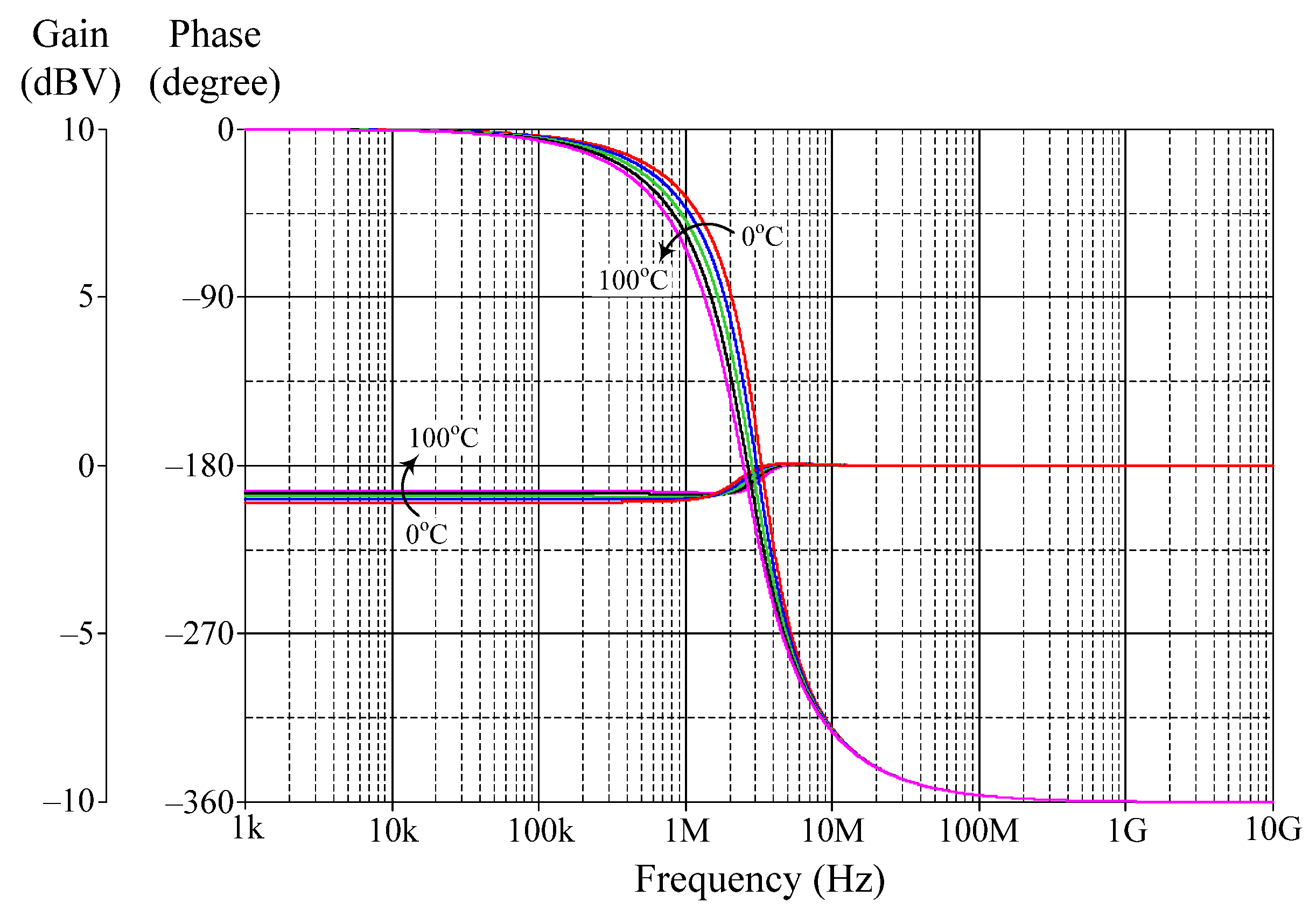
6. Simulation Results

In this section, a PSPICE simulation program was carried out to demonstrate the performance of the proposed configurations in Figure 3 and Figure 4. The VDGA was simulated using the CMOS circuit of Figure 2 with TSMC 0.18 μm transistor parameters, and with symmetrical supply voltages of ±0.9 V. Table 2 illustrates the aspect ratios of the CMOS transistors employed for the VDGA circuit in Figure 2. The capacitor settings for global simulations were C1 = C2 = 50 pF.

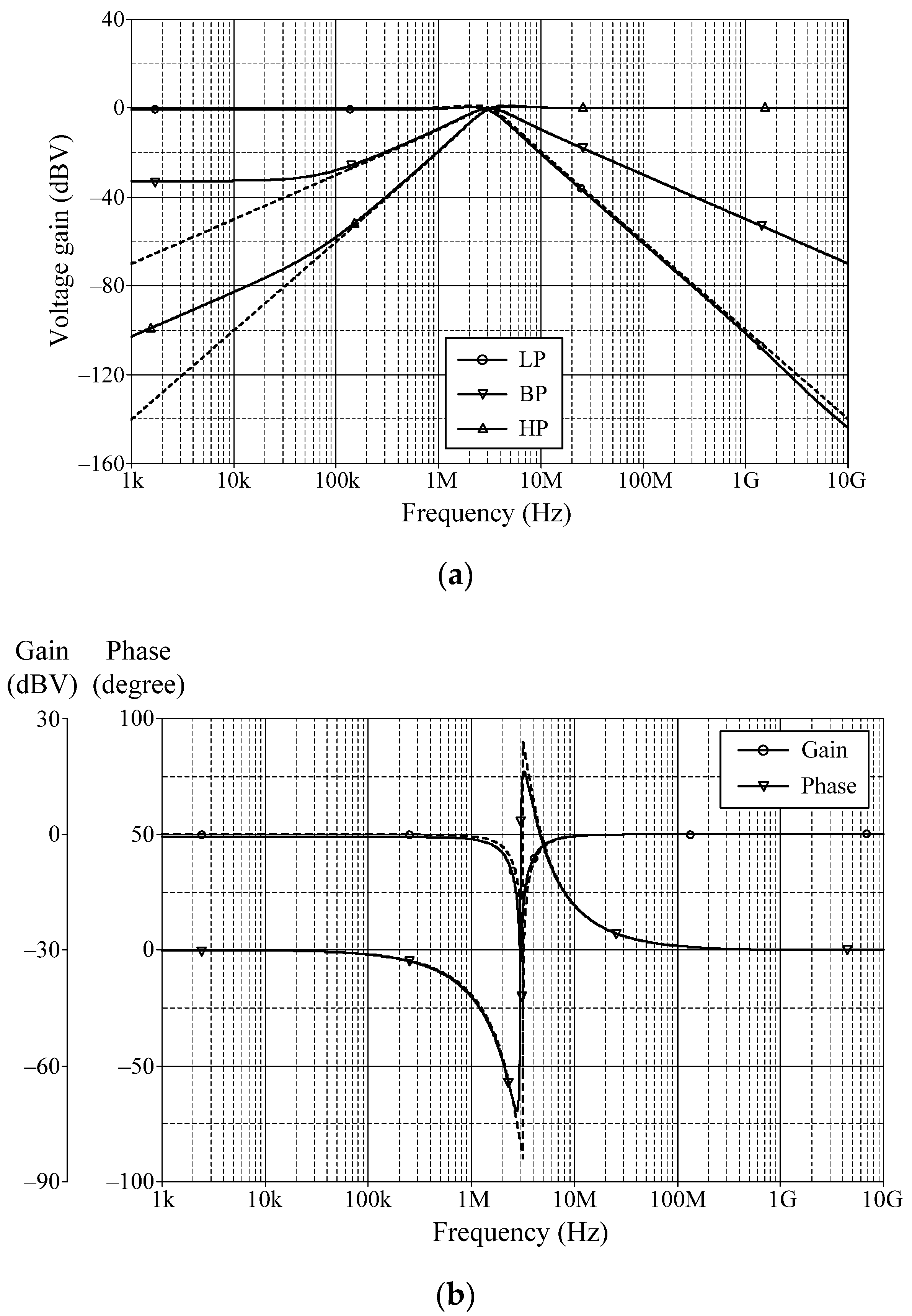
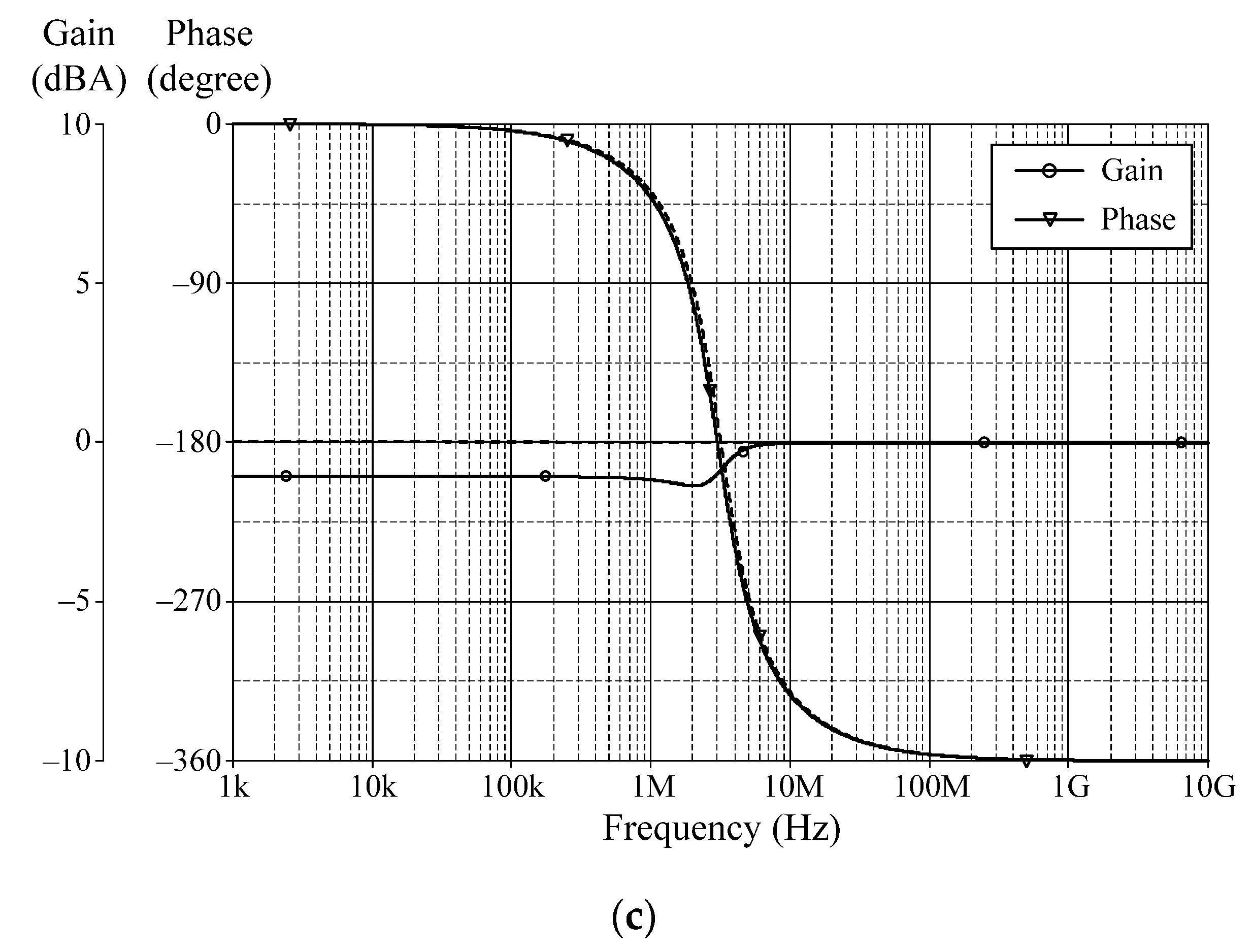
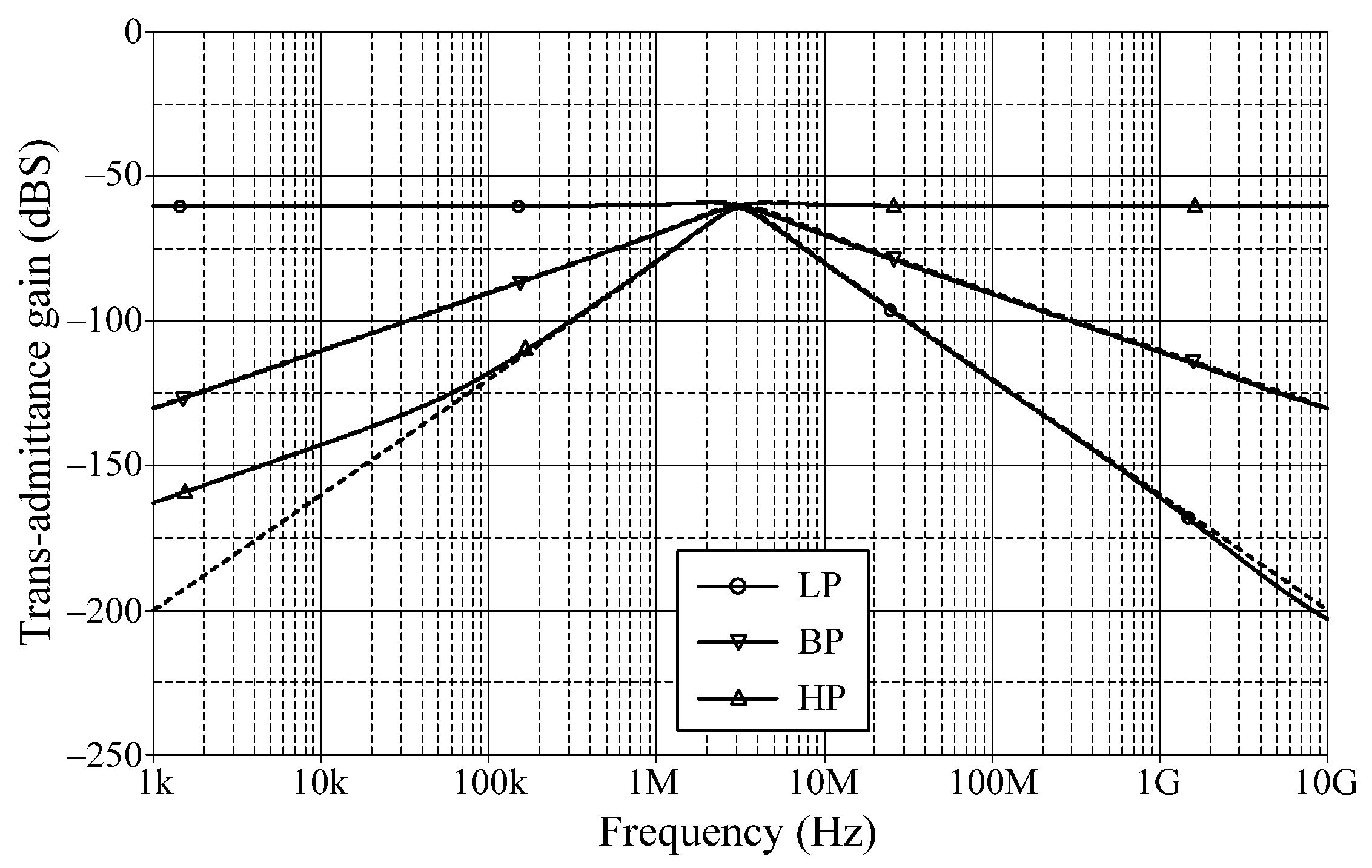
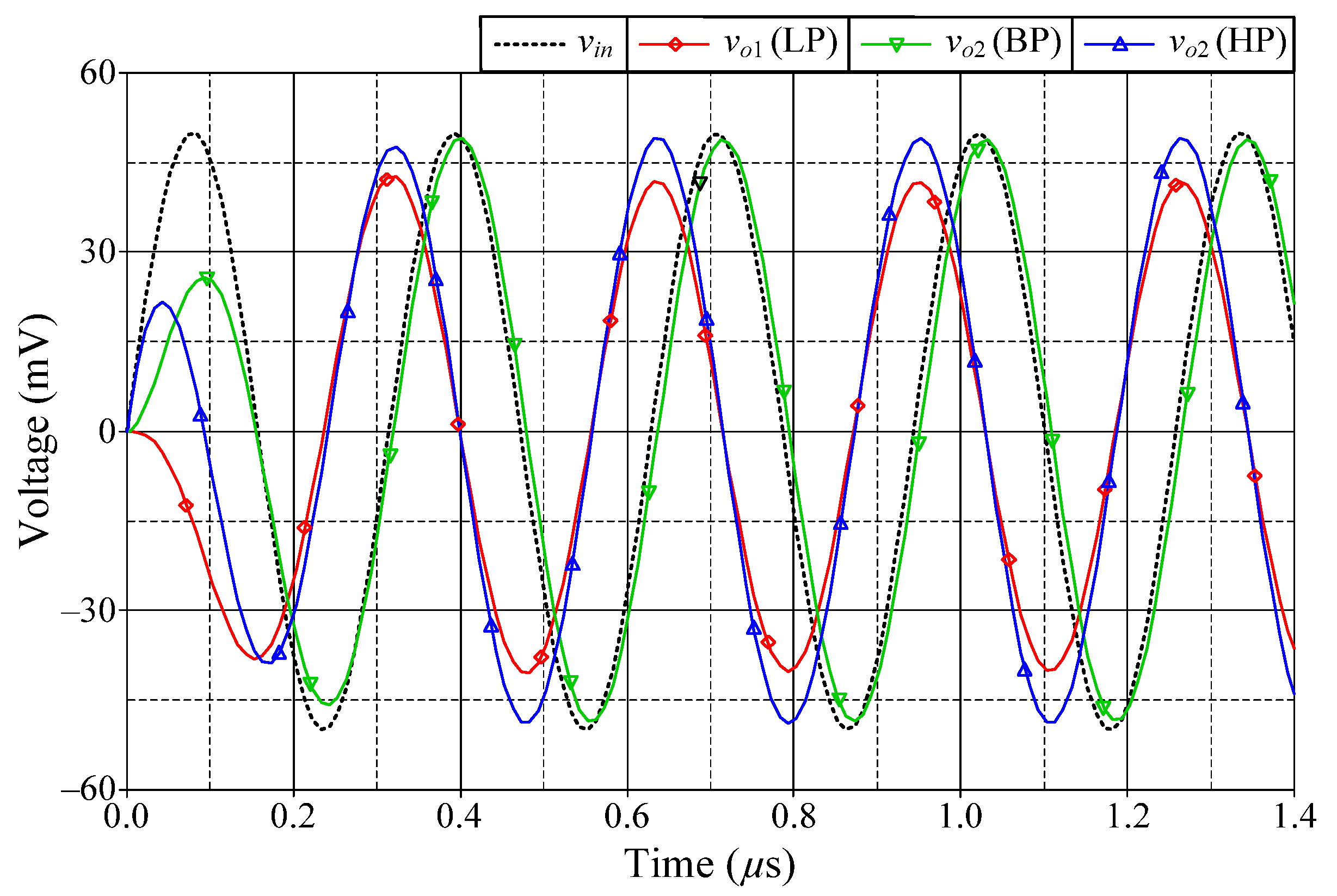
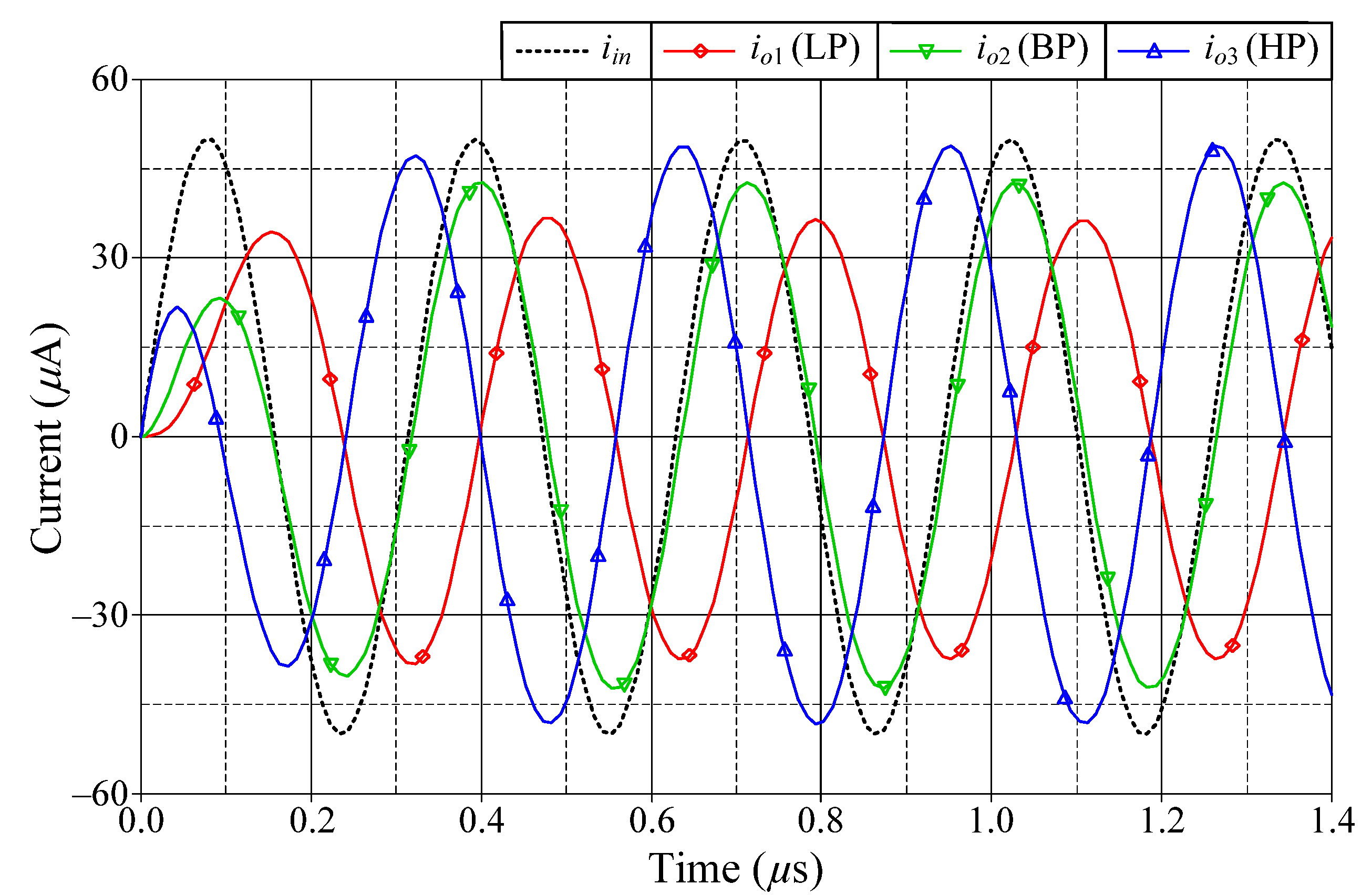
6.1. Simulation Verifications of the Proposed Mixed-Mode Universal Filter

The suggested mixed-mode universal filter in Figure 3 was performed with gmA = gmB = gmC = 1 mA/V (IBA = IBB = IBC = 80 μA), and R = 1 kΩ, to actualize all the four-mode universal filter responses with fo = 3.18 MHz and Q = 1. Figure 6, Figure 7, Figure 8 and Figure 9 illustrate the simulated and theoretical frequency responses of VM, CM, TAM, and TIM filters, respectively. The disparity between simulated and theoretical gain responses in the HP filters of VM, CM, and TAM, as well as the BP filter of TIM, is greater in the low-frequency range of roughly 1 kHz to 100 kHz. This phenomenon may be explained by the fact that the input or output signals of the circuits were sensed with C2 and R, introducing an undesirable pole that caused significant deviations in low operating frequencies. In Figure 6c and Figure 7c, the phase shifting between input and output signals was measured as −190.70° and −192.74°, respectively, and the gain response was 0.84 dBV and 1.067 dBA down from zero for the frequency ranges varying from 1 kHz to 1 MHz. The simulated fo and corresponding percentage errors are given in Table 3. It is to be observed that all simulation results are found to be in good consistent with the theoretical values. Figure 10, Figure 11, Figure 12 and Figure 13 depict the transient responses of the proposed filter to the following input signals: (i) a 3.18 MHz sinusoidal input voltage signal with an amplitude of 100 mV (peak-to-peak) applied to the VM and TAM filters; and (ii) 3.18 MHz sinusoidal input current signal with an amplitude of 100 μA (peak-to-peak) applied to the CM and TIM filters. Table 4 shows the total harmonic distortions (THDs) and DC components of the VM, CM, TAM, and TIM outputs in Figure 10, Figure 11, Figure 12 and Figure 13. As can be seen, the THD value is less than 1.92% in all four modes. Thus, there is no significant distortion in the biquad design. The entire power consumption of the circuit was 1.31 mW at ±0.9 V biased voltages.
In addition, the orthogonal tunability of a high-Q value for a BP filter in VM is shown in Figure 14. The filter is designed to operate at fo = 3.18 MHz with gmA = gmB = gmC = 1 mA/V. By simply adjusting the R value for 0.5 kΩ, 10 kΩ, and 50 kΩ, the BP responses with various Q values of 0.5, 10, and 50 are achieved, respectively. Based on the measured data, the Q value was evaluated as 0.495, 8.273, and 44.25, respectively. The relative variation of the Q factor remained less than 12%, even when Q reached 50.
The effect of temperature variation on the filter parameters is now being investigated. For this purpose, the proposed filter was simulated under ambient temperature changes ranging from 0 to 100 °C with a step of 25 °C. Figure 15 demonstrates the gain and phase variations of the AP filter in VM operation. The findings reveal that, for different temperatures, the gain and phase at fo vary from −0.44 to −0.5 dBV and from −172 to −223°, respectively.

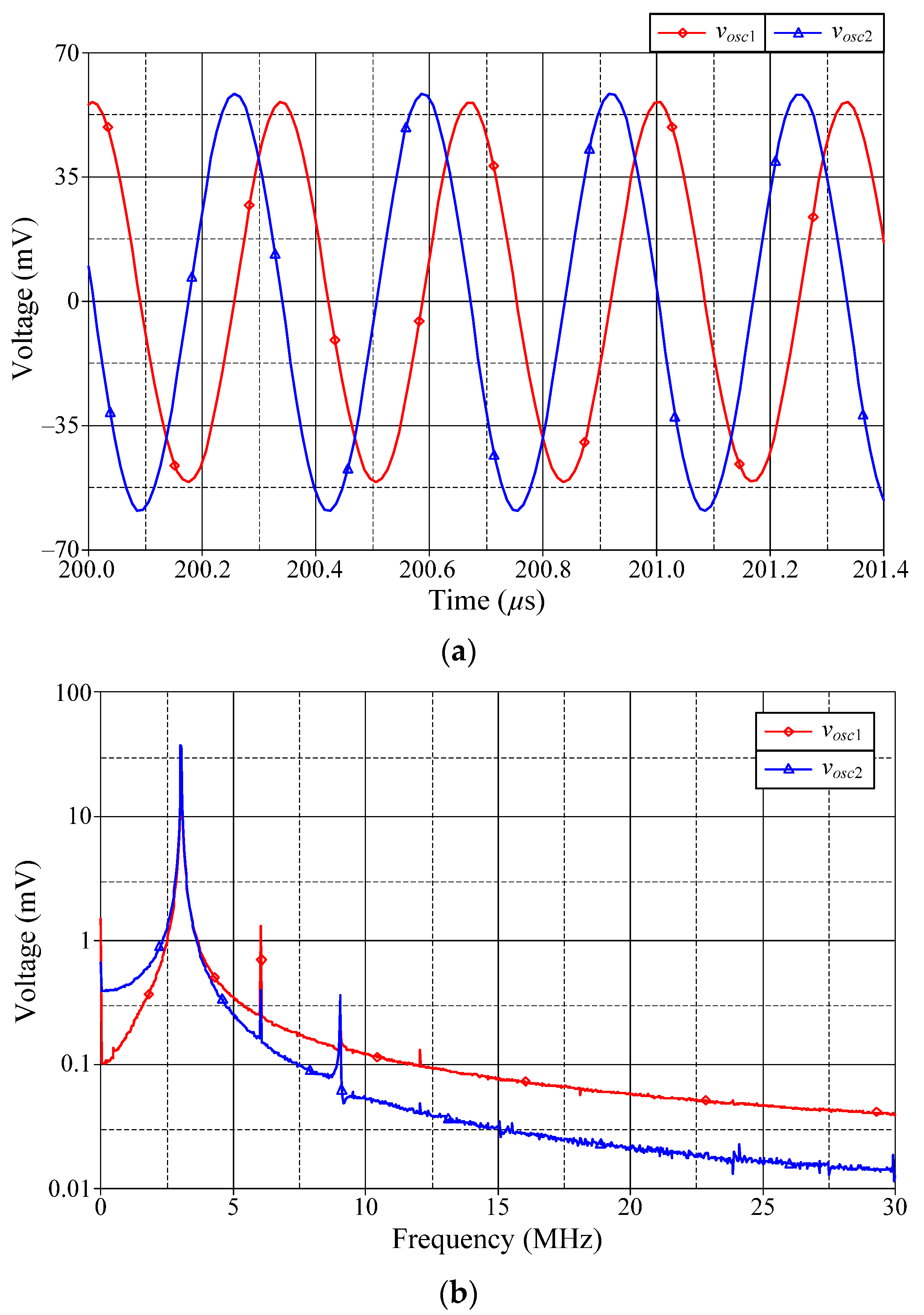
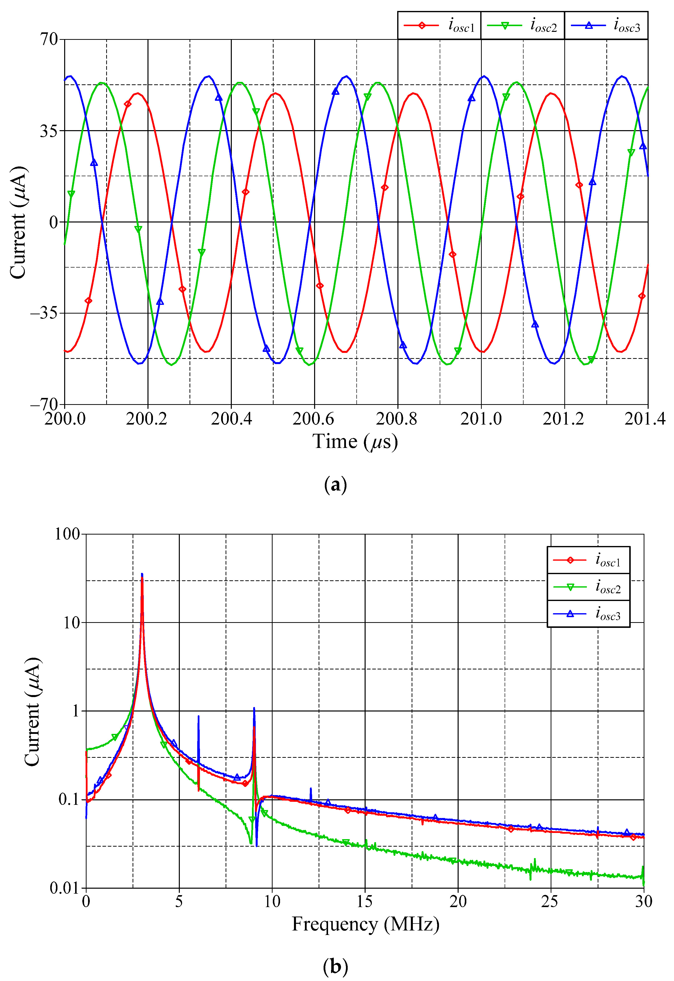
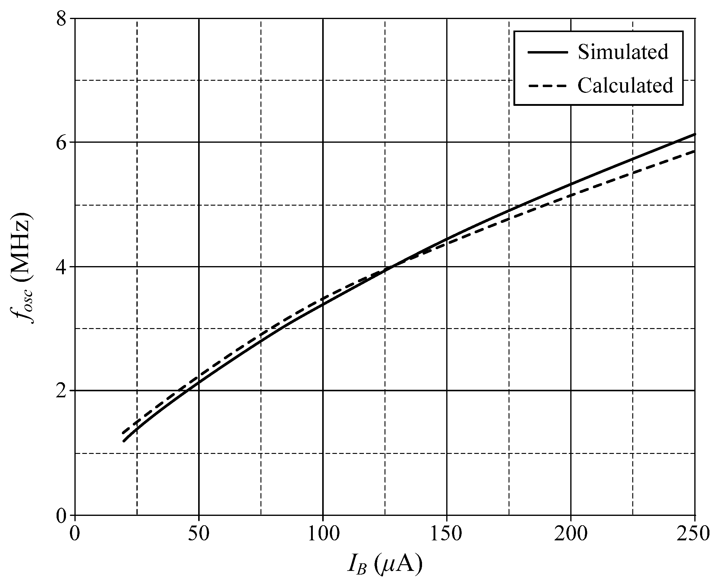
6.2. Simulation Verifications of the Proposed Dual-Mode Quadrature Oscillator

Based on previous component settings, the simulated quadrature voltages vosc1 and vosc2 of the proposed dual-mode quadrature oscillator in Figure 4 are displayed in Figure 16. Figure 16a shows the steady-state waveforms of vosc1 and vosc2, whereas Figure 16b presents the frequency spectrums of the oscillation output voltages. As per the findings, the simulated fosc was found to be 2.76 MHz, and the phase shift between vosc1 and vosc2 was 85.76°. The attenuations at the second harmonic for vosc1 and vosc2 were 30.30 dBm and 31.45 dBm, respectively. Further, the percentage of THD was 2.46% for vosc1 and 4.28% for vosc2.
Similarly, the simulated steady-state responses and the corresponding frequency spectrums of iosc1, iosc2, and iosc3 are also given in Figure 17. The phase shifts between iosc1 and iosc2, and iosc1 and iosc3 were measured to be 92.73° and 177.82°, respectively. The second-harmonic attenuations for iosc1, iosc2, and iosc3 were 30.05 dBμ, 30.88 dBμ, and 30.87 dBμ, respectively, while the percentage THDs of iosc1, iosc2, and iosc3 were 3.86%, 4.16%, and 3.50%, respectively.
Due to the VDGA transconductance gain gmk is tuned by the bias current IBk, the fosc of the proposed circuit is a current tunable function. Figure 18 demonstrates the calculation and simulation results for the variations of fosc as a function of IB, where IB = IBA = IBB = IBC.

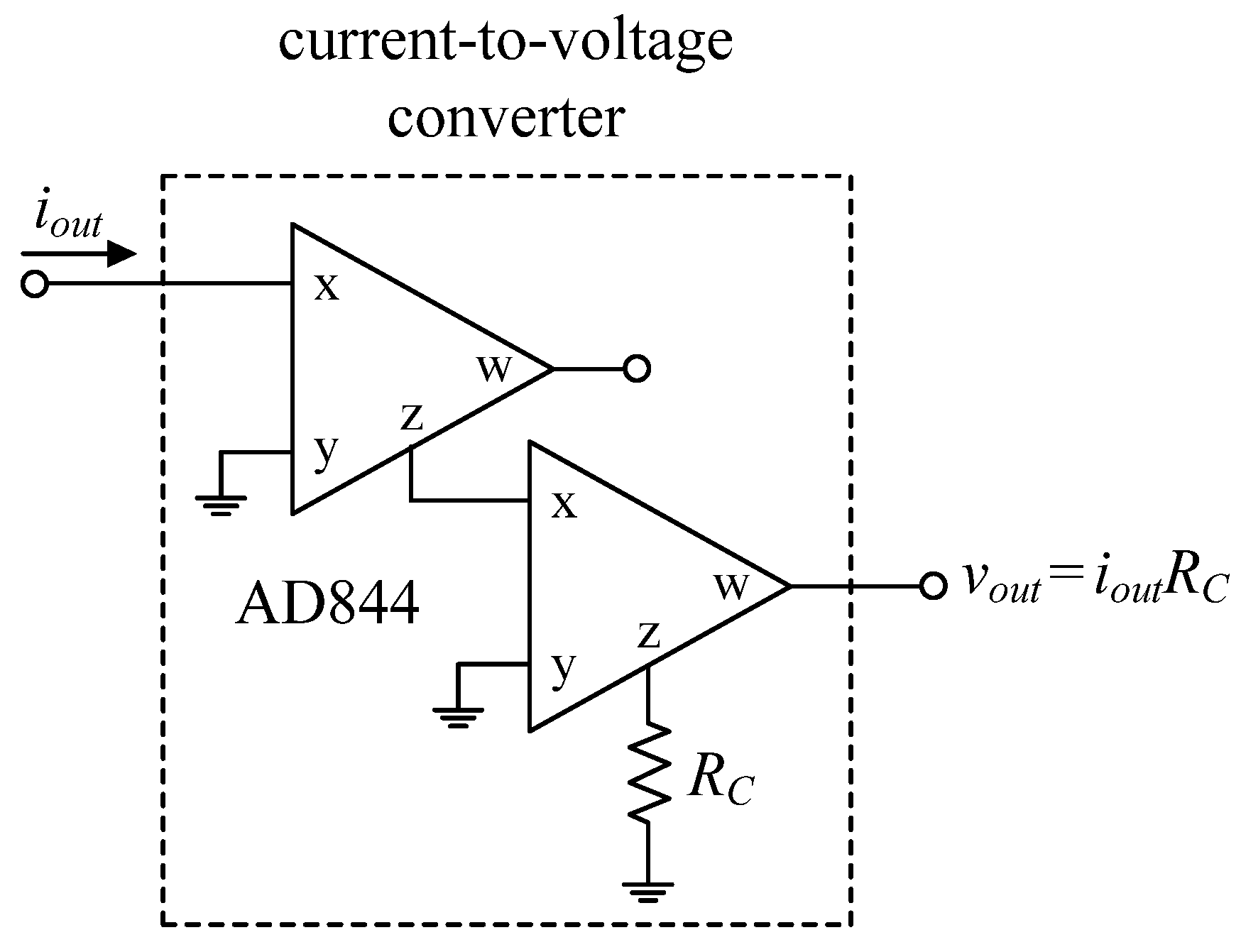
7. Experimental Results

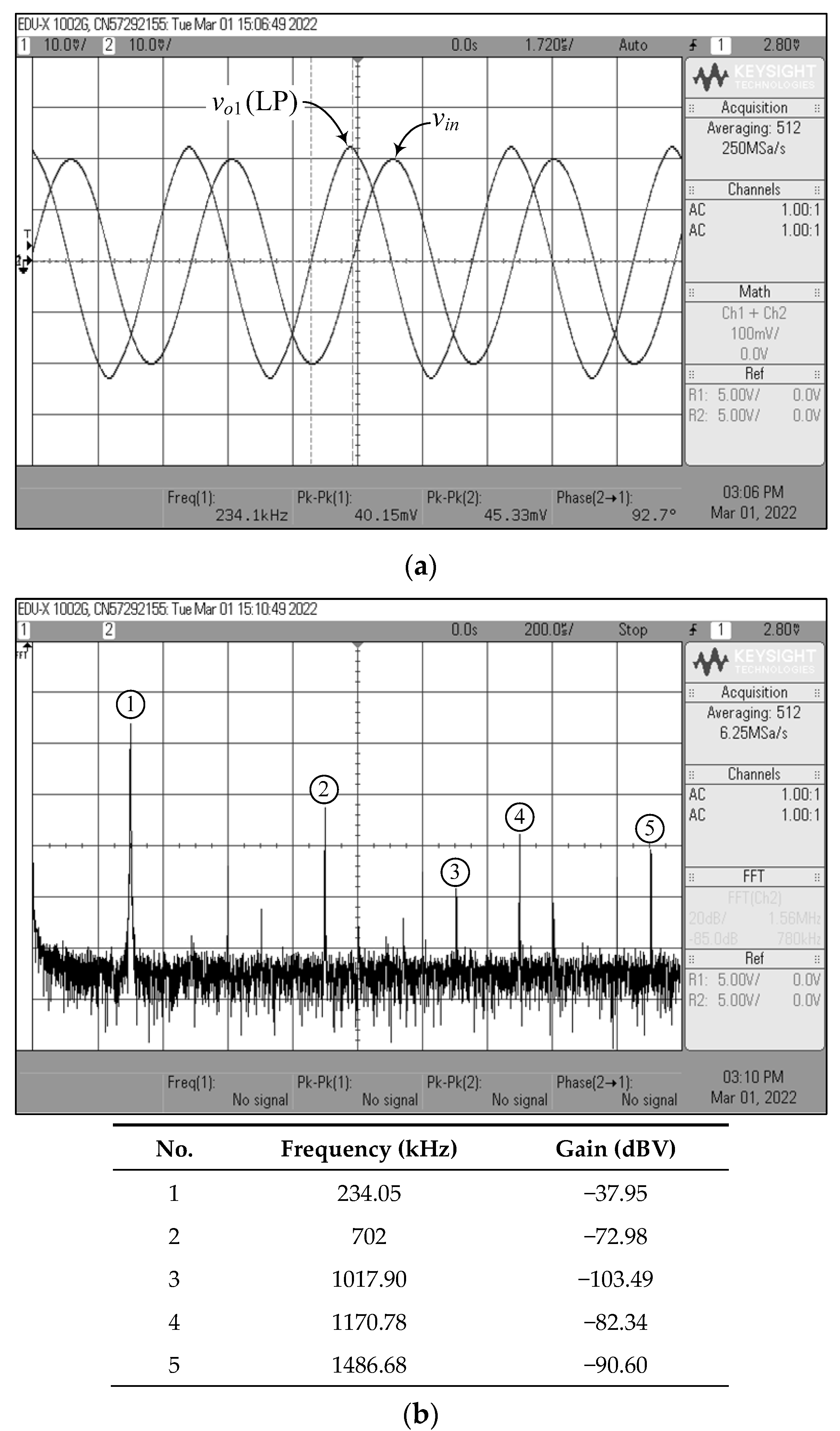
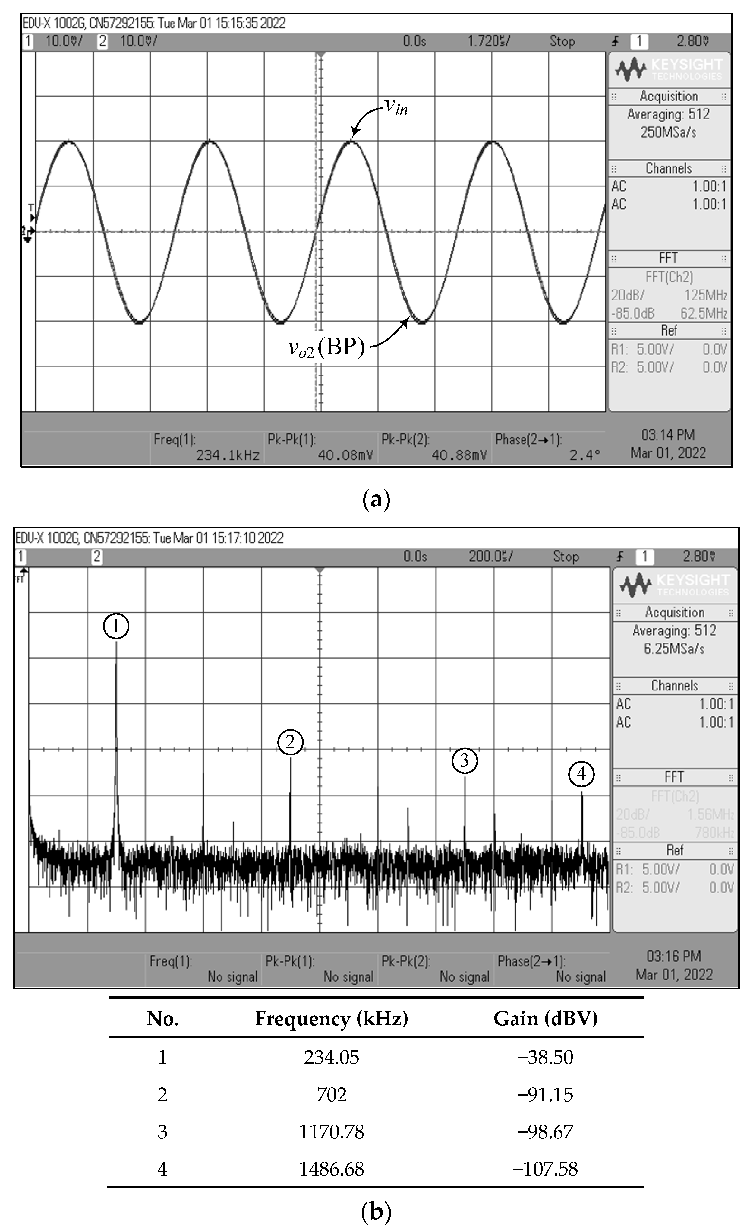
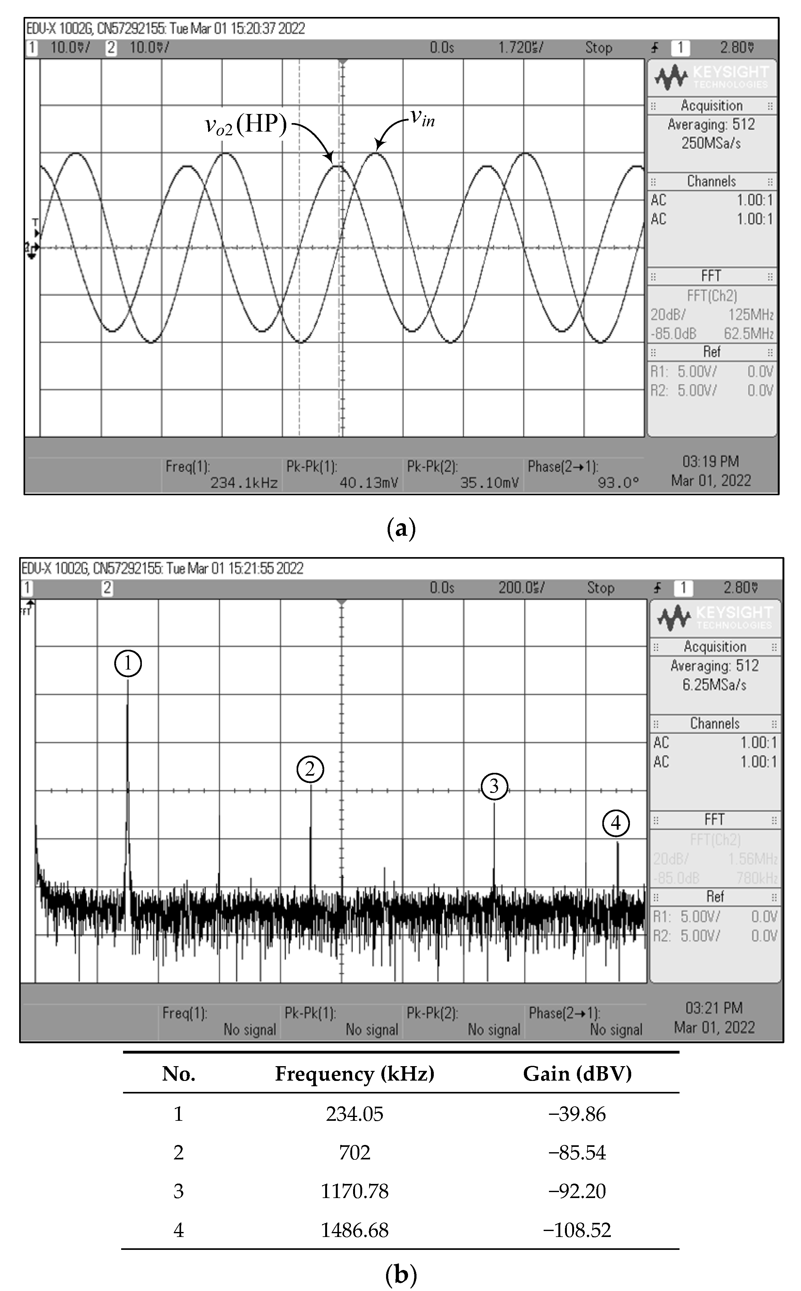
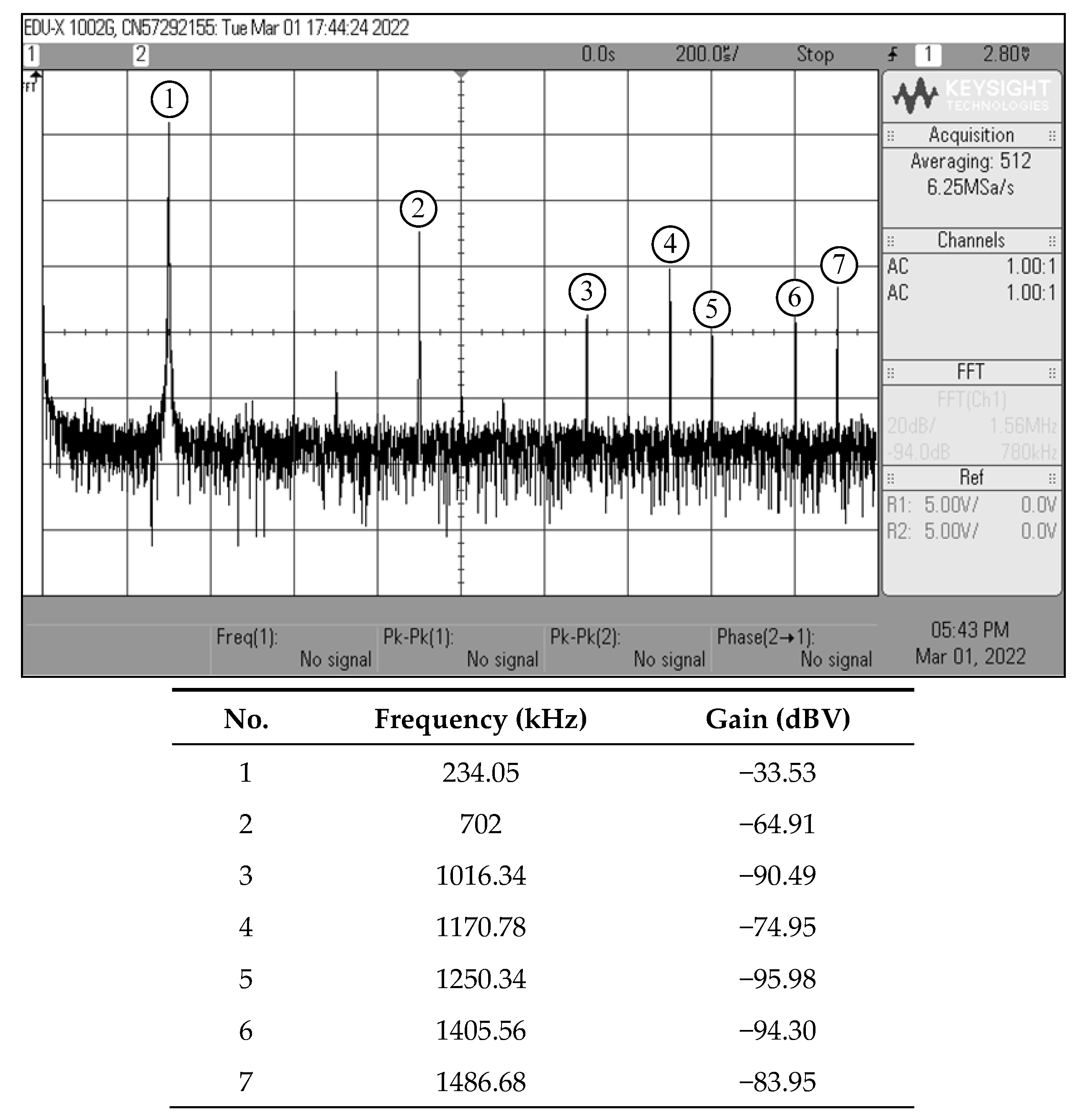
7.1. Experimental Verifications of the Proposed Mixed-Mode Universal Filter

To further support the theory, the suggested circuits in Figure 3 and Figure 4 were experimentally verified. As shown in Figure 19, the VDGA was built-in hardware utilizing off-the-shelf IC dual-OTA LM13600s from National Semiconductor [58]. To bias the LM13600, DC supply voltages of ±5 V were employed. A prototype hardware setup for verification purposes of the proposed circuit is illustrated in Figure 20. The component values were set as follows: gmA = gmB = gmC = 1 mA/V (IBA = IBB = IBC = 50 μA), R = 1 kΩ, and C1 = C2 = 680 pF, actually results in fo = 234 kHz, and Q = 1. In order to measure the input signals for the CM and TIM, a voltage-to-current converter with IC AD844 [59] and a converting resistor RC of 1 kΩ was used, as illustrated in Figure 21. In Figure 22, two extra AD844s and RC were used as a current-to-voltage conversion for output signal measurements in CM and TAM operations.
Figure 23, Figure 24, Figure 25, Figure 26 and Figure 27 show the measurements of the input and output waveforms and the relevant output spectrums for the proposed VM filter with a 20 mV (peak) sinewave input voltage at 234 kHz. The THD values of the LP, BP, HP, BS, and AP output responses were 1.88%, 0.25%, 0.57%, 1.84%, and 2.66%, respectively. As can be seen from Figure 23b, Figure 24b, Figure 25b, Figure 26b and Figure 27b, the spurious-free dynamic range (SFDR) for the cases of LP, BP, HP, BS, and AP were measured at 35.03 dBc, 52.65 dBc, 45.68 dBc, 36.35 dBc, and 34.33 dBc, respectively. Figure 28 also shows the experimental gain-frequency responses of the proposed VM filter. The measured results of fo of VM, CM, TAM, and TIM were found to be 241.13 kHz (error ~+3%), 227.08 kHz (error ~−2.98%), 227.38 kHz (error ~−2.87%), and 233.32 kHz (error ~−0.33%), respectively. In all cases, the practically observed behavior of the circuit was found to be consistent with the theoretical predictions. The experimental test results, thus, verify the practicability of the suggested design. Nevertheless, one observes that the discrepancy between the theoretical and measured results was originally caused by non-ideal gain and parasitic impedance effects of the LM13600s and AD844s. The stray capacitances generated by the breadboard circuit realization also affect the frequency performance of the circuit in experimental testing.

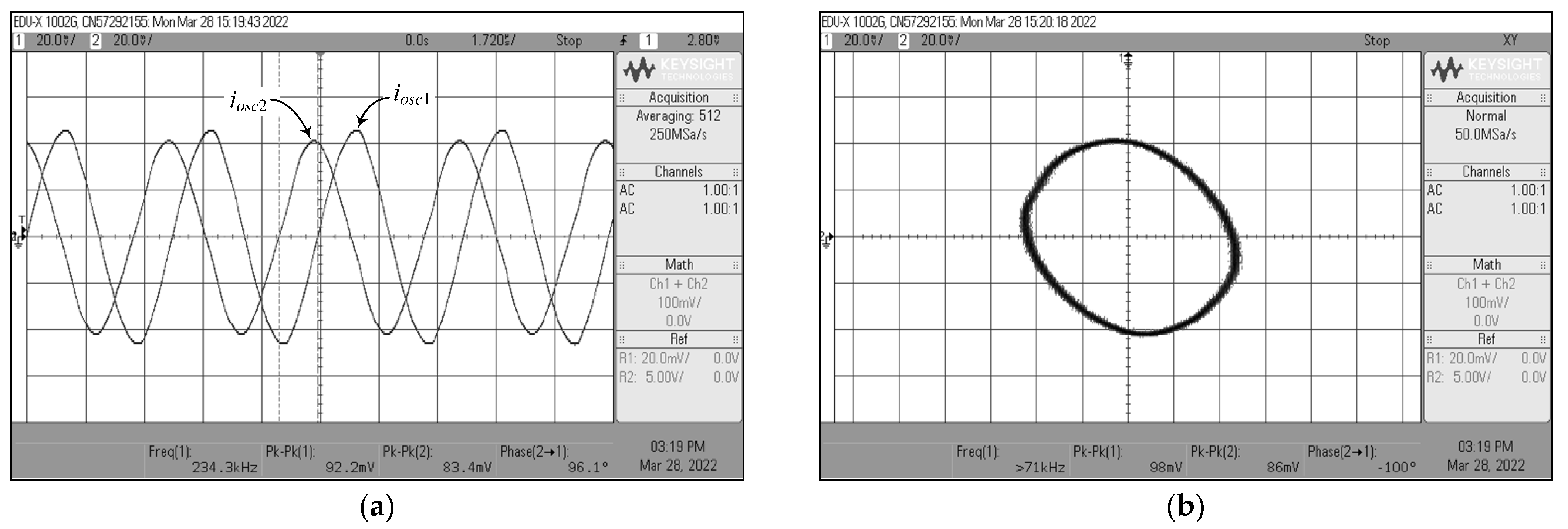
7.2. Experimental Verifications of the Proposed Dual-Mode Quadrature Oscillator

According to the experimental measurements for the proposed dual-mode quadrature oscillator in Figure 4, the oscilloscope output waveforms in time-domain and Lissajous pattern of vosc1 and vosc2 are given in Figure 29. By using the same component values as in the previous filter case, the oscillator was constructed to oscillate at an OF of fosc = 234 kHz. The fosc observed was 234.1 kHz, which is extremely close to the theoretical value. The phase angle difference between vosc1 and vosc2 was roughly 95.1°, resulting in an absolute phase deviation of 5.67%. Figure 30 also shows the measured frequency spectrum of the vosc1 output. From the experimental testing, the THD and SFDR values for the output vosc1 were 2.85% and 31.38 dBc, respectively.
For iosc1, iosc2, and iosc3 measurements, the current-to-voltage converter circuit as shown in Figure 22 was also employed. The time-domain waveforms and the corresponding Lissajous figures of the oscillator output currents iosc1 and iosc2, and iosc2 and iosc3 are illustrated in Figure 31 and Figure 32, respectively. The quadrature-phase shifts between iosc1 and iosc2, and iosc2 and iosc3 were 96.1° and 85.3°, respectively, deviating from the calculations by 6.78% and 5.22%. The frequency spectrum of the iosc1 output was also recorded and exhibited in Figure 33, with percentage THD and SFDR values of 2.05% and 34 dBc, respectively. Clearly, the generated waveforms observed in the experimental data validate the quadrature relationship of the suggested quadrature oscillator in both VM and CM.

8. Discussion

At this point, we would like to briefly discuss the superiority of the proposed MUBF and DMQO design over similar existing designs in the literature. The following observations are based on Table 1.
In contrast to the topologies in [1,2,3,4,5,6,7,8,9,10,11,12,13,14,15,16,17,18,19,20,21,22,23,24,25,26,27,28,29,30,31,32,33,34,35,36,37,38,39,40], the proposed circuit uses the same topology to perform both MUBF and DMQO, whereas the works referenced only perform MUBF [1,2,3,4,5,6,7,8,9,10,11,12,13,14,15,16,17,18,19,20,21,22,23,24,25,26,27,28,29,30,31] or DMQO [32,33,34,35,36,37,38,39,40]. With regard to the MUBF topologies introduced in [5,7,9,10,12,13,14,15,18,22,23,25,26,27,30], all five biquadratic filter functions are implemented in all four modes of operation. These circuits, however, employ more active components, especially at least two active components, than the suggested circuit. Some have three or more passive components [9,12,13,14,15,22,23,24,25,26,27,28,29,30,31] or DMQO [32,33]. In addition to the filters of [2,6,8,11,16,19,20,24], they are limited to only two modes of operation. Designing with a low component count is a simple technique to reduce the total power consumption of the designed circuit. Even though compact MUBF circuits implemented with a single active element have been proposed in [3,8,16,21,24,27,28,41,48], these biquads still use more passive elements than the MUBF circuit proposed in this work. While the designs described in [4,7,12,14,15,18,19,20,23,26,45,49,50] are interesting, they suffer from the usage of two or more different types of active components, which complicates circuit implementation.
In the QO configurations [47,48], there are floating passive elements that are not encouraged for further integration. Several QO designs operated in either VM [44,47,49] or CM [42,43]. As compared to the proposed DMQO circuit, it not only uses grounded passive elements, but it also provides both voltage and current quadrature outputs simultaneously.
The topologies in [1,2,6,7,8,10,13,18,21,23,28,31,40,42,43,48,50] do not offer independent adjustment of their important parameters, but even the proposed MUBF and DMQO design allows independent parameter modification through transconductance (gm) or single resistance value. Also in the existing literature [2,3,4,6,8,9,12,13,19,22,23,31,32,34,39,47], an electronic control of various parameters is not available.
As a conclusion, it should be noted that the proposed MUBF and DMQO circuit in this study is capable of fulfilling all of the performance features described above simultaneously and without trade-offs.

9. Conclusions

This work proposes a compact mixed-mode universal biquadratic filter and dual-mode quadrature oscillator circuit using a single voltage differencing gain amplifier (VDGA). In this design, a canonical structure with one resistor and two capacitors is employed. The proposed universal biquad filter is able to realize generic second-order filter functions in all four modes of operation, namely, VM, CM, TAM, and TIM. It has the feature of orthogonal control of ωo and Q characteristics, and simultaneously the ability to implement a high-Q filter with a single resistance adjustment. The quadrature oscillator, which generates both voltage and current output signals simultaneously, is also feasible by slight modification of the proposed configuration. Both the oscillation condition and the oscillation frequency of the proposed quadrature oscillator are non-interactively controlled. The circuits are subjected to non-ideal analysis, including tracking error and parasitic element effects. The simulation and experimental findings prove that the suggested circuit performs in both the mixed-mode universal biquad filter and the dual-mode quadrature oscillator.

Author Contributions

Conceptualization, N.R. and W.T.; methodology, N.R. and W.T.; software, N.R. and T.P.; validation, N.R., W.T., and T.P.; formal analysis, N.R. and W.T.; investigation, N.R., W.T. and T.P.; resources, N.R. and W.T.; data curation, N.R., W.T. and T.P.; writing—original draft preparation, W.T.; writing—review and editing, W.T.; visualization, W.T. and T.P.; supervision, W.T.; project administration, W.T.; funding acquisition, N.R., W.T. and T.P. All authors have read and agreed to the published version of the manuscript.

Funding

This research received no external funding.

Institutional Review Board Statement

Not applicable.

Informed Consent Statement

Not applicable.

Data Availability Statement

The data supporting the results presented in this work are available on request from the authors.

Acknowledgments

This work was supported by King Mongkut’s Institute of Technology Ladkrabang (KMITL).

Conflicts of Interest

The authors declare no conflict of interest.

Symbols and Nomenclatures

The following symbols and nomenclatures are used in this manuscript:
VDGAvoltage differencing gain amplifier
VMvoltage-mode
CMcurrent-mode
TAMtrans-admittance-mode
TIMtrans-impedance-mode
LPlow-pass
BPband-pass
HPhigh-pass
BSband-stop
APall-pass
MUBFmixed-mode universal biquadratic filter
QOquadrature oscillator
DMQOdual-mode QO
OCoscillation condition
OFoscillation frequency
gmtransconductance gain of the VDGA
βvoltage transfer gain of the VDGA
µeffective channel electronic mobility
Coxgate-oxide capacitance per unit area
Weffective channel width
Leffective channel length
TVtransfer function of voltage-mode filter
TItransfer function of current-mode filter
TYtransfer function of trans-admittance-mode filter
TZtransfer function of trans-impedance-mode filter
ωonatural angular frequency of biquadratic filter
fonatural frequency of biquadratic filter
Qquality factor of biquadratic filter
ωoscnatural angular frequency of oscillator
foscfrequency of oscillator
ej90°Euler’s formula shows a 90° phase difference between two signals
ej180°Euler’s formula shows a 180° phase difference between two signals
αnon-ideal transconductance gain
δnon-ideal voltage transfer gain
εαtracking error of transconductance gain
εδtracking error of voltage transfer gain
dBVvoltage decibel
dBAampere decibel
dBSsiemens decibel
dBΩOhm decibel
dBmmili decibel
dBµmicro decibel
dBcdecibels relative to the carrier
THDtotal harmonic distortion
SFDRspurious-free dynamic range

References

  1. Abuelma’atti, M.T. A novel mixed-mode current-controlled current-conveyor-based filter. Act. Passiv. Electron. Compon. 2003, 26, 185–191. [Google Scholar] [CrossRef] [Green Version]
  2. Gupta, S.S.; Senani, R. New voltage-mode/current-mode universal biquad filter using unity-gain cells. Int. J. Electron. 2006, 93, 769–775. [Google Scholar] [CrossRef]
  3. Lee, C.N.; Chang, C.M. Single FDCCII-based mixed-mode biquad filter with eight outputs. AEU—Int. J. Electron. Commun. 2009, 63, 736–742. [Google Scholar] [CrossRef]
  4. Minaei, S.; Ibrahim, M.A. A mixed-mode KHN-biquad using DVCC and grounded passive elements suitable for direct cascading. Int. J. Circuit Theory Appl. 2009, 37, 793–810. [Google Scholar] [CrossRef]
  5. Chen, H.P.; Liao, Y.Z.; Lee, W.T. Tunable mixed-mode OTA-C universal filter. Analog Integr. Circuits Signal Process. 2009, 58, 135–141. [Google Scholar] [CrossRef]
  6. Horng, J.W. High-order current-mode and transimpedance-mode universal filters with multiple-inputs and two-outputs using MOCCIIs. Radioengineering 2009, 18, 537–543. [Google Scholar]
  7. Lee, C.N. Multiple-mode OTA-C universal biquad filters. Circuits Syst. Signal Process. 2010, 29, 263–274. [Google Scholar] [CrossRef]
  8. Yuce, E. Fully integrable mixed-mode universal biquad with specific application of the CFOA. AEU—Int. J. Electron. Commun. 2010, 64, 304–309. [Google Scholar] [CrossRef]
  9. Liao, W.B.; Gu, J.C. SIMO type universal mixed-mode biquadratic filter. Indian J. Eng. Mater. Sci. 2011, 18, 443–448. [Google Scholar]
  10. Pandey, N.; Paul, S.K. Mixed mode universal filter. J. Circuits Syst. Comput. 2013, 22, 1250064. [Google Scholar] [CrossRef]
  11. Yeşil, A.; Kaçar, F. Electronically tunable resistorless mixed mode biquad filters. Radioengineering 2013, 22, 1016–1025. [Google Scholar]
  12. Lee, C.N. Independently tunable mixed-mode universal biquad filter with versatile input/output functions. AEU—Int. J. Electron. Commun. 2016, 70, 1006–1019. [Google Scholar] [CrossRef]
  13. Lee, C.N. Mixed-mode universal biquadratic filter with no need of matching conditions. J. Circuits Syst. Comput. 2016, 25, 1650106. [Google Scholar] [CrossRef]
  14. Singh, D.; Afzal, N. Fully digitally programmable generalized mixed mode universal filter configuration. Circuits Syst. Signal Process. 2016, 35, 1457–1480. [Google Scholar] [CrossRef]
  15. Singh, D.; Afzal, N. Digitally programmable mixed mode universal filter using followers-a minimal realization. Analog Integr. Circuits Signal Process. 2016, 86, 289–298. [Google Scholar] [CrossRef]
  16. Pandey, R.; Pandey, N.; Singhal, N. Single VDTA based dual mode single input multioutput biquad filter. J. Eng. 2016, 2016, 1674343. [Google Scholar] [CrossRef] [Green Version]
  17. Chen, H.P.; Yang, W.S. Electronically tunable current controlled current conveyor transconductance amplifier-based mixed-mode biquadratic filter with resistorless and grounded capacitors. Appl. Sci. 2017, 7, 244. [Google Scholar] [CrossRef] [Green Version]
  18. Parvizi, M.; Taghizadeh, A.; Mahmoodian, H.; Kozehkanani, Z.D. A low-power mixed-mode SIMO universal GmC filter. J. Circuits Syst. Comput. 2017, 26, 1750164. [Google Scholar] [CrossRef]
  19. Horng, J.W.; Wu, C.M.; Herencsar, N. Current-mode and transimpedance-mode universal biquadratic filter using two current conveyors. Indian J. Eng. Mater. Sci. 2017, 24, 461–468. [Google Scholar]
  20. Cini, U.; Aktan, M. Dual-mode OTA based biquadratic filter suitable for current-mode applications. AEU—Int. J. Electron. Commun. 2017, 80, 43–47. [Google Scholar] [CrossRef]
  21. Faseehuddin, M.; Sampe, J.; Shireen, S.; Ali, S.H.M. A novel mix-mode universal filter employing a single active element and minimum number of passive components. Inf. MIDEM 2017, 47, 211–221. [Google Scholar]
  22. Chaturvedi, B.; Mohan, J.; Kumar, A. A new versatile universal biquad configuration for emerging signal processing applications. J. Circuits Syst. Comput. 2018, 27, 1850196. [Google Scholar] [CrossRef]
  23. Safari, L.; Barile, G.; Ferri, G.; Stornelli, V. A new low-voltage low-power dual-mode VCII-based SIMO universal filter. Electronics 2019, 8, 765. [Google Scholar] [CrossRef] [Green Version]
  24. Albrni, M.A.; Faseehuddin, M.; Sampe, J.; Ali, S.H.M. Novel dual mode multifunction filter employing highly versatile VD-DXCC. Inf. MIDEM 2019, 49, 169–176. [Google Scholar] [CrossRef]
  25. Bhaskar, D.R.; Raj, A.; Kumar, P. Mixed-mode universal biquad filter using OTAs. J. Circuits Syst. Comput. 2020, 29, 2050162. [Google Scholar] [CrossRef]
  26. Albrni, M.I.A.; Mohammad, F.; Herencsar, N.; Sampe, J.; Ali, S.H.M. Novel electronically tunable biquadratic mixed-mode universal filter capable of operating in MISO and SIMO configurations. Inf. MIDEM 2020, 50, 189–203. [Google Scholar] [CrossRef]
  27. Mohammad, F.; Herencsar, N.; Albrni, M.A.; Sampe, J. Electronically tunable mixed mode universal filter employing a single active block and a minimum number of passive components. Appl. Sci. 2021, 11, 55. [Google Scholar] [CrossRef]
  28. Agrawal, D.; Maheshwari, S. High-performance electronically tunable analog filter using a single EX-CCCII. Circuits Syst. Signal Process. 2021, 40, 1127–1151. [Google Scholar] [CrossRef]
  29. Roongmuanpha, N.; Faseehuddin, M.; Herencsar, N.; Tangsrirat, W. Tunable mixed-mode voltage differencing buffered amplifier-based universal filter with independently high-Q factor controllability. Appl. Sci. 2021, 11, 9606. [Google Scholar] [CrossRef]
  30. Faseehuddin, M.; Herencsar, N.; Shireen, S.; Tangsrirat, W.; Md Ali, S.H. Voltage differencing buffered amplifier-based novel truly mixed-mode biquadratic universal filter with versatile input/output features. Appl. Sci. 2022, 12, 1229. [Google Scholar] [CrossRef]
  31. Unuk, T.; Yuce, E. A mixed-mode filter with DVCCs and grounded passive components only. AEU—Int. J. Electron. Commun. 2022, 144, 154063. [Google Scholar] [CrossRef]
  32. Horng, J.W.; Hou, C.L.; Chang, C.M.; Chou, H.P.; Lin, C.T.; Wen, Y.H. Quadrature oscillators with grounded capacitors and resistors using FDCCIIs. ETRI J. 2006, 28, 486–493. [Google Scholar] [CrossRef]
  33. Lahiri, A. Novel voltage/current-mode quadrature oscillator using current differencing transconductance amplifier. Analog Integr. Circuits Signal Process. 2009, 61, 199–203. [Google Scholar] [CrossRef]
  34. Maheshwari, S. Quadrature oscillator using grounded components with current and voltage outputs. IET Circuits Devices Syst. 2009, 3, 153–160. [Google Scholar] [CrossRef]
  35. Chen, H.P.; Wang, S.F.; Hsieh, M.Y. Tunable current-mode and voltage-mode quadrature oscillator using a DVCCTA. IEICE Electron. Express 2014, 11, 1–16. [Google Scholar] [CrossRef] [Green Version]
  36. Tangsrirat, W. Dual-mode sinusoidal quadrature oscillator with single CCTA and grounded capacitors. Inf. MIDEM 2016, 46, 130–135. [Google Scholar]
  37. Srivastaya, M.; Prasad, D. VDCC based dual-mode sinusoidal quadrature oscillator with outputs at appropriate impedance. Theor. Appl. Electr. Eng. 2016, 14, 168–177. [Google Scholar] [CrossRef]
  38. Tangsrirat, W. Compact quadrature oscillator with voltage and current outputs using only single VDTA and grounded capacitors. Indian J. Pure Appl. Phys. 2017, 55, 254–260. [Google Scholar]
  39. Kumar, A.; Kushwaha, A.K.; Paul, S.K. Electronically tunable mixed mode quadrature oscillator using DX-MOCCII. J. Circuits Syst. Comput. 2021, 30, 2150006. [Google Scholar] [CrossRef]
  40. Channumsin, O.; Bhardwaj, K.; Srivastava, M.; Tangsrirat, W.; Petchmaneelumka, W. Single voltage differencing gain amplifier based dual-mode quadrature oscillator using only grounded passive components. Eng. Lett. 2022, 30, 255–260. [Google Scholar]
  41. Jaikla, W.; Siripruchyanun, M.; Lahiri, A. Resistorless dual-mode quadrature sinusoidal oscillator using a single active building block. Microelectron. J. 2011, 42, 135–140. [Google Scholar] [CrossRef]
  42. Jin, J.; Wang, C. Current-mode universal filter and quadrature oscillator using CDTAs. Turk. J. Electr. Eng. Comput. Sci. 2014, 22, 276–286. [Google Scholar] [CrossRef] [Green Version]
  43. Jin, J. Resistorless active SIMO universal filter and four-phase quadrature oscillator. Arab. J. Sci. Eng. 2014, 39, 3887–3894. [Google Scholar] [CrossRef]
  44. Tuntrakool, S.; Kumngern, M.; Sotner, R.; Herencsar, N.; Suwanjan, P.; Jaikla, W. High Input Impedance Voltage-Mode Universal Filter and Its Modification as Quadrature Oscillator Using VDDDAs. Indian J. Pure Appl. Phys. 2017, 55, 324–332. [Google Scholar]
  45. Gupta, M.; Arora, T.S. Realization of current mode universal filter and a dual-mode single resistance controlled quadrature oscillator employing VDCC and only grounded passive elements. Adv. Electr. Electron. Eng. 2018, 15, 833–845. [Google Scholar] [CrossRef]
  46. Kumngern, M.; Khateb, F. Current-mode universal filter and quadrature oscillator using current controlled current follower transconductance amplifiers. Analog Integr. Circuits Signal Process. 2019, 100, 235–248. [Google Scholar] [CrossRef]
  47. Yucel, F.; Yuce, E. Supplementary CCII based second-order universal filter and quadrature oscillators. AEU—Int. J. Electron. Commun. 2020, 118, 153138. [Google Scholar] [CrossRef]
  48. Tangsrirat, W.; Pukkalanun, T.; Channumsin, O. Single VDGA-based dual-mode multifunction biquadratic filter and quadrature sinusoidal oscillator. Inf. MIDEM 2020, 50, 125–136. [Google Scholar] [CrossRef]
  49. Kumngern, M.; Khateb, F.; Kulej, T.; Psychalinos, C. Multiple-input universal filter and quadrature oscillator using multiple-input operational transconductance amplifiers. IEEE Access 2021, 9, 56253–56263. [Google Scholar] [CrossRef]
  50. Arora, T.S.; Gupta, M.; Gupta, S.N. An explicit output current-mode quadrature sinusoidal oscillator and a universal filter employing only grounded passive components-a minimal realization. Adv. Electr. Electron. Eng. 2021, 19, 258–271. [Google Scholar] [CrossRef]
  51. Satansup, J.; Tangsrirat, W. CMOS realization of voltage differencing gain amplifier (VDGA) and its application to biquad filter. Indian J. Eng. Mater. Sci. 2013, 20, 457–464. [Google Scholar]
  52. Taskiran, Z.G.C.; Sedef, H.; Anday, F. Voltage differencing gain amplifier-based nth-order low-pass voltage-mode filter. J. Circuit Syst. Comp. 2018, 27, 1850089. [Google Scholar] [CrossRef]
  53. Tangsrirat, W.; Pukkalanun, T.; Channumsin, O. Dual-mode multifunction filter realized with single voltage differencing gain amplifier (VDGA). Eng. Rev. 2021, 41, 1–14. [Google Scholar] [CrossRef]
  54. Channumsin, O.; Tangsrirat, W. Compact electronically tunable quadrature oscillator using single voltage differencing gain amplifier (VDGA) and all grounded passive elements. Turk. J. Electr. Eng. Comp. Sci. 2017, 25, 2686–2695. [Google Scholar] [CrossRef]
  55. Channumsin, O.; Tangsrirat, W. Voltage differencing gain amplifier-based sinusoidal quadrature oscillator using only two grounded capacitors. Recent Adv. Electr. Electron. Eng. 2019, 12, 439–444. [Google Scholar] [CrossRef]
  56. Tangsrirat, W.; Channumsin, O.; Pimpol, J. Electronically adjustable capacitance multiplier circuit with a single voltage differencing gain amplifier (VDGA). Inf. MIDEM 2019, 49, 211–217. [Google Scholar]
  57. Arbel, A.F.; Goldminz, L. Output stage for current-mode feedback amplifiers, theory and applications. Analog Integr. Circuits Signal Process. 1992, 2, 243–255. [Google Scholar] [CrossRef]
  58. National Semiconductor, LM13600: Dual Operational Transconductance Amplifiers with Linearizing Diodes and Buffers. Available online: https://pdf1.alldatasheet.com/datasheet-pdf/view/8640/NSC/LM13600N.html (accessed on 31 May 2022).
  59. Analog Devices, AD844: 60 MHz, 2000 V/μs, Monolithic op amp with Quad Low Noise. Available online: https://www.analog.com/media/en/technical-documentation/data-sheets/AD844.pdf (accessed on 29 June 2022).
Figure 1. Schematic representation of the VDGA.
Sensors 22 05303 g001
Figure 2. VDGA internal circuit implementation in CMOS technology.
Sensors 22 05303 g002
Figure 3. Proposed mixed-mode universal biquadratic filter.
Sensors 22 05303 g003
Figure 4. Proposed dual-mode quadrature oscillator.
Sensors 22 05303 g004
Figure 5. Non-ideal behavior model of the VDGA.
Sensors 22 05303 g005
Figure 6. Frequency characteristics for VM (simulated in solid line, theoretical in dashed line): (a) LP, BP, and HP; (b) BS; (c) AP.
Sensors 22 05303 g006aSensors 22 05303 g006b
Figure 7. Frequency characteristics for CM (simulated in solid line, theoretical in dashed line): (a) LP, BP, and HP; (b) BS; (c) AP.
Sensors 22 05303 g007aSensors 22 05303 g007b
Figure 8. LP, BP, and HP frequency characteristics for TAM (simulated in solid line, theoretical in dashed line).
Sensors 22 05303 g008
Figure 9. LP and BP frequency characteristics for TIM (simulated in solid line, theoretical in dashed line).
Sensors 22 05303 g009
Figure 10. Time-domain responses of the LP, BP, and HP filters in VM.
Sensors 22 05303 g010
Figure 11. Time-domain responses of the LP, BP, and HP filters in CM.
Sensors 22 05303 g011
Figure 12. Time-domain responses of the LP, BP, and HP filters in TAM.
Sensors 22 05303 g012
Figure 13. Time-domain responses of the LP and BP filters in TIM.
Sensors 22 05303 g013
Figure 14. Tunability of Q with fo unchanged for BP filter in VM.
Sensors 22 05303 g014
Figure 15. Frequency responses of AP filter in VM for different temperatures (0 °C, 25 °C, 50 °C, 75 °C, and 100 °C).
Sensors 22 05303 g015
Figure 16. Quadrature output voltages vosc1 and vosc2: (a) steady-state waveforms; (b) frequency spectrums.
Sensors 22 05303 g016
Figure 17. Simulated quadrature output currents iosc1, iosc2, and iosc3: (a) steady-state waveforms; (b) frequency spectrums.
Sensors 22 05303 g017
Figure 18. Variations of fosc against IB for the proposed quadrature oscillator in Figure 4.
Sensors 22 05303 g018
Figure 19. Practical VDGA implementation using off-the-shelf IC LM13600s.
Sensors 22 05303 g019
Figure 20. Prototype hardware setup for the experimental verification.
Sensors 22 05303 g020
Figure 21. Voltage-to-current conversion for CM and TIM input signal measurements.
Sensors 22 05303 g021
Figure 22. Current-to-voltage conversion for CM and TAM output signal measurements.
Sensors 22 05303 g022
Figure 23. Measured waveforms of the LP filter in VM: (a) input and output time responses; (b) frequency spectrum.
Sensors 22 05303 g023
Figure 24. Measured waveforms of the BP filter in VM: (a) input and output time responses; (b) frequency spectrum.
Sensors 22 05303 g024
Figure 25. Measured waveforms of the HP filter in VM: (a) input and output time responses; (b) frequency spectrum.
Sensors 22 05303 g025
Figure 26. Measured waveforms of the BS filter in VM: (a) input and output time responses; (b) frequency spectrum.
Sensors 22 05303 g026
Figure 27. Measured waveforms of the AP filter in VM: (a) input and output time responses; (b) frequency spectrum.
Sensors 22 05303 g027
Figure 28. Measured and theoretical frequency responses of the proposed filter (measured in solid line, theoretical in dashed line, simulated in dotted lines): (a) LP, BP, and HP responses in VM; (b) LP, BP, and HP responses in CM; (c) LP, BP, and HP responses in TAM; (d) LP and BP responses in TIM.
Sensors 22 05303 g028
Figure 29. Measured quadrature output voltages vosc1 and vosc2 of Figure 4: (a) time-domain waveforms; (b) Lissajous pattern.
Sensors 22 05303 g029
Figure 30. Measured frequency spectrum of vosc1 output.
Sensors 22 05303 g030
Figure 31. Measured quadrature output currents iosc1 and iosc2 of Figure 4: (a) time-domain waveforms; (b) Lissajous pattern.
Sensors 22 05303 g031
Figure 32. Measured quadrature output currents iosc2 and iosc3 of Figure 4: (a) time-domain waveforms; (b) Lissajous pattern.
Sensors 22 05303 g032
Figure 33. Measured frequency spectrum of iosc1 output.
Sensors 22 05303 g033
Table 1. Comparison of the proposed circuit to previous related MUBF and QO circuits in [1,2,3,4,5,6,7,8,9,10,11,12,13,14,15,16,17,18,19,20,21,22,23,24,25,26,27,28,29,30,31,32,33,34,35,36,37,38,39,40,41,42,43,44,45,46,47,48,49,50].
Ref./
Year
Working
as Both MUBF
and QO
No. of
Active and
Passive
Used
MUBFQOInbuilt
Tunability
TechnologySupply
Voltages
(V)
Power
Consumption
(W)
TechnologySupply
Voltages
(V)
Filter Function RealizedIndependent
Tunable
Q
Type
(VM/CM)
and
Number
of Outputs
Independent
Tuning of
OC and OF
VMCMTAMTIM
[1]/2003NDO-CCCII = 4,
C = 3
LP, BP,
HP
LP, BP,
HP
LP, BP,
HP
LP, BP,
HP
Y----YHF3
CMOS
±5N/A----
[2]/2006NUGC = 8,
R = 7, C = 2
all fiveall five----N----N1.2 μm
CMOS
±5,
−2.35,
−3.54
N/A----
[3]/2009NFDCCII = 1,
R = 3, C = 2
all fiveall fiveBP, HPall fiveY----NTSMC
0.25 μm
±1.25N/A----
[4]/2009NDVCC = 3,
Rmos = 3, C = 2
LP, BP,
BS
all fiveall fiveLP, BPY----NTSMC
0.35 μm
±1.5,
0.75
5.76 m----
[5]/2009NOTA = 5,
C = 2
all fiveall fiveall fiveall fiveY----YTSMC
0.35 μm
±1.65,
−1
30.95 m----
[6]/2009NMO-CCII = 3,
R = 3, C = 2
--all five--all fiveN----NTSMC
0.18 μm
±1.25,
−0.65
N/A----
[7]/2010NOTA = 3,
DO-OTA = 1,
MO-OTA = 1,
C = 2
all fiveall fiveall fiveall fiveN----YTSMC
0.25 μm
±1.25N/A----
[8]/2010NSCFOA = 1,
R = 3, C = 2
all fiveLP, BP,
BS
----N----NTSMC
0.25 μm
±1.252.53 m----
[9]/2011NDDCC = 3,
R = 4, C = 2
all fiveall fiveall fiveall fiveY----NTSMC
0.25 μm
±1.25,
+0.41
N/A----
[10]/2013NMO-CCCII = 4,
C = 2
all fiveall fiveall fiveall fiveN----YAMS
0.35 μm
±1.25N/A----
[11]/2013NVDTA = 2,
C = 2
all five--all five--Y----YTSMC
0.18 μm
±1.5N/A----
[12]/2016NFDCCII = 1,
DDCC = 1,
R = 6, C = 2
all fiveall fiveall fiveall fiveY----NTSMC
0.18 μm
±0.9,
±0.38
N/AAD844±15
[13]/2016NFDCCII = 2,
R = 5, C = 2
all fiveall fiveall fiveall fiveN----NTSMC
0.18 μm
±0.9N/A----
[14]/2016NDP-CCII = 6,
MO-CCII = 2,
R = 4, C = 2
all fiveall fiveall fiveall fiveY----YTSMC
0.18 μm
±0.753.26 m----
[15]/2016NDPCF = 5,
VF = 2,
switch = 3,
R = 4, C = 2
all fiveall fiveall fiveall fiveY----YTSMC
0.18 μm
±1.51.2 m----
[16]/2016NVDTA = 1,
R = 1, C = 3
LP, BP,
HP
LP, BP,
HP
----Y----YTSMC
0.18 μm
±0.90.54 m----
[17]/2017NCCCCTA = 3,
C = 2
all fiveall fiveall fiveLP, BP,
HP
Y----YTSMC
0.18 μm
±0.91.99 m----
[18]/2017NMI-OTA = 3,
MO-OTA = 3,
C = 2
all fiveall fiveall fiveall fiveN----YTSMC
0.18 μm
±0.575 μ----
[19]/2017NDVCC = 1,
MO-CCII = 1,
R = 4, C = 2
--all five--all fiveY----NTSMC
0.18 μm
±0.9,
±0.38
N/A----
[20]/2017NOTA = 1,
DO-OTA = 3,
switch = 1,
C = 2
--LP, BP,
HP
LP, BP,
HP
--Y----YTSMC
0.35 μm
N/A1.3 m----
[21]/2017NDXCCDITA = 1,
R = 2, C = 2
all fiveall fiveBP, HPall fiveN----YTSMC
0.35 μm
±1.5,
+0.55
N/AAD844,
LM13700
±5
[22]/2018NFDCCII = 2,
R = 4, C = 2
all fiveall fiveall fiveall fiveY----NTSMC
0.18 μm
±0.91.32 m----
[23]/2019NVCII = 3,
I-CB = 1,
R = 3, C = 3
all fiveall fiveall fiveall fiveN----NTSMC
0.18 μm
±0.91.47 μ----
[24]/2019NVD-DXCC = 1,
R = 2, C = 2
all fiveall five----Y----YPDK
0.18 μm
±1.252.237 m----
[25]/2020NOTA = 5,
C = 2
all fiveall fiveall fiveall fiveY----YADE
0.18 μm
±0.9,
−0.36
0.191 m----
[26]/2020NEXCCTA = 2,
switch = 1,
R = 4, C = 2
all fiveall fiveall fiveall fiveY----YPDK
0.18 μm
±1.25N/A----
[27]/2021NVD-EXCCII = 1,
R = 3, C = 3
all fiveall fiveall fiveall fiveY----YPDK
0.18 μm
±1.255.76 m----
[28]/2021NEX-CCCII = 1,
R = 1, C = 2
all fiveall fiveall fiveBP, HPN----YTSMC
0.18 μm
±0.51.35 mAD844±8
[29]/2021NVDBA = 2,
R = 2, C = 2
all fiveall fiveall fiveLP, BPY----YTSMC
0.18 μm
±0.750.373 mLT1228±5
[30]/2022NVDBA = 3,
R = 1, C = 2
all fiveall fiveall fiveall fiveY----YPDK
0.18 μm
±1.255.482 mCA3080,
LF356
±5
[31]/2022NDVCC = 3,
R = 4, C = 2
LP, BP,
HP
all fiveBP, HPLP, BP,
HP
N----NTSMC
0.18 μm
±1.25,
+0.55
8.47 mAD844±12
[32]/2006NFDCCII = 1,
R = 3, C = 2
--------−−VM/CM,
VM = 2,
CM = 2
YNTSMC
0.18 μm
±2.5118.1 m----
[33]/2009NCDTA = 2,
R = 1, C = 2
--------−−VM/CM,
VM = 2,
CM = 2
YYMIETEC
0.5 μm
N/AN/A----
[34]/2009NDVCC = 3,
R = 3, C = 3
--------−−VM/CM,
VM = 5,
CM = 2
YNMIETEC
0.5 μm
N/AN/A----
[35]/2014NDVCCTA = 1,
R = 2, C = 2
--------−−VM/CM,
VM = 2,
CM = 2
YYTSMC
0.18 μm
±0.9,
−0.5
2.283 m----
[36]/2016NCCCTA = 1,
C = 2
--------−−VM/CM,
VM = 2,
CM = 2
YYBJT,
TSMC
0.35 μm
±1N/A----
[37]/2016NVDCC = 2,
R = 2, C = 2
--------−−VM/CM,
VM = 2,
CM = 3
YYTSMC
0.18 μm
±0.9N/A----
[38]/2017NVDTA = 1,
C = 2
--------−−VM/CM,
VM = 2,
CM = 2
YYTSMC
0.25 μm
±1.52.09 m----
[39]/2020NDX-
MOCCII = 2,
Rmos = 1,
R = 2, C = 2
--------−−VM/CM,
VM = 4,
CM = 3
YNTSMC
0.25 μm
±1.25,
−0.3,
+0.81
6.87 mAD844±9.5
[40]/2022NVDGA = 1,
R = 1, C = 2
--------−−VM/CM,
VM = 2,
CM = 2
NYTSMC
0.35 μm
±1.51.36 m----
[41]/2011YDVCCCTA = 1,
C = 2
LP, BP------YVM/CM,
VM = 2,
CM = 2
YYTSMC
0.25 μm
±1.25N/A----
[42]/2014YCDTA = 2,
C = 2
--all five----NCM,
CM = 2
NYTSMC
0.18 μm
±1.5N/AAD844,
CA3080
±12
[43]/2014YCDTA = 3,
C = 2
--all five----NCM,
CM = 4
YYMIETEC
0.5 μm
±2.519.6 m----
[44]/2017YVDDDA = 3,
R = 1, C = 2
all five------YVM,
VM = 2
YYTSMC
0.18 μm
±0.90.343 mAD830,
LM13700
±5
[45]/2017YVDCC = 2,
switch = 3,
R = 2, C = 2
--all five----YVM/CM,
VM = 2,
CM = 2
YYTSMC
0.18 μm
±0.9N/AOPA860N/A
[46]/2019YCCFTA = 2,
C = 2
--all five----YVM/CM
VM = 2
CM = 4
YYTSMC
0.18 μm
±12 m----
[47]/2020YCCII = 2,
R = 3, C = 2
all five------YVM,
VM = 2
YNIBM
0.13 μm
±0.75,
+0.23
5.03 mAD844±6
[48]/2020YVDGA = 1,
R = 2, C = 2
LP, BP,
HP
LP, BP,
HP
----YVM/CM,
VM = 2,
CM = 2
NYTSMC
0.25 μm
±11.49 m----
[49]/2021YMI-OTA = 3,
OTA = 1,
C = 2
all five------YVM,
VM = 3
YYTSMC
0.18 μm
±1.296 μLM13700±5
[50]/2021YVDCC = 2,
switch = 2,
R = 1, C = 2
--all five----NVM/CM,
VM = 2,
CM = 2
YYTSMC
0.18 μm
±0.9N/AOPA860N/A
This workYVDGA = 1,
R = 1, C = 2
all fiveall fiveall fiveLP, BPYVM/CM,
VM = 2,
CM = 3
YYTSMC
0.18 μm
±0.91.31 mLM13600±5
Notes: Y = Yes, N = No, N/A = not available, “--” = not realized, R = resistor, C = capacitor, Rmos = MOS-based electronic resistor, OTA = operational transconductance amplifier, DO-OTA = dual-output OTA, MO-OTA = multiple-output OTA, MI-OTA = multiple-input OTA, CCII = second-generation current conveyor, MO-CCII = multiple-output CCII, DP-CCII = digitally programmable current conveyor, DO-CCCII = dual-output second-generation current-controlled conveyor, MO-CCCII = multiple-outputs current-controlled conveyor, FDCCII = fully differential current conveyor, CFOA = current feedback operational amplifier, SCFOA = specific CFOA, UGC = unity-gain cell, DVCC = differential voltage current conveyor, DDCC = differential difference current conveyor, DVCCTA = differential voltage current conveyor transconductance amplifier, DVCCCTA = differential voltage current-controlled conveyor transconductance amplifier, CCCCTA = current controlled current conveyor transconductance amplifier, VDTA = voltage differencing transconductance amplifier, VDGA = voltage differencing gain amplifier, DPCF = digitally programmable current follower, VF = voltage follower, DXCCDITA = dual X current conveyor differential input transconductance amplifier, VCII = second-generation voltage conveyor, I-CB = inverting current buffer, VD-DXCC = voltage differencing dual X current conveyor, EXCCTA = extra X current conveyor transconductance amplifier, VD-EXCCII = voltage differencing extra X CCII, EX-CCCII = extra X CCCII, VDBA = voltage differencing buffered amplifier, CDTA = current differencing transconductance amplifier, CCFTA = current-controlled current follower transconductance amplifier, VDDDA = voltage differencing differential difference amplifier.
Table 2. Aspect ratios of the CMOS transistors of the VDGA in Figure 2.
TransistorsW (μm)L (μm)
M1k–M2k23.50.18
M3k–M4k300.18
M5k–M7k50.18
M8k–M9k5.50.18
Table 3. Simulated fo and corresponding percentage errors of the proposed mixed-mode universal biquad filter in Figure 3, where theoretical fo = 3.18 MHz.
LPBPHPBSAP
VMfo (MHz)3.0983.1053.0642.9993.030
Error (%)2.5792.3713.6385.6864.714
CMfo (MHz)3.0993.1063.0682.9643.010
Error (%)2.5472.3363.5226.7865.346
TAMfo (MHz)3.1003.1043.0672.9643.009
Error (%)2.5252.4063.5576.7865.377
TIMfo (MHz)3.1003.106
Error (%)2.5192.343
Table 4. THDs and DC components of VM, CM, TAM, and TIM outputs with 3.18 MHz sinusoidal input signal.
LPBPHPBSAP
VMTHD (%)0.470.450.551.921.29
DC component (mV)9.552.362.372.463.04
CMTHD (%)1.51.490.91.871.39
DC component (μA)10.794.420.04410.7415.17
TAMTHD (%)1.571.450.91.861.26
DC component (μA)10.744.430.01510.7215.15
TIMTHD (%)0.580.38
DC component (mV)9.622.39
Publisher’s Note: MDPI stays neutral with regard to jurisdictional claims in published maps and institutional affiliations.

