
Built-In Packaging for Single Terminal Devices

 , ,
, ,  and
and 
Abstract
:1. Introduction
2. Actuator Design
2.1. Compatibility
2.2. Producibility
2.3. Simulation
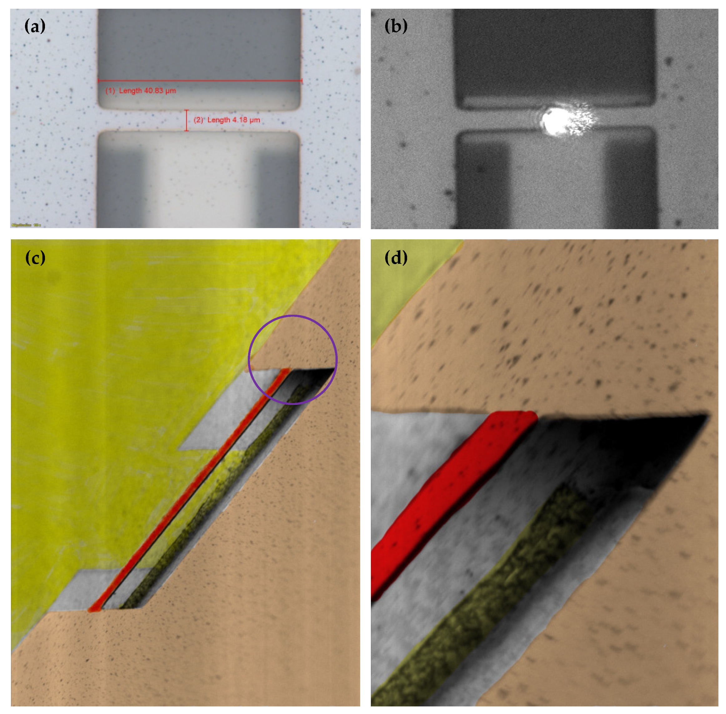
3. Fabrication
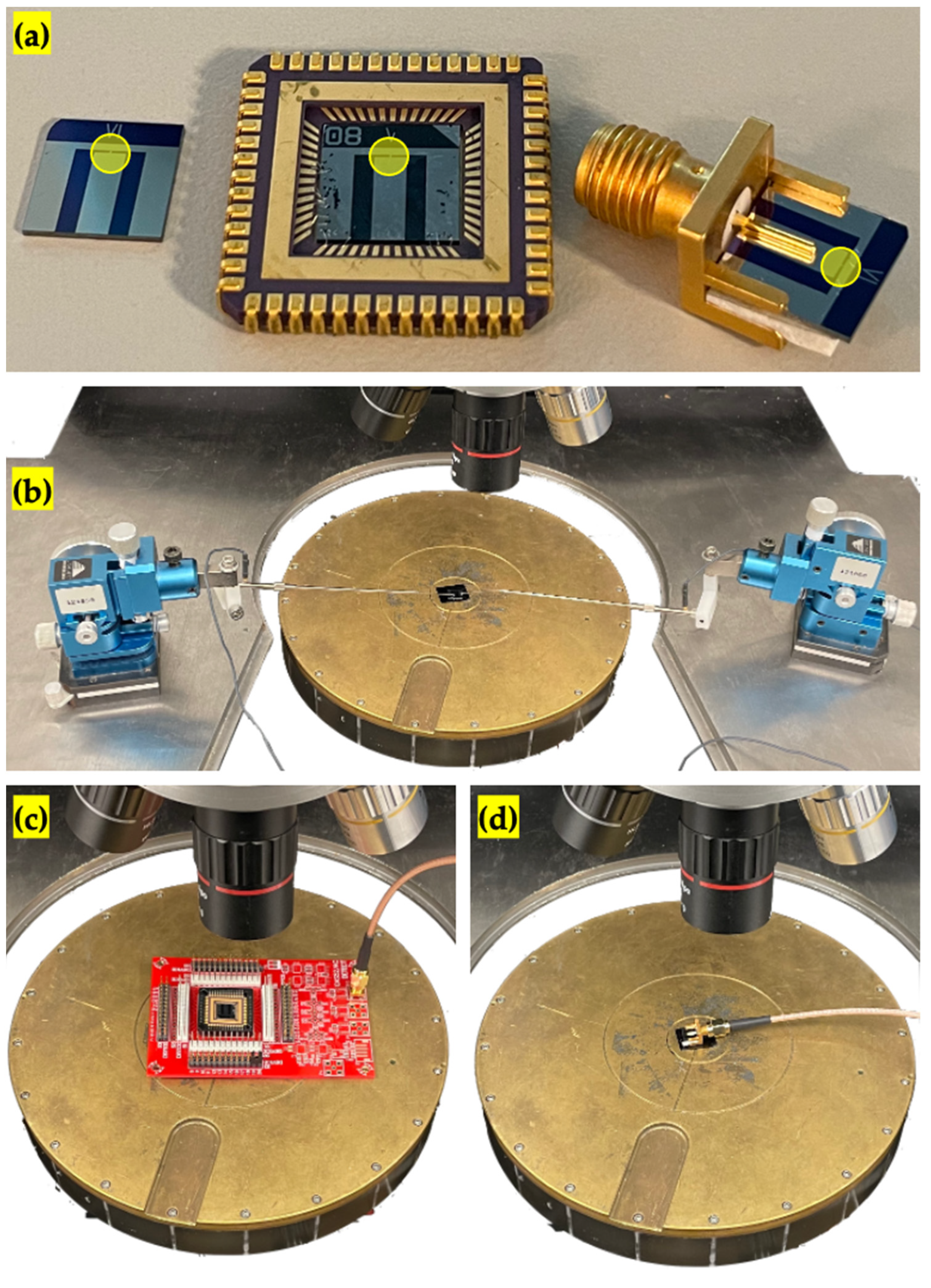
4. Packaging
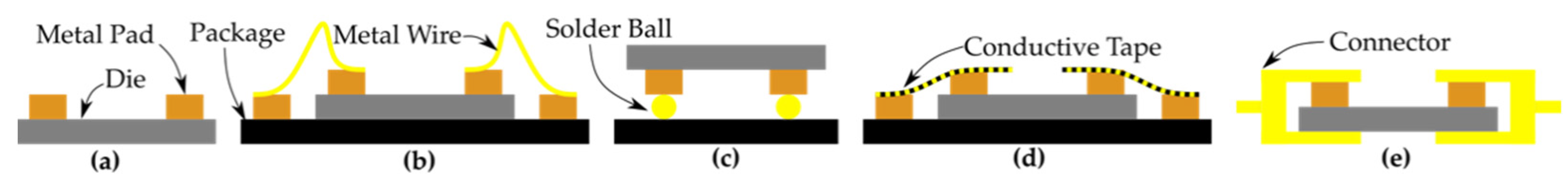
4.1. Wire Bonding
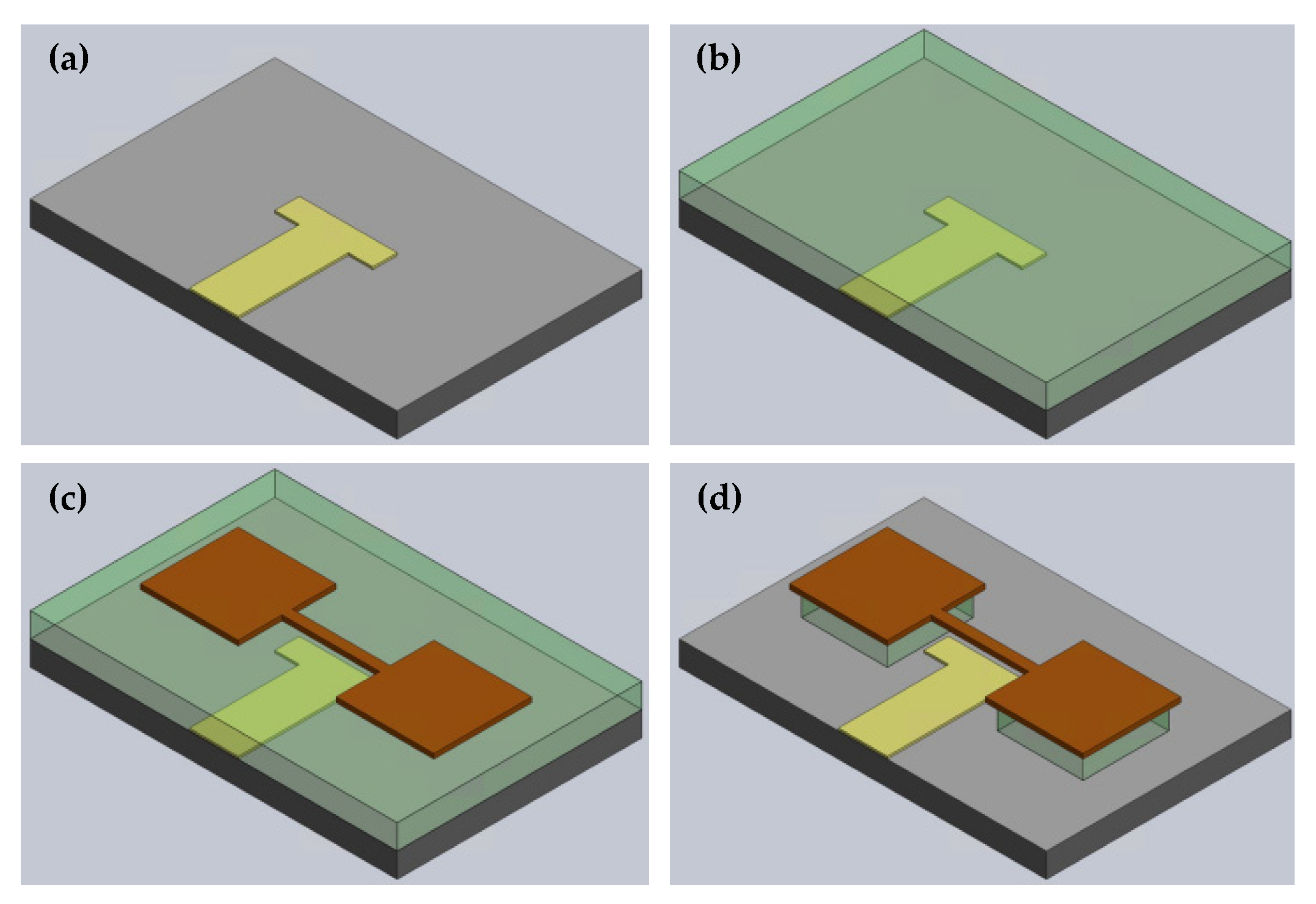
4.2. Built-In
5. Characterization
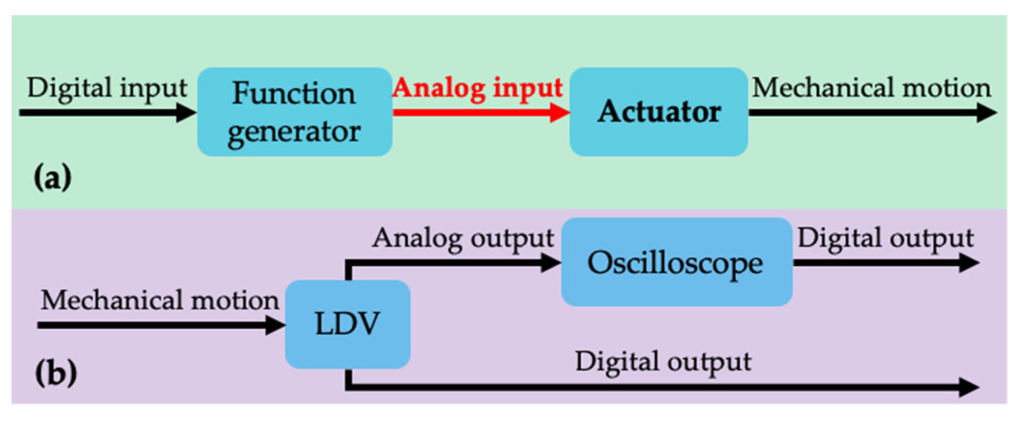
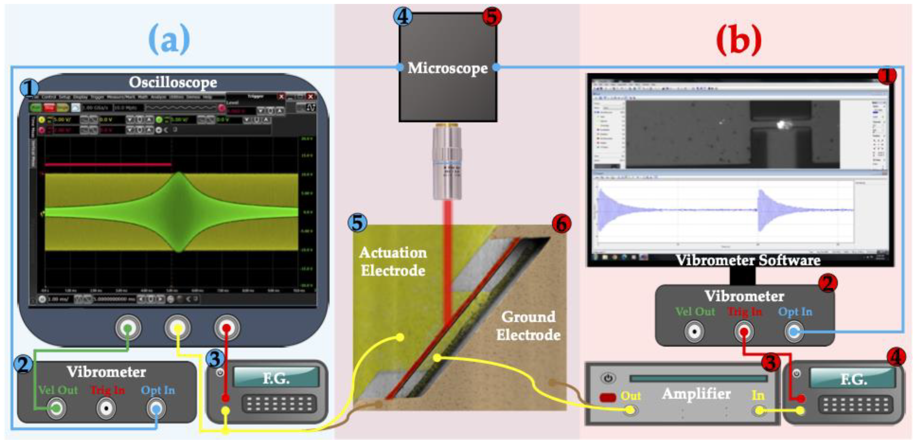
5.1. Purpose
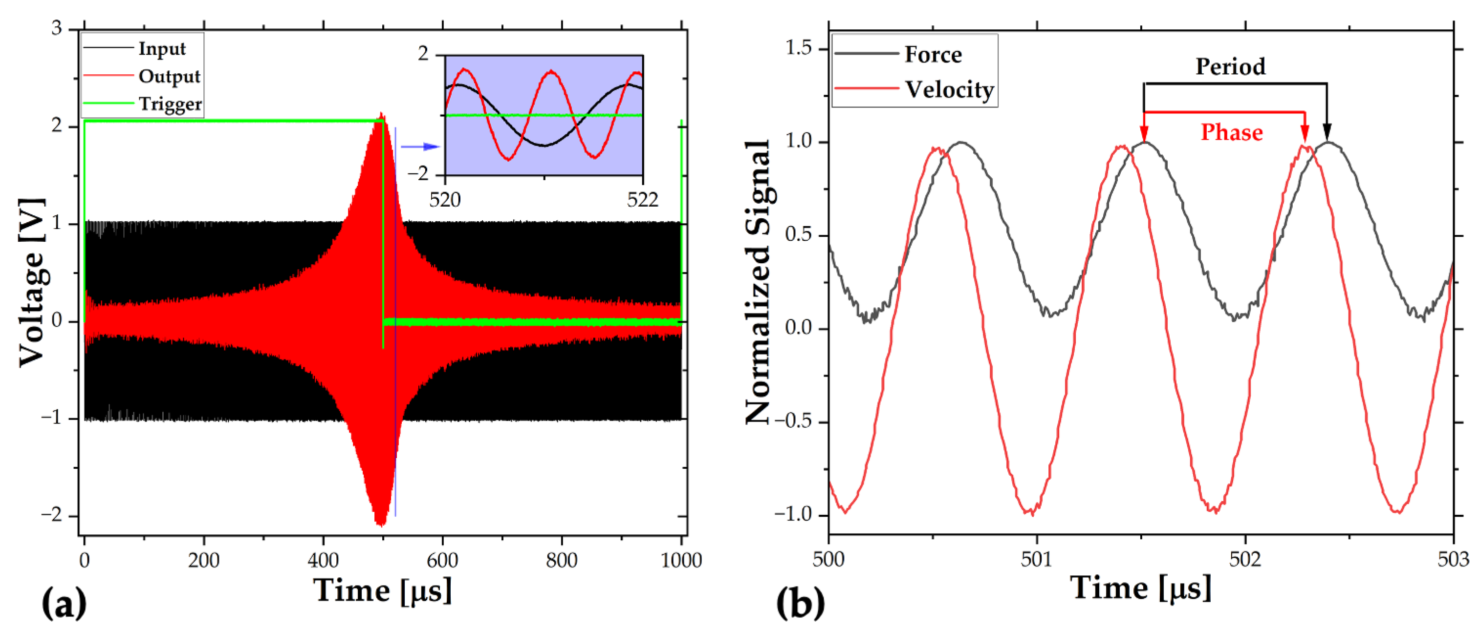
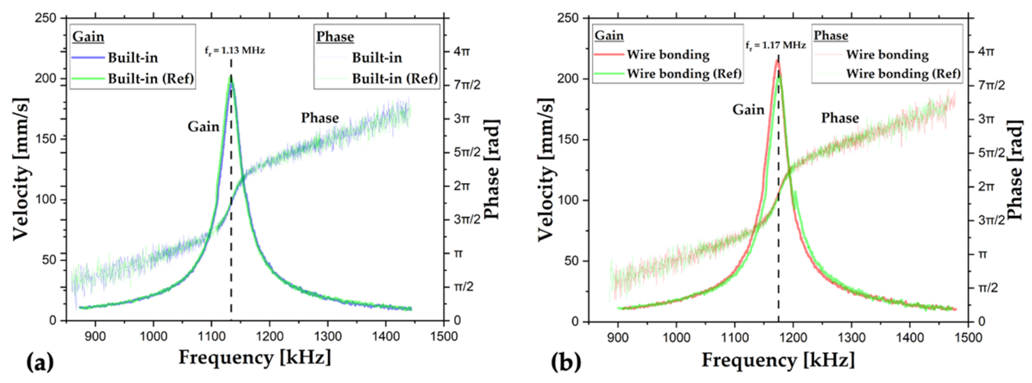
5.2. Frequency Sweep
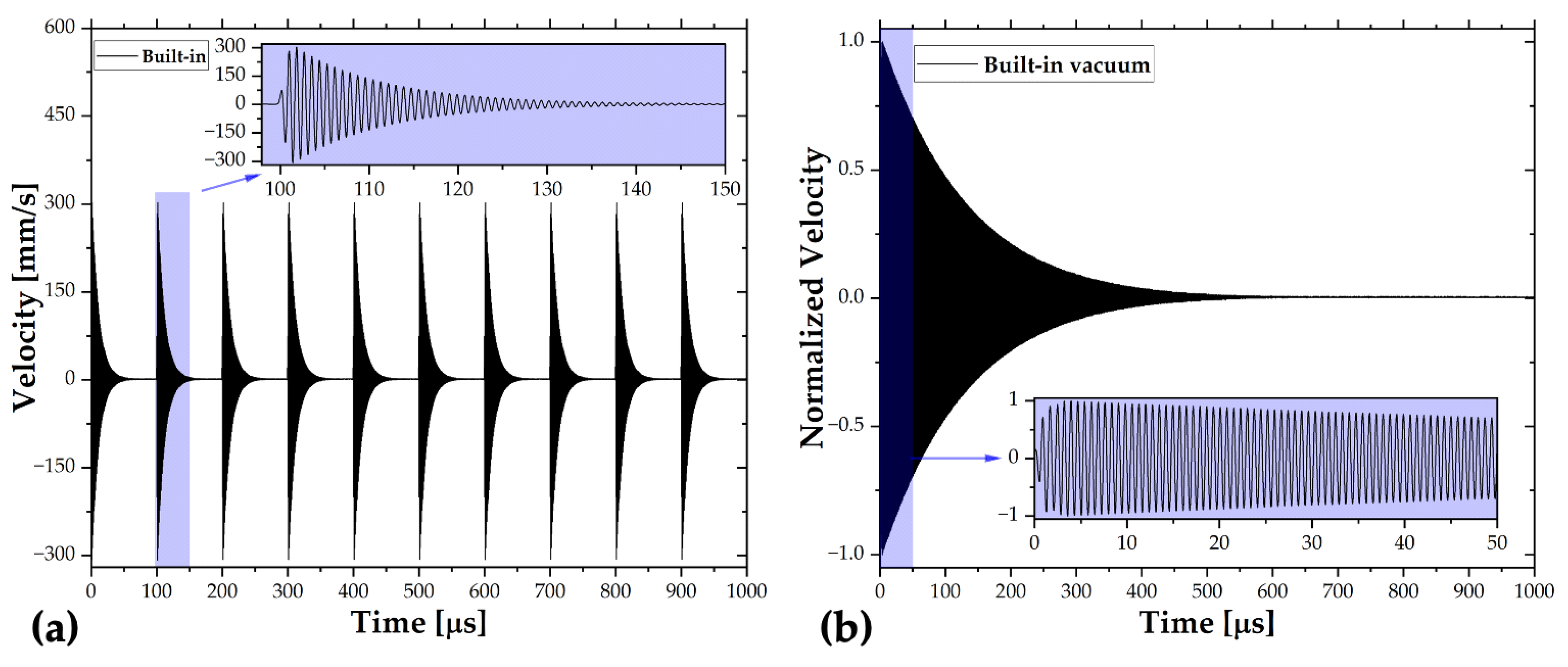
5.3. Pulse Response
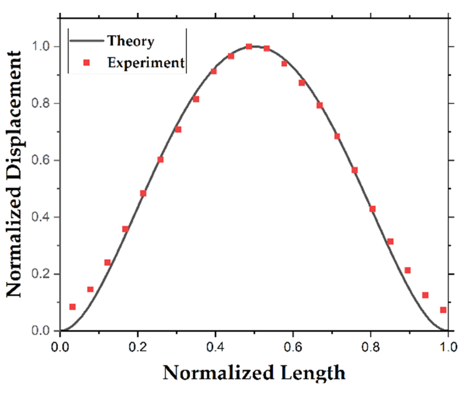
5.4. Mode Shape
6. Results and Discussion
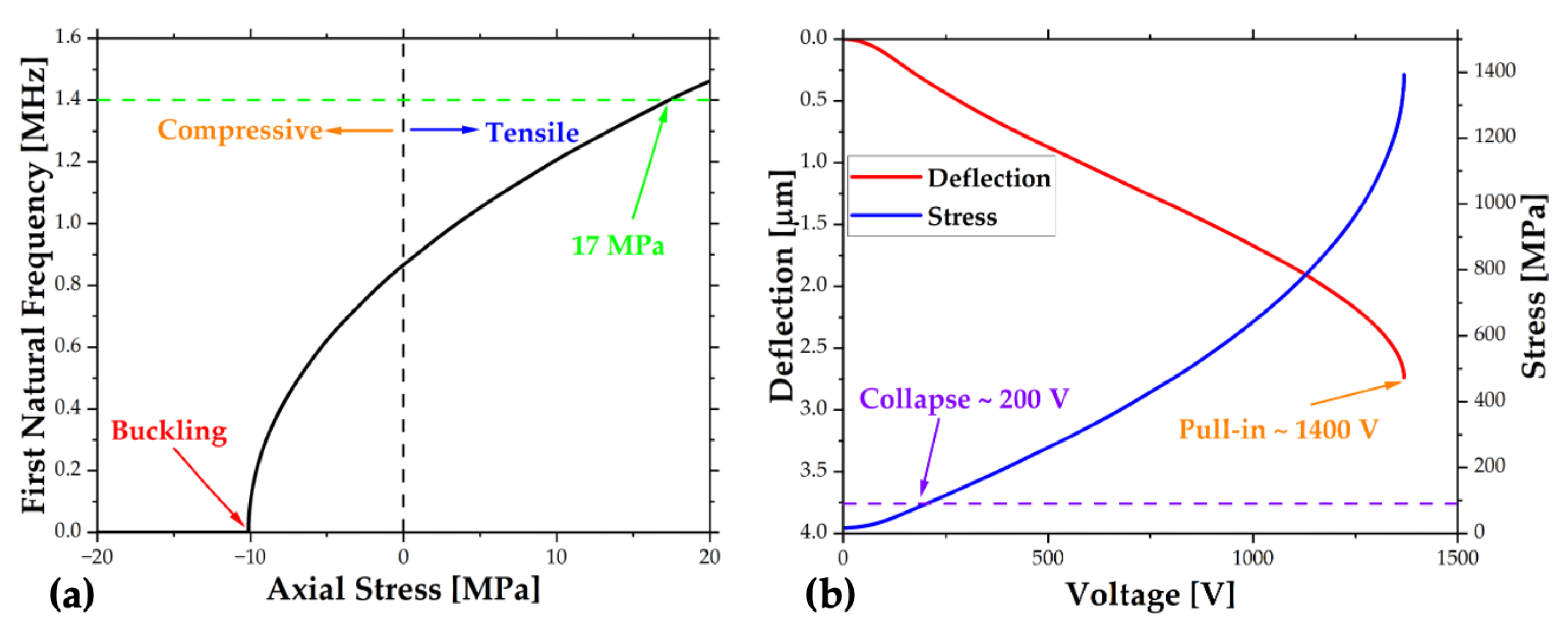
6.1. Frequency Sweep
6.2. Pulse Response
6.3. Mode Shape
7. Conclusions
Supplementary Materials
Author Contributions
Funding
Institutional Review Board Statement
Informed Consent Statement
Data Availability Statement
Acknowledgments
Conflicts of Interest
References
- Xu, J.; Bertke, M.; Li, X.; Mu, H.; Zhou, H.; Yu, F.; Hamdana, G.; Schmidt, A.; Bremers, H.; Peiner, E. Fabrication of ZnO nanorods and Chitosan@ZnO nanorods on MEMS piezoresistive self-actuating silicon microcantilever for humidity sensing. Sens. Actuators B Chem. 2018, 273, 276–287. [Google Scholar] [CrossRef]
- Rahmanian, S.; Hosseini-Hashemi, S.; Rezaei, M. Out-of-plane motion detection in encapsulated electrostatic MEMS gyroscopes: Principal parametric resonance. Int. J. Mech. Sci. 2021, 190, 106022. [Google Scholar] [CrossRef]
- Moudgil, A.; Singh, S.; Mishra, N.; Mishra, P.; Das, S. MoS2/TiO2 Hybrid Nanostructure-Based Field-Effect Transistor for Highly Sensitive, Selective, and Rapid Detection of Gram-Positive Bacteria. Adv. Mater. Technol. 2020, 5, 1900615. [Google Scholar] [CrossRef]
- Geng, Q.; Wang, D.; Chen, P.; Chen, S.C. Ultrafast multi-focus 3-D nano-fabrication based on two-photon polymerization. Nat. Commun. 2019, 10, 2179. [Google Scholar] [CrossRef] [PubMed]
- van Wees, B.J.; van Houten, H.; Beenakker, C.W.J.; Williamson, J.G.; Kouwenhoven, L.P.; van der Marel, D.; Foxon, C.T. Quantized Conductance of Point Contacts in a Two-Dimensional Electron Gas. Phys. Rev. Lett. 1988, 60, 848. [Google Scholar] [CrossRef] [Green Version]
- Chatrchyan, S. Observation of a new boson at a mass of 125 GeV with the CMS experiment at the LHC. Phys. Lett. B 2012, 716, 30–61. [Google Scholar] [CrossRef]
- Chaste, J.; Eichler, A.; Moser, J.; Ceballos, G.; Rurali, R.; Bachtold, A. A nanomechanical mass sensor with yoctogram resolution. Nat. Nanotechnol. 2012, 7, 301–304. [Google Scholar] [CrossRef]
- Komiyama, S.; Astafiev, O.; Antonov23, V.; Kutsuwa, T.; Hirai, H. A single-photon detector in the far-infrared range. Nature 2000, 403, 405–407. Available online: www.nature.com (accessed on 1 May 2022). [CrossRef]
- Park, S.; Abdel-Rahman, E. Low Voltage Electrostatic Actuation and Displacement Measurement through Resonant Drive Circuit. Int. Des. Eng. Tech. Conf. Comput. Inf. Eng. Conf. 2012, 45042, 119–126. Available online: http://asmedigitalcollection.asme.org/IDETC-CIE/proceedings-pdf/IDETC-CIE2012/45042/119/4254395/119_1.pdf (accessed on 1 May 2022).
- Setiono, A.; Fahrbach, M.; Deutschinger, A.; Fantner, E.J.; Schwalb, C.H.; Syamsu, I.; Wasisto, H.S.; Peiner, E. Performance of an electrothermal mems cantilever resonator with fano-resonance annoyance under cigarette smoke exposure. Sensors 2021, 21, 4088. [Google Scholar] [CrossRef]
- Xu, Y.; Lee, J.E.Y. Single-device and on-chip feedthrough cancellation for hybrid MEMS resonators. IEEE Trans. Ind. Electron. 2012, 59, 4930–4937. [Google Scholar] [CrossRef]
- Kassie, D.A.; Elata, D. Harmonic biasing in a double-sided comb-drive resonator, for resolving feed-through issues in low-power driving. Sens. Actuators A Phys. 2021, 332, 113031. [Google Scholar] [CrossRef]
- Mahajan, R.; Qian, Z.; Viswanath, R.S.; Srinivasan, S.; Aygun, K.; Jen, W.L.; Sharan, S.; Dhall, A. Embedded Multidie Interconnect Bridge—A Localized, High-Density Multichip Packaging Interconnect. IEEE Trans. Compon. Packag. Manuf. Technol. 2019, 9, 1952–1962. [Google Scholar] [CrossRef]
- Saleem, M.M.; Saghir, S.; Bukhari, S.A.R.; Hamza, A.; Shakoor, R.I.; Bazaz, S.A. A low-g MEMS accelerometer with high sensitivity, low nonlinearity and large dynamic range based on mode-localization of 3-dofweakly coupled resonators. Micromachines 2021, 12, 310. [Google Scholar] [CrossRef] [PubMed]
- Askari, S.; Asadian, M.H.; Shkel, A.M. Performance of quad mass gyroscope in the angular rate mode. Micromachines 2021, 12, 266. [Google Scholar] [CrossRef] [PubMed]
- Meesala, V.C.; Hajj, M.R.; Abdel-Rahman, E. Bifurcation-based MEMS mass sensors. Int. J. Mech. Sci. 2020, 180, 105705. [Google Scholar] [CrossRef]
- Mistry, K.; Nguyen, V.H.; Arabi, M.; Ibrahim, K.H.; Asgarimoghaddam, H.; Yavuz, M.; Muñoz-Rojas, D.; Abdel-Rahman, E.; Musselman, K.P. Highly Sensitive Self-Actuated Zinc Oxide Resonant Microcantilever Humidity Sensor. Nano Lett. 2022, 22, 3196–3203. [Google Scholar] [CrossRef]
- Cai, C.; Tan, J.; Hua, D.; Qin, M.; Zhu, N. Piezoresistive temperature sensors fabricated by a surface micromachining CMOS MEMS process. Sci. Rep. 2018, 8, 17065. [Google Scholar] [CrossRef] [Green Version]
- Hasan, M.H.; Alsaleem, F.M.; Ouakad, H.M. Novel threshold pressure sensors based on nonlinear dynamics of MEMS resonators. J. Micromech. Microeng. 2018, 28, 065007. [Google Scholar] [CrossRef]
- Al-Ghamdi, M.S.; Khater, M.E.; Stewart, K.M.E.; Alneamy, A.; Abdel-Rahman, E.M.; Penlidis, A. Dynamic bifurcation MEMS gas sensors. J. Micromech. Microeng. 2019, 29, 015005. [Google Scholar] [CrossRef]
- IEEE Electron Devices Society; Institute of Electrical and Electronics Engineers. In Proceedings of the 2019 20th International Conference on Solid-State Sensors, Actuators and Microsystems & Eurosensors XXXIII (TRANSDUCERS & EUROSENSORS XXXIII), Berlin, Germany, 23–27 June 2019. Available online: https://ieeexplore.ieee.org/xpl/conhome/8787960/proceeding (accessed on 1 May 2022).
- Mbarek, S.B.; Alcheikh, N.; Ouakad, H.M.; Younis, M.I. Highly sensitive low field Lorentz-force MEMS magnetometer. Sci. Rep. 2021, 11, 21634. [Google Scholar] [CrossRef] [PubMed]
- Chen, K.; Gong, Z.; Yu, Q. Fiber-amplifier-enhanced resonant photoacoustic sensor for sub-ppb level acetylene detection. Sens. Actuators A Phys. 2018, 274, 184–188. [Google Scholar] [CrossRef]
- Novodchuk, I.; Kayaharman, M.; Prassas, I.; Soosaipillai, A.; Karimi, R.; Goldthorpe, I.A.; Abdel-Rahman, E.; Sanderson, J.; Diamandis, E.P.; Bajcsy, M.; et al. Electronic field effect detection of SARS-CoV-2 N-protein before the onset of symptoms. Biosens. Bioelectron. 2022, 210, 114331. [Google Scholar] [CrossRef] [PubMed]
- Elhady, A.; Abdel-Rahman, E. Measurement of the electric permittivity using Bleustein–Gulyaev wave sensor. J. Micromech. Microeng. 2022, 32. [Google Scholar] [CrossRef]
- Kocer, S.; Mukhangaliyeva, L.; Saritas, R.; Gulsaran, A.; Elhady, A.; Bell, K.; Kamel, A.; Basha, M.; Das, T.; Kayaharman, M.; et al. Resonant Varifocal Mems Mirror. In Proceedings of the 2022 IEEE 35th International Conference on Micro Electro Mechanical Systems Conference (MEMS), Tokyo, Japan, 9–13 January 2022. [Google Scholar]
- Yang, H.; Cheng, Q.; Chen, R.; Bergman, K. Polarization-Diversity Microring-Based Optical Switch Fabric in a Switch-and-Select Architecture. In Proceedings of the 2020 Optical Fiber Communications Conference and Exhibition (OFC), San Diego, CA, USA, 8–12 March 2020. [Google Scholar]
- Zhang, X.; Kwon, K.; Henriksson, J.; Luo, J.; Wu, M.C. A large-scale microelectromechanical-systems-based silicon photonics LiDAR. Nature 2022, 603, 253–258. [Google Scholar] [CrossRef]
- Chaintoutis, C.; Shariati, B.; Bogris, A.; Dijk, P.v.; Roeloffzen, C.G.H.; Bourderionnet, J.; Tomkos, I.; Syvridis, D. Free space intra-datacenter interconnects based on 2D optical beam steering enabled by photonic integrated circuits. Photonics 2018, 5, 21. [Google Scholar] [CrossRef] [Green Version]
- Kokkoniemi, R.; Girard, J.P.; Hazra, D.; Laitinen, A.; Govenius, J.; Lake, R.E.; Sallinen, I.; Vesterinen, V.; Partanen, M.; Tan, J.Y.; et al. Bolometer operating at the threshold for circuit quantum electrodynamics. Nature 2020, 586, 47–51. [Google Scholar] [CrossRef]
- Luo, W.; Weng, Q.; Long, M.; Wang, P.; Gong, F.; Fang, H.; Luo, M.; Wang, W.; Wang, Z.; Zheng, D.; et al. Room-Temperature Single-Photon Detector Based on Single Nanowire. Nano Letters 2018, 18, 5439–5445. [Google Scholar] [CrossRef]
- Azer, B.B.; Gulsaran, A.; Pennings, J.R.; Saritas, R.; Kocer, S.; Bennett, J.L.; Abhang, Y.D.; Pope, M.A.; Abdel-Rahman, E.; Yavuz, M. A Review: TiO2 based photoelectrocatalytic chemical oxygen demand sensors and their usage in industrial applications. J. Electroanal. Chem. 2022, 918, 116466. [Google Scholar] [CrossRef]
- Alshehri, A.H.; Mistry, K.; Nguyen, V.H.; Ibrahim, K.H.; Muñoz-Rojas, D.; Yavuz, M.; Musselman, K.P. Quantum-Tunneling Metal-Insulator-Metal Diodes Made by Rapid Atmospheric Pressure Chemical Vapor Deposition. Adv. Funct. Mater. 2019, 29, 1805533. [Google Scholar] [CrossRef]
- Ivanov, T.G.; Weil, J.; Shah, P.B.; Birdwell, A.G.; Kingkeo, K.; Viveiros, E.A. Diamond RF Transistor Technology with ft=41 GHz and fmax=44 GHz. In Proceedings of the 2018 IEEE/MTT-S International Microwave Symposium–IMS, Philadelphia, PA, USA, 10–15 June 2018; pp. 1461–1463. [Google Scholar] [CrossRef]
- Hedayati, M.K.; Abdipour, A.; Shirazi, R.S.; Ammann, M.J.; John, M.; Cetintepe, C.; Staszewski, R.B. Challenges in On-Chip Antenna Design and Integration with RF Receiver Front-End Circuitry in Nanoscale CMOS for 5G Communication Systems. IEEE Access 2019, 7, 43190–43204. [Google Scholar] [CrossRef]
- Xu, Y.; Tian, Y.; Zhang, B.; Duan, J.; Yan, L. A novel RF MEMS switch on frequency reconfigurable antenna application. Microsyst. Technol. 2018, 24, 3833–3841. [Google Scholar] [CrossRef]
- Singh, T.; Khaira, N.K.; Mansour, R.R. Thermally Actuated SOI RF MEMS-Based Fully Integrated Passive Reflective-Type Analog Phase Shifter for mmWave Applications. IEEE Trans. Microw. Theory Tech. 2021, 69, 119–131. [Google Scholar] [CrossRef]
- Song, P.; Hashemi, H. RF Filter Synthesis Based on Passively Coupled N-Path Resonators. IEEE J. Solid-State Circuits 2019, 54, 2475–2486. [Google Scholar] [CrossRef]
- Ranjbar, E.; Yaghoubi, M.; Suratgar, A.A. Adaptive Sliding Mode Controller Design for a Tunable Capacitor Susceptible to Unknown Upper-Bounded Uncertainties and Disturbance. Iran. J. Sci. Technol. Trans. Electr. Eng. 2020, 44, 327–346. [Google Scholar] [CrossRef]
- Mi, S.; Pu, H.; Xia, S.; Sun, W. A Minimized Valveless Electromagnetic Micropump for Microfluidic Actuation on Organ Chips. Sens. Actuators A Phys. 2020, 301, 111704. [Google Scholar] [CrossRef]
- Shan, L.; Cui, M.; Meacham, J.M. Spray characteristics of an ultrasonic microdroplet generator with a continuously variable operating frequency. J. Acoust. Soc. Am. 2021, 150, 1300–1310. [Google Scholar] [CrossRef]
- Li, M.; Li, D. Microvalve using electrokinetic motion of electrically induced Janus droplet. Anal. Chim. Acta 2018, 1021, 85–94. [Google Scholar] [CrossRef]
- Khan, A.A.; Saritas, R.; Rana, M.M.; Tanguy, N.; Zhu, W.; Mei, N.; Kokilathasan, S.; Rassel, S.; Leonenko, Z.; Yan, N.; et al. Performance-Improved Highly Integrated Uniaxial Tristate Hybrid Nanogenerator for Sustainable Mechanical Energy Harvesting. ACS Appl. Mater. Interfaces 2022, 14, 4119–4131. [Google Scholar] [CrossRef]
- Aldrigo, M.; Dragoman, M.; Modreanu, M.; Povey, I.; Iordanescu, S.; Vasilache, D.; Dinescu, A.; Shanawani, M.; Masotti, D. Harvesting Electromagnetic Energy in the V -Band Using a Rectenna Formed by a Bow Tie Integrated with a 6-nm-Thick Au/HfO2/Pt Metal-Insulator-Metal Diode. IEEE Trans. Electron Devices 2018, 65, 2973–2980. [Google Scholar] [CrossRef]
- Alneamy, A.M.; Khater, M.E.; Abdel-Aziz, A.K.; Heppler, G.R.; Abdel-Rahman, E.M. Electrostatic arch micro-tweezers. Int. J. Non-Linear Mech. 2020, 118, 103298. [Google Scholar] [CrossRef]
- Arabi, M.; Gopanchuk, M.; Abdel-Rahman, E.; Yavuz, M. Measurement of in-plane motions in MEMS. Sensors 2020, 20, 3594. [Google Scholar] [CrossRef] [PubMed]
- Sheppard, C.J.R. MICROSCOPY Contents Overview Confocal Microscopy Imaging Multiple Photon Fluorescence Microscopy Interference Microscopy Nonlinear Microscopy Phase Contrast Microscopy Overview. Available online: https://www.sciencedirect.com/science/article/pii/B012369395000823X?via%3Dihub (accessed on 1 May 2022). [CrossRef]
- Hagen, E.; Rubens, H. Über Beziehungen des Reflexions-und Emissionsvermögens der Metalle zu ihrem elektrischen Leitvermögen. Ann. Der Phys. 1903, 316, 873–901. [Google Scholar] [CrossRef] [Green Version]
- Abdel-Rahman, E.M.; Mohammad, I.Y.; Ali, H.N. Characterization of the mechanical behavior of an electrically actuated microbeam. J. Micromechan. Microeng. 2002, 12, 759. [Google Scholar] [CrossRef]
- Lu, Q.; Fang, W.; Wang, C.; Bai, J.; Yao, Y.; Chen, J.; Xu, X.; Huang, W. Investigation of a complete squeeze-film damping model for MEMS devices. Microsyst. Nanoeng. 2021, 7, 1–13. [Google Scholar] [CrossRef]
- Ghosh, A. Scaling Laws. In Mechanics over Micro and Nano Scales; Chakraborty, S., Ed.; Springer: New York, NY, USA, 2011. [Google Scholar] [CrossRef]
- Okazaki, S. Resolution limits of optical lithography. J. Vac. Sci. Technol. B Microelectron. Nanometer Struct. 1991, 9, 2829. [Google Scholar] [CrossRef]
- Bartek, M.; Wolffenbuttel, R.F. Dry release of metal structures in oxygen plasma: Process characterization and optimization. J. Micromech. Microeng. 1998, 8, 91. [Google Scholar] [CrossRef]
- AC/DC Module User’s Guide. Available online: www.comsol.com/blogs (accessed on 1 May 2022).
- Structural Mechanics Module User’s Guide. Available online: www.comsol.com/blogs (accessed on 1 May 2022).
- Hachette Pratique., Macrolibros), Les carrés d’Art Thérapie Winnie L’ourson: [Album à colorier]. Hachette Livre-Département Pratique. 2018. Available online: https://www.wiley.com/en-us/Materials+Science+and+Engineering%3A+An+Introduction%2C+10th+Edition-p-9781119405498 (accessed on 1 May 2022).
- Thornton, J.A. Influence of substrate temperature and deposition rate on structure of thick sputtered Cu coatings. J. Vac. Sci. Technol. 1975, 12, 830–835. [Google Scholar] [CrossRef]
- Chason, E.; Guduru, P.R. Tutorial: Understanding residual stress in polycrystalline thin films through real-time measurements and physical models. J. Appl. Phys. 2016, 119, 191101. [Google Scholar] [CrossRef]
- Hull, R.; Bean, J.C. Misfit Dislocations in Lattice-Mismatched Epitaxial Films. Crit. Rev. Solid State Mater. Sci. 1992, 17, 507–546. [Google Scholar] [CrossRef]
- Seel, S.C.; Thompson, C.V. Tensile stress generation during island coalescence for variable island-substrate contact angle. J. Appl. Phys. 2003, 93, 9038–9042. [Google Scholar] [CrossRef]
- Korhonen, M.A.; Paszkiet, C.A. X-ray Determination of the Residual Stresses in Thin Aluminum Films Deposited on Silicon Substrates. Scr. Metall. 1989, 23, 1449–1453. [Google Scholar] [CrossRef]
- Paviot, V.M.; Vlassak, J.J.; Nix, W.D. Measuring the Mechanical Properties of Thin Metal Films by Means of Bulge Testing of Micromachined Windows. MRS Online Proc. Libr. (OPL) 1994, 356, 579–584. [Google Scholar] [CrossRef]
- Floro, J.A.; Hearne, S.J.; Hunter, J.A.; Kotula, P.; Chason, E.; Seel, S.C.; Thompson, C.v. The dynamic competition between stress generation and relaxation mechanisms during coalescence of Volmer–Weber thin films. J. Appl. Phys. 2001, 89, 4886–4897. [Google Scholar] [CrossRef] [Green Version]
- van Spengen, W.M. MEMS reliability from a failure mechanisms perspective. Microelectron. Reliab. 2003, 43, 1049–1060. [Google Scholar] [CrossRef]
- Younis, M.I.; Abdel-Rahman, E.M.; Nayfeh, A. A reduced-order model for electrically actuated microbeam-based MEMS. J. Microelectromech. Syst. 2003, 12, 672–680. [Google Scholar] [CrossRef]
- Nayfeh, A.H.; Younis, M.I.; Abdel-Rahman, E.M. Dynamic pull-in phenomenon in MEMS resonators. Nonlinear Dyn. 2007, 48, 153–163. [Google Scholar] [CrossRef]
- LOR and PMGI Resists for Bi-layer Lift-off Processing. Available online: https://kayakuam.com/wp-content/uploads/2019/09/KAM-LOR-PMGI-Data-Sheet-11719.pdf (accessed on 1 May 2022).


| Layer | Step 1 | Step 2 | Step 3 | Step 4 |
|---|---|---|---|---|
| Actuation electrode | PR coating | Lithography | Metal deposition | Liftoff |
| Sacrificial layer | PR coating | - | - | - |
| Structure | Metal deposition | PR coating | Lithography | Dry etch |
| Dicing and Release | Dicing | Dry etch | - | - |
| Device | |||||
|---|---|---|---|---|---|
| Built-in | 1.13 | 29.8 | 67.0 | 38.0 | 38.0 |
| Built-in (Ref) | 1.13 | 30.0 | 66.9 | 37.8 | 38.0 |
| Wire bonding | 1.17 | 30.1 | 67.4 | 38.9 | 39.6 |
| Wire bonding (Ref) | 1.17 | 28.9 | 67.8 | 40.6 | 39.9 |
| Device | BW [kHz] | ||
|---|---|---|---|
| Built-in | 1.17 | 30.1 | 38.7 |
| Reference | 1.16 | 30.2 | 38.4 |
| Vacuum | 1.36 | 2.58 | 529 |
| Wire bonding | 1.12 | 30.3 | 37.0 |
| Reference | 1.11 | 30.4 | 36.4 |
| Vacuum | 1.23 | 2.82 | 436 |
Publisher’s Note: MDPI stays neutral with regard to jurisdictional claims in published maps and institutional affiliations. |
© 2022 by the authors. Licensee MDPI, Basel, Switzerland. This article is an open access article distributed under the terms and conditions of the Creative Commons Attribution (CC BY) license (https://creativecommons.org/licenses/by/4.0/).
Share and Cite
Gulsaran, A.; Bastug Azer, B.; Kocer, S.; Rahmanian, S.; Saritas, R.; Abdel-Rahman, E.M.; Yavuz, M. Built-In Packaging for Single Terminal Devices. Sensors 2022, 22, 5264. https://doi.org/10.3390/s22145264
Gulsaran A, Bastug Azer B, Kocer S, Rahmanian S, Saritas R, Abdel-Rahman EM, Yavuz M. Built-In Packaging for Single Terminal Devices. Sensors. 2022; 22(14):5264. https://doi.org/10.3390/s22145264
Chicago/Turabian StyleGulsaran, Ahmet, Bersu Bastug Azer, Samed Kocer, Sasan Rahmanian, Resul Saritas, Eihab M. Abdel-Rahman, and Mustafa Yavuz. 2022. "Built-In Packaging for Single Terminal Devices" Sensors 22, no. 14: 5264. https://doi.org/10.3390/s22145264
APA StyleGulsaran, A., Bastug Azer, B., Kocer, S., Rahmanian, S., Saritas, R., Abdel-Rahman, E. M., & Yavuz, M. (2022). Built-In Packaging for Single Terminal Devices. Sensors, 22(14), 5264. https://doi.org/10.3390/s22145264