
Pseudo-Static Gain Cell of Embedded DRAM for Processing-in-Memory in Intelligent IoT Sensor Nodes


Abstract
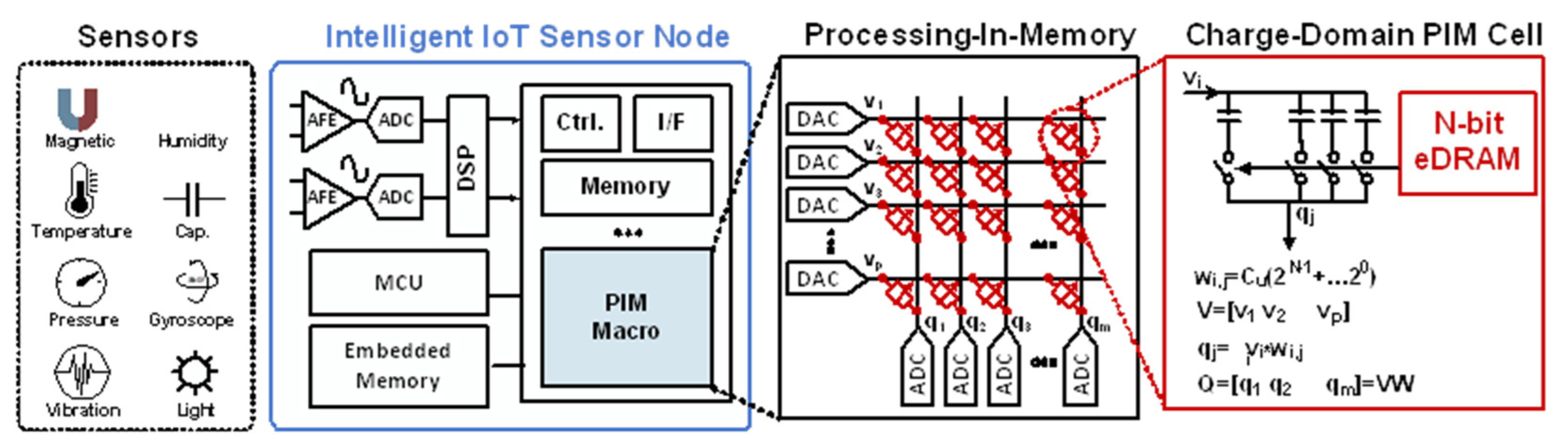
:1. Introduction
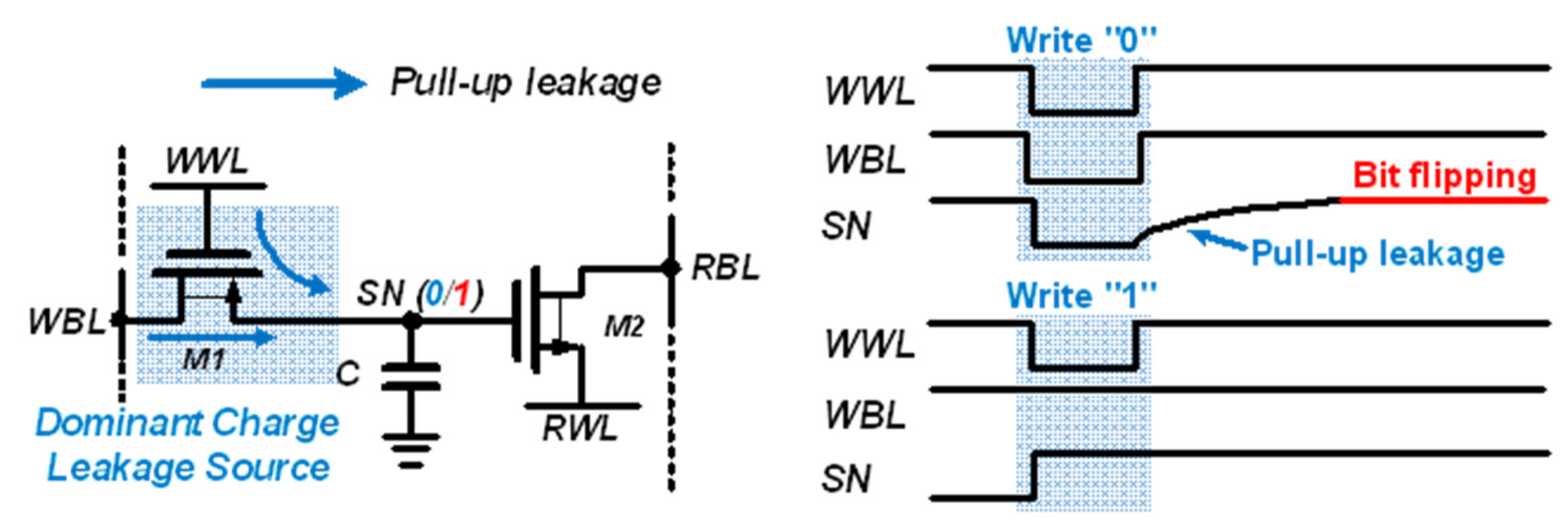
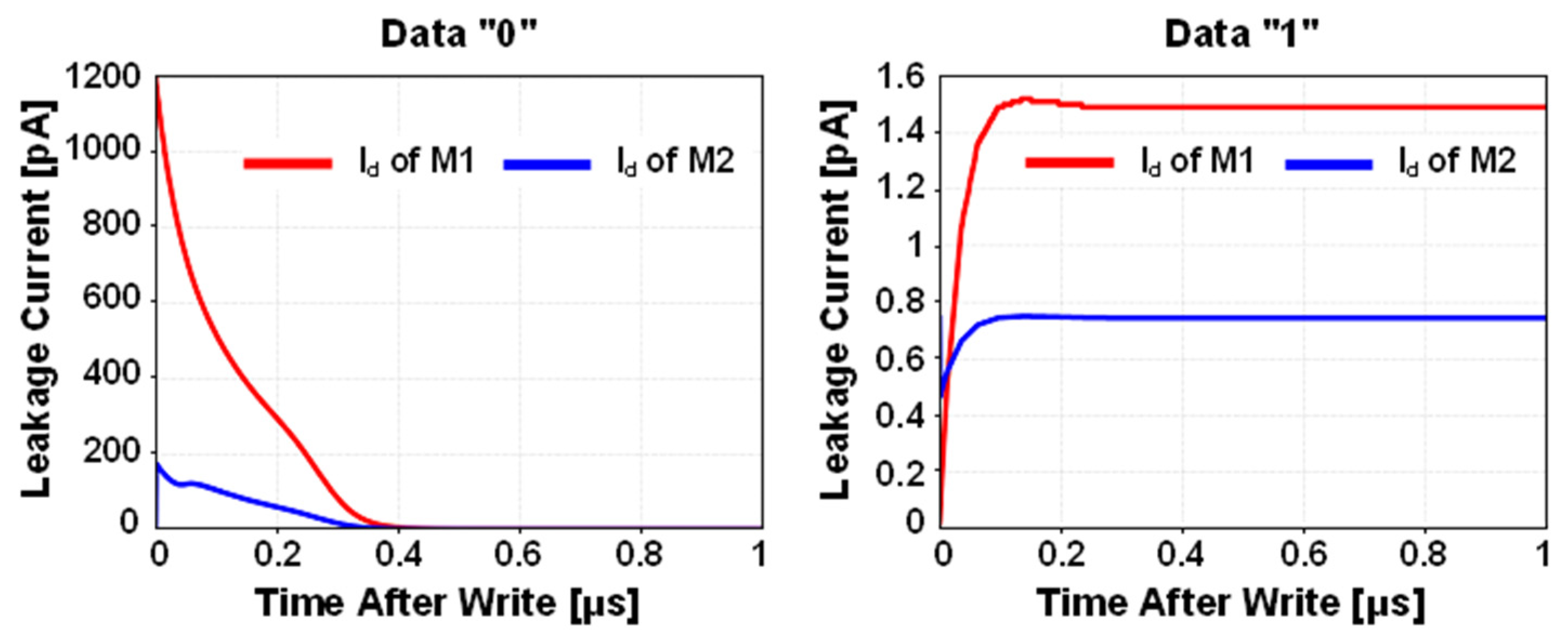
2. Conventional 2T1C Gain Cell and Charge Loss Mechanism
3. Methodology
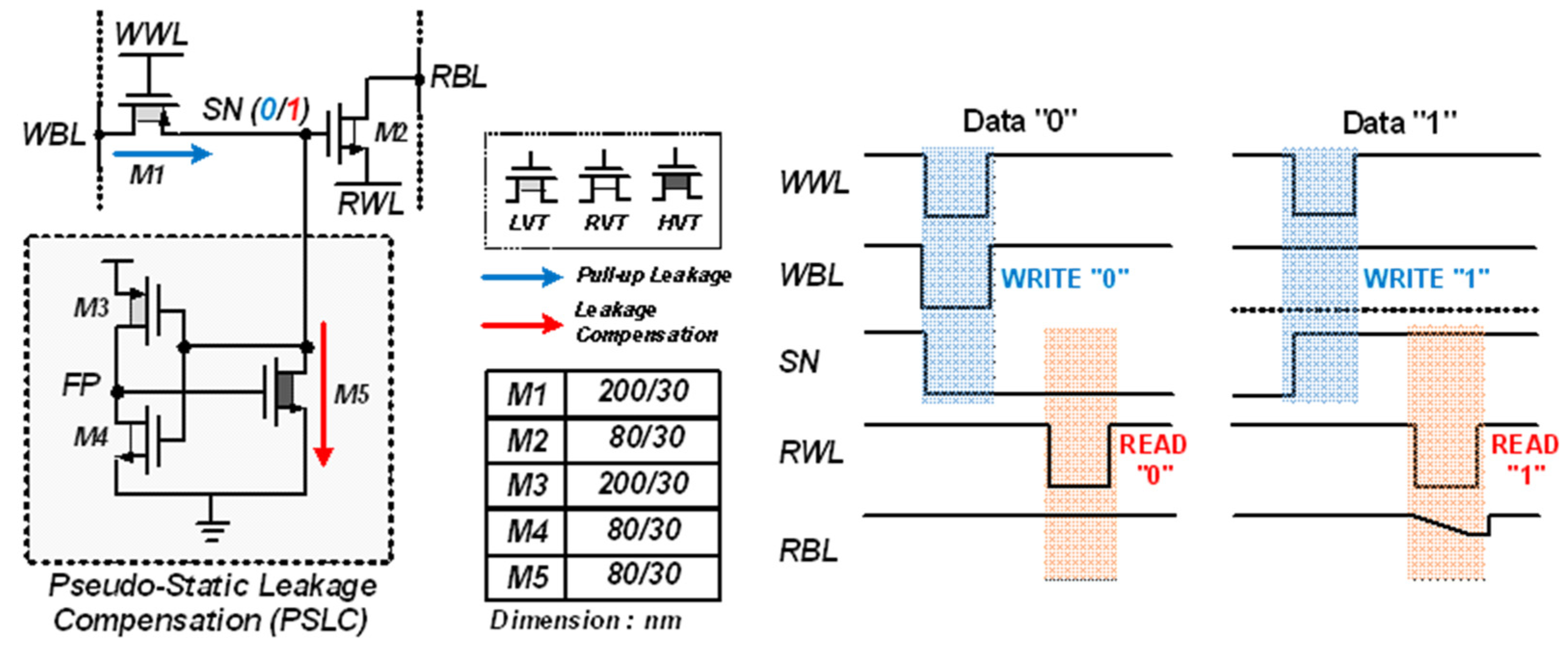
4. Operating Principle and Circuit Implementation of Proposed PS-GC
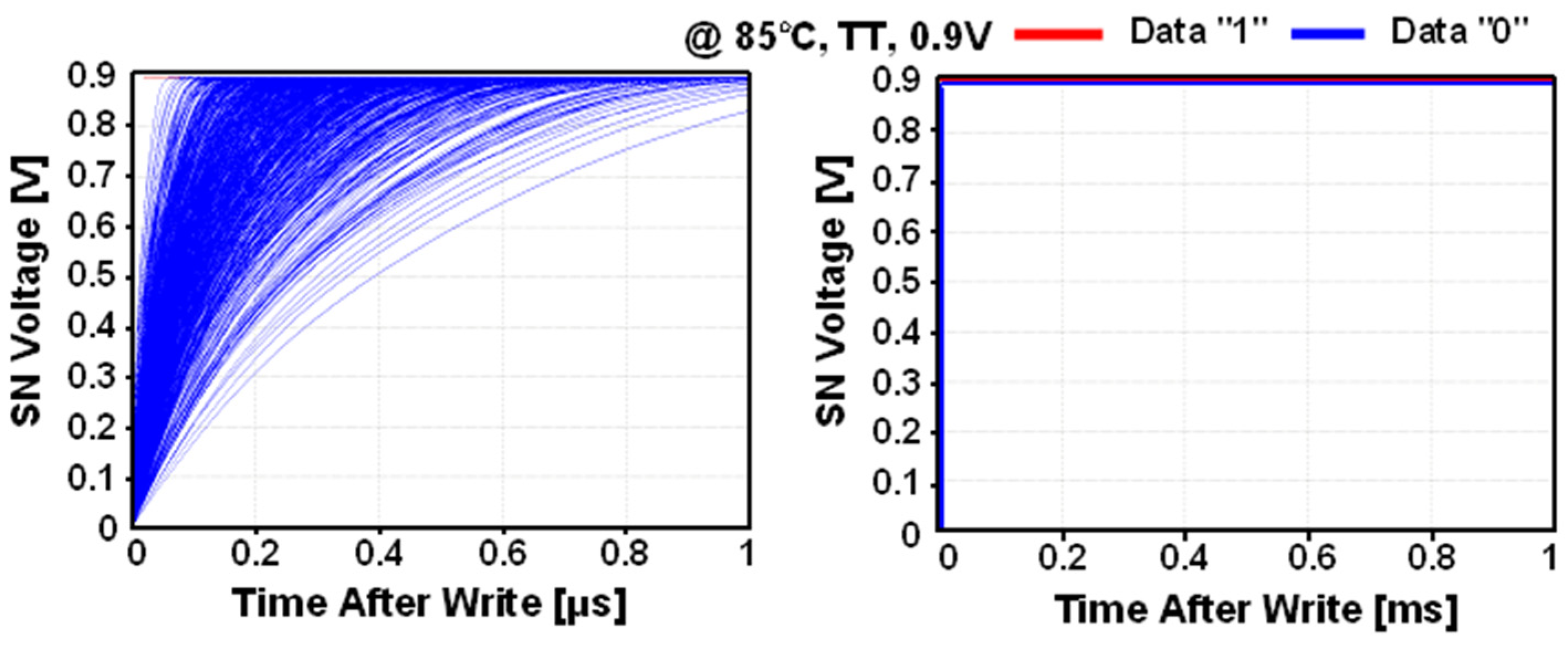
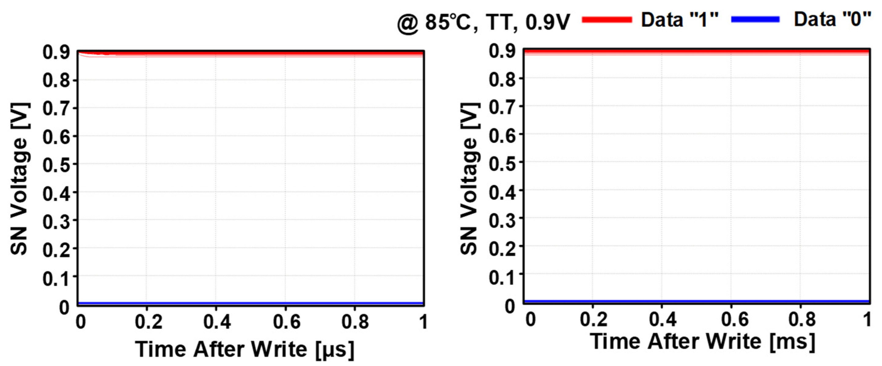
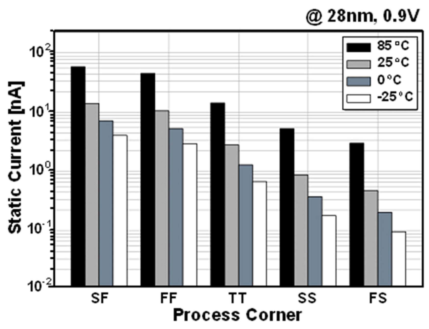
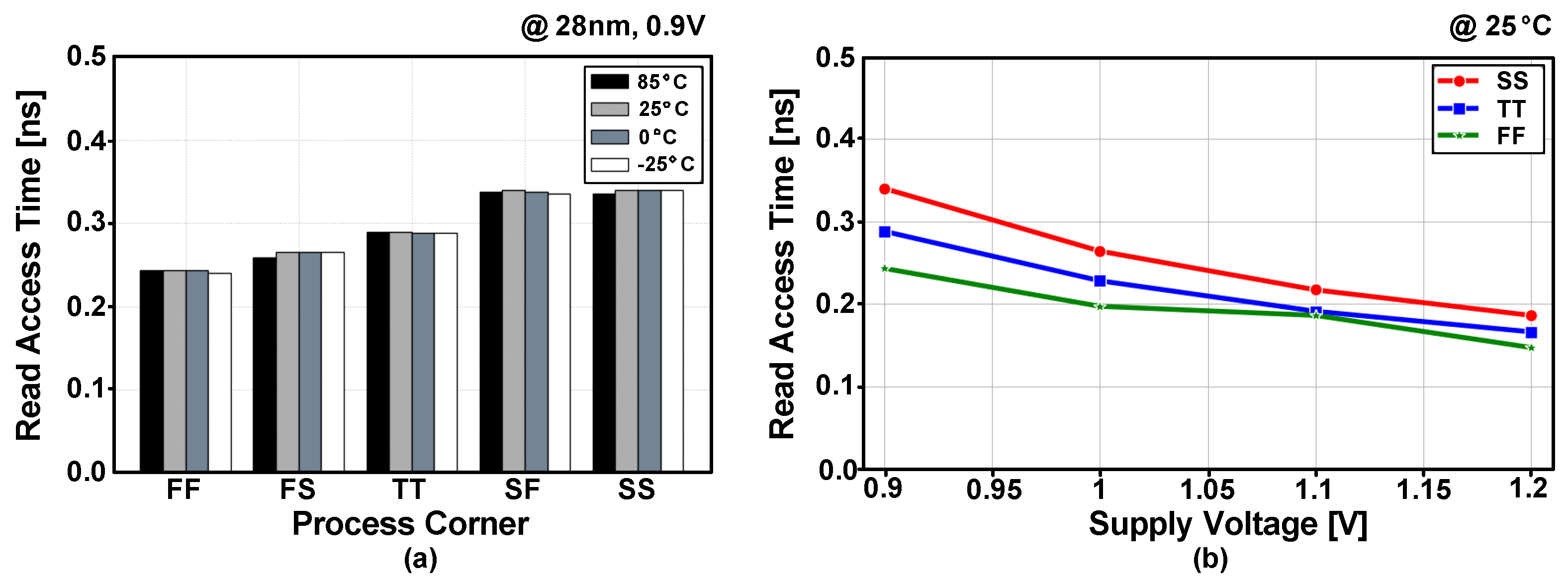
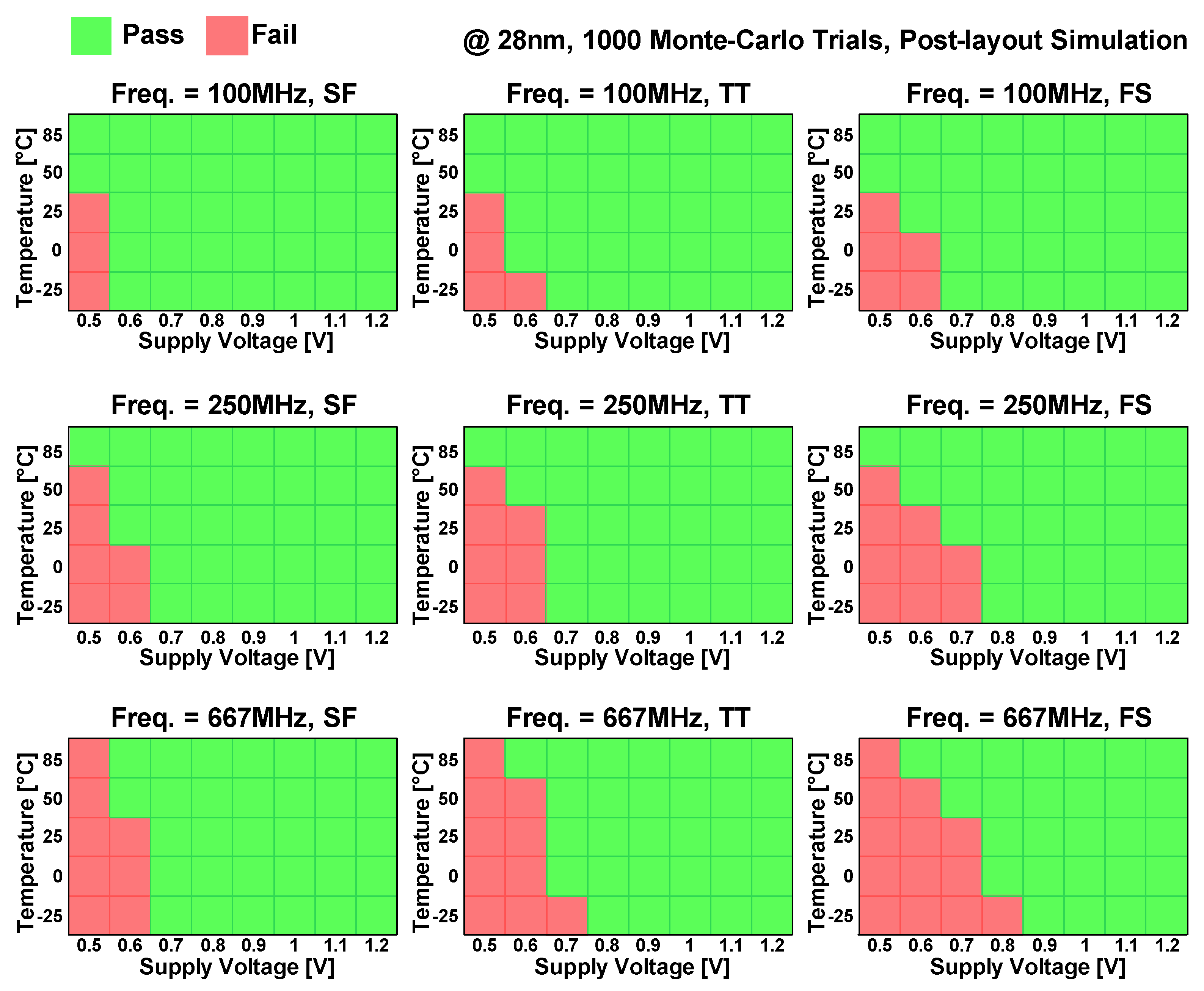
5. Simulation Results and Discussion
6. Conclusions
Author Contributions
Funding
Institutional Review Board Statement
Informed Consent Statement
Data Availability Statement
Conflicts of Interest
References
- Zhang, J.; Wang, Z.; Verma, N. A Machine-learning Classifier Implemented in a Standard 6T SRAM Array. In Proceedings of the IEEE Symposium on VLSI Circuits (VLSI-Circuits), Honolulu, HI, USA, 15–17 June 2016; pp. 1–2. [Google Scholar] [CrossRef]
- Yu, C.; Yoo, T.; Kim, T.T.; Tshun Chuan, K.C.; Kim, B. A 16K Current-Based 8T SRAM Compute-In-Memory Macro with Decoupled Read/Write and 1-5bit Column ADC. In Proceedings of the IEEE Custom Integrated Circuits Conference (CICC), Boston, MA, USA, 22–25 March 2020; pp. 1–4. [Google Scholar] [CrossRef]
- Chae, C.; Kim, S.; Choi, J.; Park, J.-E. A Multi-Bit In-Memory-Computing SRAM Macro Using Column-Wise Charge Redistribution for DNN Inference in Edge Computing Devices. In Proceedings of the 18th International SoC Design Conference (ISOCC), Jeju Island, Korea, 6–9 October 2021; pp. 421–422. [Google Scholar] [CrossRef]
- Jiang, Z.; Yin, S.; Seo, J.; Seok, M. C3SRAM: An In-Memory-Computing SRAM Macro Based on Robust Capacitive Coupling Computing Mechanism. IEEE J. Solid-State Circuits 2020, 55, 1888–1897. [Google Scholar] [CrossRef]
- Chen, Z.; Yu, Z.; Jin, Q.; Wang, J.; Lin, S.; Li, D.; Wang, Y. CAP-RAM: A Charge-Domain In-Memory Computing 6T-SRAM for Accurate and Precision-Programmable CNN Inference. IEEE J. Solid-State Circuits 2021, 56, 1924–1935. [Google Scholar] [CrossRef]
- Biswas, A.; Chandrakasan, A.P. Conv-RAM: An energy-efficient SRAM with embedded convolution computation for low-power CNN-based machine learning applications. In Proceedings of the IEEE International Solid-State Circuits Conference-(ISSCC), San Francisco, CA, USA, 11–15 February 2018; pp. 488–490. [Google Scholar] [CrossRef] [Green Version]
- Su, J.-W.; Chou, Y.-C.; Liu, R.; Liu, T.-W.; Lu, P.-J.; Wu, P.-C.; Chung, Y.-L.; Hung, L.-Y.; Ren, J.-S.; Pan, T.; et al. 16.3 A 28nm 384kb 6T-SRAM Computation-in-Memory Macro with 8b Precision for AI Edge Chips. In Proceedings of the IEEE International Solid-State Circuits Conference (ISSCC), San Francisco, CA, USA, 13–22 February 2021; pp. 250–252. [Google Scholar] [CrossRef]
- Chen, W.-H.; Li, K.-X.; Lin, W.-Y.; Hsu, K.-H.; Li, P.-Y.; Yang, C.-H.; Xue, C.-X.; Yang, E.-Y.; Chen, Y.-K.; Chang, Y.-S.; et al. A 65nm 1Mb nonvolatile computing-in-memory ReRAM macro with sub-16ns multiply-and-accumulate for binary DNN AI edge processors. In Proceedings of the IEEE International Solid-State Circuits Conference-(ISSCC), San Francisco, CA, USA, 11–15 February 2018; pp. 494–496. [Google Scholar] [CrossRef]
- Xue, C.-X.; Chen, W.-H.; Liu, J.-S.; Li, J.-F.; Lin, W.-Y.; Lin, W.-E.; Wang, J.-H.; Wei, W.-C.; Huang, T.-Y.; Chang, T.-W.; et al. Embedded 1-Mb ReRAM-Based Computing-in-Memory Macro with Multibit Input and Weight for CNN-Based AI Edge Processors. IEEE J. Solid-State Circuits 2020, 55, 203–215. [Google Scholar] [CrossRef]
- Khwa, W.-S.; Chiu, Y.-C.; Jhang, C.-J.; Huang, S.-P.; Lee, C.-Y.; Wen, T.-H.; Chang, F.-C.; Yu, S.-M.; Lee, T.-Y.; Chang, M.-F. A 40-nm, 2M-Cell, 8b-Precision, Hybrid SLC-MLC PCM Computing-in-Memory Macro with 20.5-65.0TOPS/W for Tiny-Al Edge Devices. In Proceedings of the IEEE International Solid-State Circuits Conference-(ISSCC), San Francisco, CA, USA, 20–26 February 2022; pp. 1–3. [Google Scholar] [CrossRef]
- Yu, C.; Yoo, T.; Kim, H.; Kim, T.T.-H.; Chuan, K.C.T.; Kim, B. A Logic-Compatible eDRAM Compute-In-Memory with Embedded ADCs for Processing Neural Networks. IEEE Trans. Circuits Syst. I Regul. Pap. 2021, 68, 667–679. [Google Scholar] [CrossRef]
- Xie, S.; Ni, C.; Sayal, A.; Jain, P.; Hamzaoglu, F.; Kulkarni, J.P. 16.2 eDRAM-CIM: Compute-In-Memory Design with Reconfigurable Embedded-Dynamic-Memory Array Realizing Adaptive Data Converters and Charge-Domain Computing. In Proceedings of the IEEE International Solid-State Circuits Conference (ISSCC), San Francisco, CA, USA, 13–22 February 2021; pp. 248–250. [Google Scholar] [CrossRef]
- Raman, S.R.S.; Xie, S.; Kulkarni, J.P. Compute-in-eDRAM with Backend Integrated Indium Gallium Zinc Oxide Transistors. In Proceedings of the IEEE International Symposium on Circuits and Systems (ISCAS), Daegu, Korea, 22–28 May 2021; pp. 1–5. [Google Scholar] [CrossRef]
- Hwang, M.-E.; Kwon, S. A 0.94 μW 611 KHz In-Situ Logic Operation in Embedded DRAM Memory Arrays in 90 nm CMOS. Electronics 2019, 8, 865. [Google Scholar] [CrossRef] [Green Version]
- Schuster, S.E.; Matick, R.E. Fast Low Power eDRAM Hierarchical Differential Sense Amplifier. IEEE J. Solid-State Circuits 2009, 44, 631–641. [Google Scholar] [CrossRef]
- Sudarshan, C.; Steiner, L.; Jung, M.; Lappas, J.; Weis, C.; Wehn, N. A Novel DRAM Architecture for Improved Bandwidth Utilization and Latency Reduction Using Dual-Page Operation. IEEE Trans. Circuits Syst. II Express Briefs 2021, 68, 1615–1619. [Google Scholar] [CrossRef]
- Edri, N.; Meinerzhagen, P.; Teman, A.; Burg, A.; Fish, A. Silicon-Proven, Per-Cell Retention Time Distribution Model for Gain-Cell Based eDRAMs. IEEE Trans. Circuits Syst. I Regul. Pap. 2016, 63, 222–232. [Google Scholar] [CrossRef]
- Golman, R.; Giterman, R.; Teman, A. Configurable Multi-Port Dynamic Bitcell with Internal Refresh Mechanism. In Proceedings of the IEEE International Conference on Electronics, Circuits and Systems (ICECS), Bordeaux, France, 9–12 December 2018; pp. 589–592. [Google Scholar] [CrossRef]
- Maltabashi, O.; Marinberg, H.; Giterman, R.; Teman, A. A 5-Transistor Ternary Gain-Cell eDRAM with Parallel Sensing. In Proceedings of the IEEE International Symposium on Circuits and Systems (ISCAS), Florence, Italy, 27–30 May 2018; pp. 1–5. [Google Scholar] [CrossRef]
- Somasekhar, D.; Ye, Y.; Aseron, P.; Lu, S.-L.; Khellah, M.M.; Howard, J.; Ruhl, G.; Karnik, T.; Borkar, S.; De, Y.K.; et al. 2 GHz 2 Mb 2T Gain Cell Memory Macro With 128 GBytes/sec Bandwidth in a 65 nm Logic Process Technology. IEEE J. Solid-State Circuits 2009, 44, 174–185. [Google Scholar] [CrossRef]
- Chun, K.C.; Jain, P.; Kim, T.; Kim, C.H. A 667 MHz Logic-Compatible Embedded DRAM Featuring an Asymmetric 2T Gain Cell for High Speed On-Die Caches. IEEE J. Solid-State Circuits 2012, 47, 547–559. [Google Scholar] [CrossRef]
- Chun, K.C.; Jain, P.; Lee, J.H.; Kim, C.H. A 3T Gain Cell Embedded DRAM Utilizing Preferential Boosting for High Density and Low Power On-Die Caches. IEEE J. Solid-State Circuits 2011, 46, 1495–1505. [Google Scholar] [CrossRef]
- Giterman, R.; Fish, A.; Burg, A.; Teman, A. A 4-Transistor nMOS-Only Logic-Compatible Gain-Cell Embedded DRAM With Over 1.6-ms Retention Time at 700 mV in 28-nm FD-SOI. IEEE Trans. Circuits Syst. I Regul. Pap. 2018, 65, 1245–1256. [Google Scholar] [CrossRef]
- Narinx, J.; Giterman, R.; Bonetti, A.; Frigerio, N.; Aprile, C.; Burg, A.; Leblebici, Y. A 24 kb Single-Well Mixed 3T Gain-Cell eDRAM with Body-Bias in 28 nm FD-SOI for Refresh-Free DSP Applications. In Proceedings of the IEEE Asian Solid-State Circuits Conference (A-SSCC), Macau, China, 4–6 November 2019; pp. 219–222. [Google Scholar] [CrossRef]
- Saligram, R.; Datta, S.; Raychowdhury, A. CryoMem: A 4K-300K 1.3 GHz eDRAM Macro with Hybrid 2T-Gain-Cell in a 28 nm Logic Process for Cryogenic Applications. In Proceedings of the IEEE Custom Integrated Circuits Conference (CICC), Austin, TX, USA, 25–30 April 2021; pp. 1–2. [Google Scholar] [CrossRef]
- Giterman, R.; Bonetti, A.; Burg, A.; Teman, A. GC-eDRAM With Body-Bias Compensated Readout and Error Detection in 28-nm FD-SOI. IEEE Trans. Circuits Syst. II Express Briefs 2019, 66, 2042–2046. [Google Scholar] [CrossRef]
- Giterman, R.; Bonetti, A.; Bravo, E.V.; Noy, T.; Teman, A.; Burg, A. Current-Based Data-Retention-Time Characterization of Gain-Cell Embedded DRAMs Across the Design and Variations Space. IEEE Trans. Circuits Syst. I Regul. Pap. 2020, 67, 1207–1217. [Google Scholar] [CrossRef]
- Giterman, R.; Golman, R.; Teman, A. Improving Energy-Efficiency in Dynamic Memories Through Retention Failure Detection. IEEE Access 2019, 7, 27641–27649. [Google Scholar] [CrossRef]
- Zhang, W.; Chun, K.C.; Kim, C.H. A Write-Back-Free 2T1D Embedded DRAM With Local Voltage Sensing and a Dual-Row-Access Low Power Mode. IEEE Trans. Circuits Syst. I Regul. Pap. 2013, 60, 2030–2038. [Google Scholar] [CrossRef]
- Giterman, R.; Teman, A.; Meinerzhagen, P.; Atias, L.; Burg, A.; Fish, A. Single-Supply 3T Gain-Cell for Low-Voltage Low-Power Applications. IEEE Trans. Very Large Scale Integr. (VLSI) Syst. 2016, 24, 358–362. [Google Scholar] [CrossRef] [Green Version]
- Giterman, R.; Fish, A.; Geuli, N.; Mentovich, E.; Burg, A.; Teman, A. An 800-MHz Mixed-VT 4T IFGC Embedded DRAM in 28-nm CMOS Bulk Process for Approximate Storage Applications. IEEE J. Solid-State Circuits 2018, 53, 2136–2148. [Google Scholar] [CrossRef]
- Teman, A.; Meinerzhagen, P.; Burg, A.; Fish, A. Review and Classification of Gain Cell eDRAM Implementations. In Proceedings of the IEEE 27th Convention of Electrical and Electronics Engineers in Israel, Eilat, Israel, 14–17 November 2012; pp. 1–5. [Google Scholar] [CrossRef] [Green Version]
- Garzón, E.; Greenblatt, Y.; Harel, O.; Lanuzza, M.; Teman, A. Gain-Cell Embedded DRAM Under Cryogenic Operation—A First Study. IEEE Trans. Very Large Scale Integr. (VLSI) Syst. 2021, 29, 1319–1324. [Google Scholar] [CrossRef]
- Zhang, K.; Bhattacharya, U.; Chen, Z.; Hamzaoglu, F.; Murray, D.; Vallepalli, N.; Wang, Y.; Bohr, B.Z.M. SRAM design on 65-nm CMOS technology with dynamic sleep transistor for leakage reduction. IEEE J. Solid-State Circuits 2005, 40, 895–901. [Google Scholar] [CrossRef]
- Chang, L.; Montoye, R.K.; Nakamura, Y.; Baston, K.A.; Eickemeyer, R.J.; Dennard, R.H.; Haensch, W.; Jamesek, D. An 8T-SRAM for Variability Tolerance and Low-Voltage Operation in High-Performance Caches. IEEE J. Solid-State Circuits 2008, 43, 956–963. [Google Scholar] [CrossRef]


| Structure | 2T [21] | 3T [22] | 4T [23] |
|---|---|---|---|
| Cell size (µm2) | 0.14 | 0.209 | 0.25 |
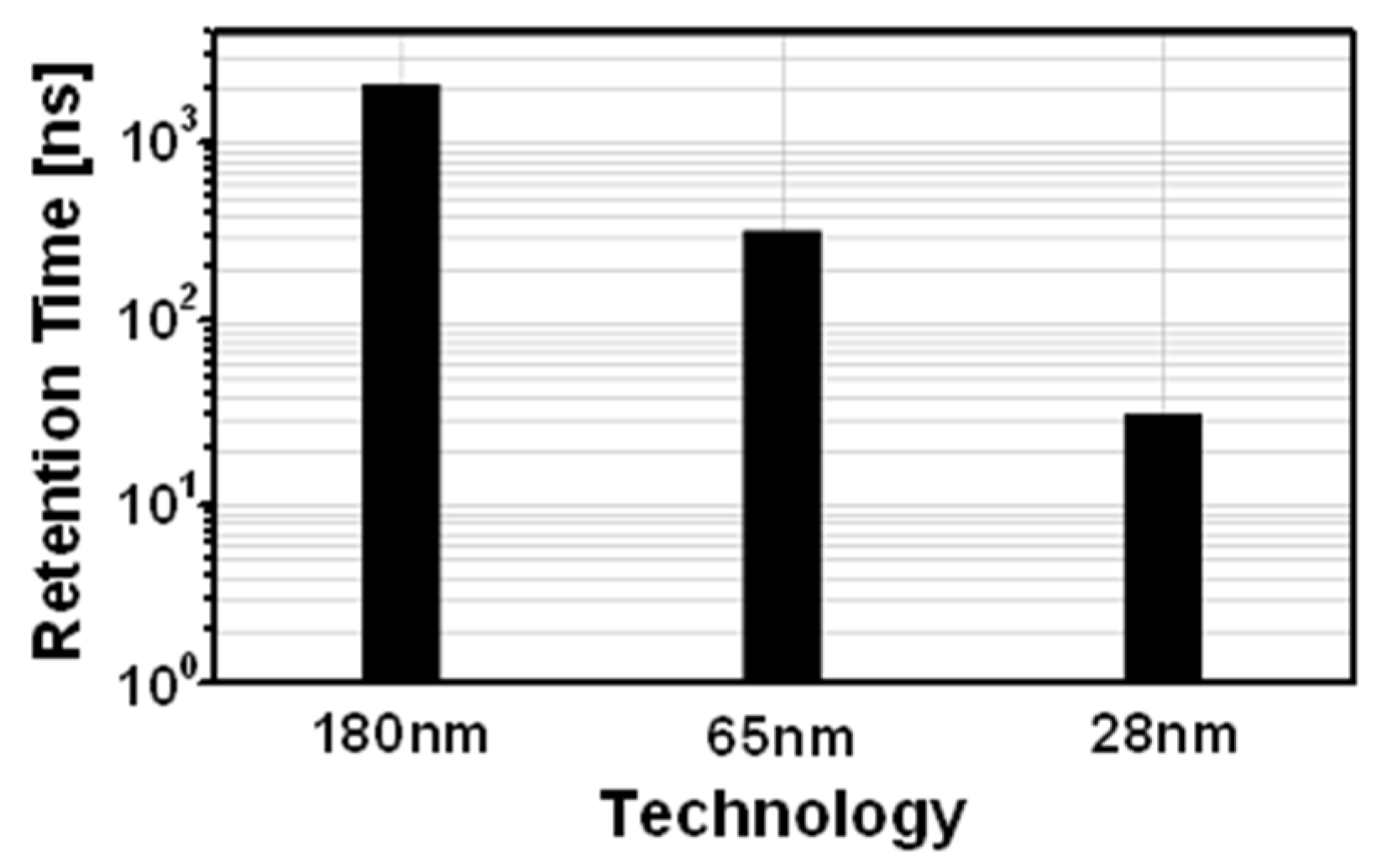
| Retention time | 22.4 ns | 50 ns | 154 µs |
| Storage | MOS gate (<1 fF) | MOS gate (<1 fF) | MOS gate (<1 fF) |
| Supply voltage | 1.1 V | 1.2 V | 0.7 V |
| Process | 28 nm (Converted) | 28 nm (Converted) | 28 nm FD-SOI |
| 2T [20] | 2T [21] | 3T [22] | 3T [29] | 3T [30] | 4T [23] | This Work | ||
|---|---|---|---|---|---|---|---|---|
| Bitcell Schematic |  |  |  |  |  |  |  | |
| Process | 65 nm | 65 nm LP | 65 nm LP | 65 nm LP | 180 nm | 28 nm FD-SOI | 28 nm | |
| Bitcell Size | 0.275 μm2 | 0.478 μm2 | 0.627 μm2 | 0.674 μm2 | 6.97 μm2 | 0.23 μm2 | 0.286 μm2 | |
| Retention Time | 10 μs @ 85°C | 276.5 μs @ 85°C | 1.25 ms @ 85°C | 325 μs @ 85°C | 0.8 ms @ 27°C | 154 μs @ 85°C | Static | |
| Maximum Freq. | 2 GHz | 667 MHz | NA | 1 GHz | 40 MHz | 66 MHz | 100 MHz | 667 MHz |
| VDD Range | 0.7–1.1 V | 0.8–1.4 V | 0.8–1.3 V | 0.8–1.2 V | 0.6–1.2 V | 0.6–0.9 V | 0.7–1.2 V | 0.9–1.2 V |
| Temp. Range | 25–85 °C | 25–85 °C | 25–85 °C | 25–85 °C | 27 °C | 0–85 °C | −25–85 °C | |
| Write Access Time | NA | 0.21 ns @ 85 °C | 0.27 ns @ 85 °C | 1.5 ns @ 85 °C | 1.3 ns @ 27 °C | 0.46–0.67 ns @ 27 °C | <0.3 ns @ 85 °C, TT | |
| Read Access Time | NA | 0.46 ns @ 85 °C | 0.61 ns @ 85 °C | 1 ns @ 85 °C | NA | <3 ns @ 27 °C | <0.3 ns @ 85 °C, TT | |
| Additional Bit/Word Line? | No | No | No | Yes | Yes | No | No | |
| Need Boosted Voltage? | Yes | Yes | Yes | Yes | No | Yes | No | |
| Need Refresh? | Yes | Yes | Yes | Yes | Yes | Yes | No | |
| Retention Power | 508 mW/2 Mb @ 85 °C | 1.16 mW/Mb @ 85 °C | 1.25 mW/Mb @ 85 °C | NA | 1 μW/2 kb @ 27 °C | 909 nW/8 kb @ 85 °C | 22.5 μW/4 kb @ 85 °C, TT | |
| 6T SRAM [34] | 8T SRAM [35] | 2T eDRAM [21] | 3T eDRAM [22] | This Work | |||
|---|---|---|---|---|---|---|---|
| BitcellSchematic | 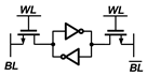 |  |  |  | 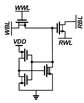 | ||
| Process | 28 nm | 28 nm | 28 nm | 28 nm | 28 nm | ||
| Normalized Area | 1 X | 1.36 X | 0.39 X | 0.58 X | 0.79 X | ||
| Bitcell Size | 0.36 μm2 | 0.491 μm2 | 0.14 μm2 | 0.209 μm2 | 0.286 μm2 | ||
| Retention Time | Static | Static | 17.2 ns | 42.1 ns | Static | ||
| Bitcell Access | Shared R/W | Decoupled R/W | Decoupled R/W | Decoupled R/W | Decoupled R/W | ||
| Storage | Latch | Latch | MOS gate (<1 fF) | MOS gate (<1 fF) | MOS gate (<1 fF) | ||
| Supply Voltage | 0.9 V | 0.9 V | 0.9 V | 0.9 V | 0.9 V | ||
| Static Power/bit | 50 nW | 69 nW | 0.16 nW | 1.51 nW | FS (−25 °C) | TT (25 °C) | SF (85 °C) |
| 0.07 nW | 2.2 nW | 47.4 nW | |||||
Publisher’s Note: MDPI stays neutral with regard to jurisdictional claims in published maps and institutional affiliations. |
© 2022 by the authors. Licensee MDPI, Basel, Switzerland. This article is an open access article distributed under the terms and conditions of the Creative Commons Attribution (CC BY) license (https://creativecommons.org/licenses/by/4.0/).
Share and Cite
Kim, S.; Park, J.-E. Pseudo-Static Gain Cell of Embedded DRAM for Processing-in-Memory in Intelligent IoT Sensor Nodes. Sensors 2022, 22, 4284. https://doi.org/10.3390/s22114284
Kim S, Park J-E. Pseudo-Static Gain Cell of Embedded DRAM for Processing-in-Memory in Intelligent IoT Sensor Nodes. Sensors. 2022; 22(11):4284. https://doi.org/10.3390/s22114284
Chicago/Turabian StyleKim, Subin, and Jun-Eun Park. 2022. "Pseudo-Static Gain Cell of Embedded DRAM for Processing-in-Memory in Intelligent IoT Sensor Nodes" Sensors 22, no. 11: 4284. https://doi.org/10.3390/s22114284
APA StyleKim, S., & Park, J.-E. (2022). Pseudo-Static Gain Cell of Embedded DRAM for Processing-in-Memory in Intelligent IoT Sensor Nodes. Sensors, 22(11), 4284. https://doi.org/10.3390/s22114284