
Advances in Plasmonic Sensing at the NIR—A Review

 ,
,  , and
, and 
Abstract
:1. Introduction
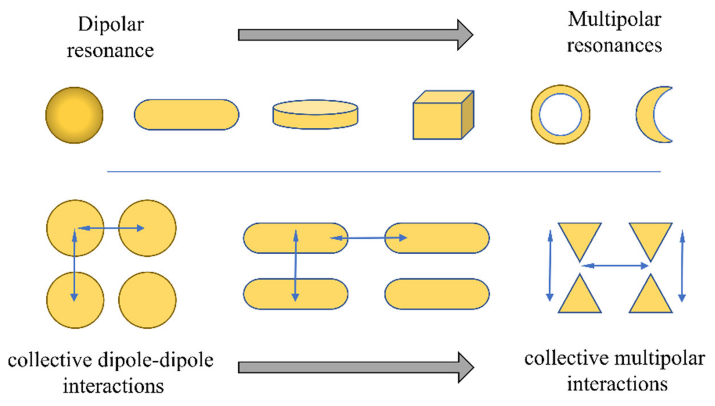
1.1. Localized Surface Plasmon Resonances
1.2. Nanoparticle Fabrication
1.3. Optical Fiber Functionalization and Sensing Applications
1.4. LSPR Sensing Parameters
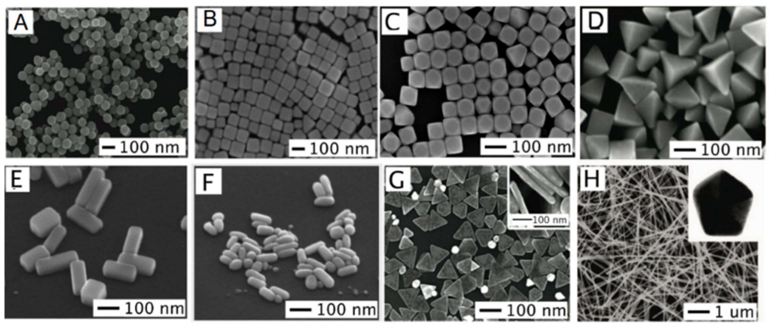
2. Nanostructures
2.1. Introduction
2.2. Spheres
2.3. Triangles
2.4. Stars
2.5. Cubes
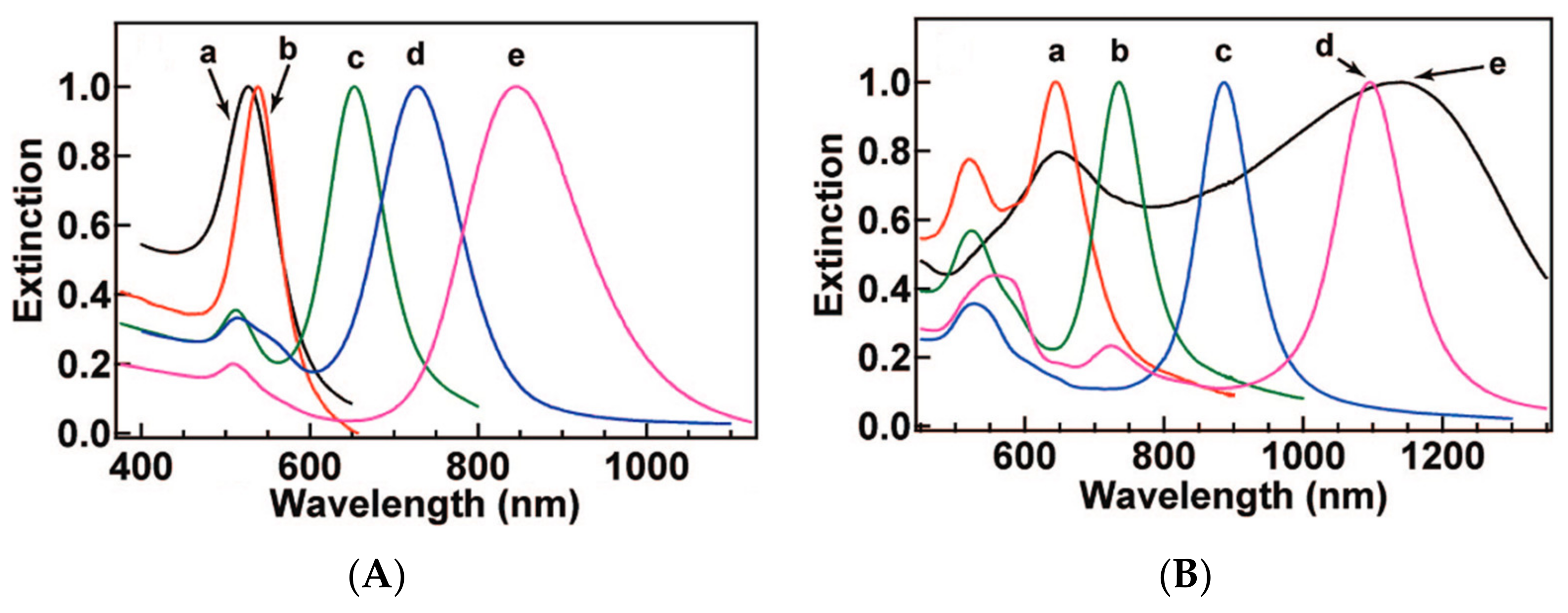
2.6. Nanorods
2.7. Rings and Trimmers
2.8. Pillars
2.9. Shells
2.10. Crescents
2.11. Arrays
2.12. Superstructures
3. Materials
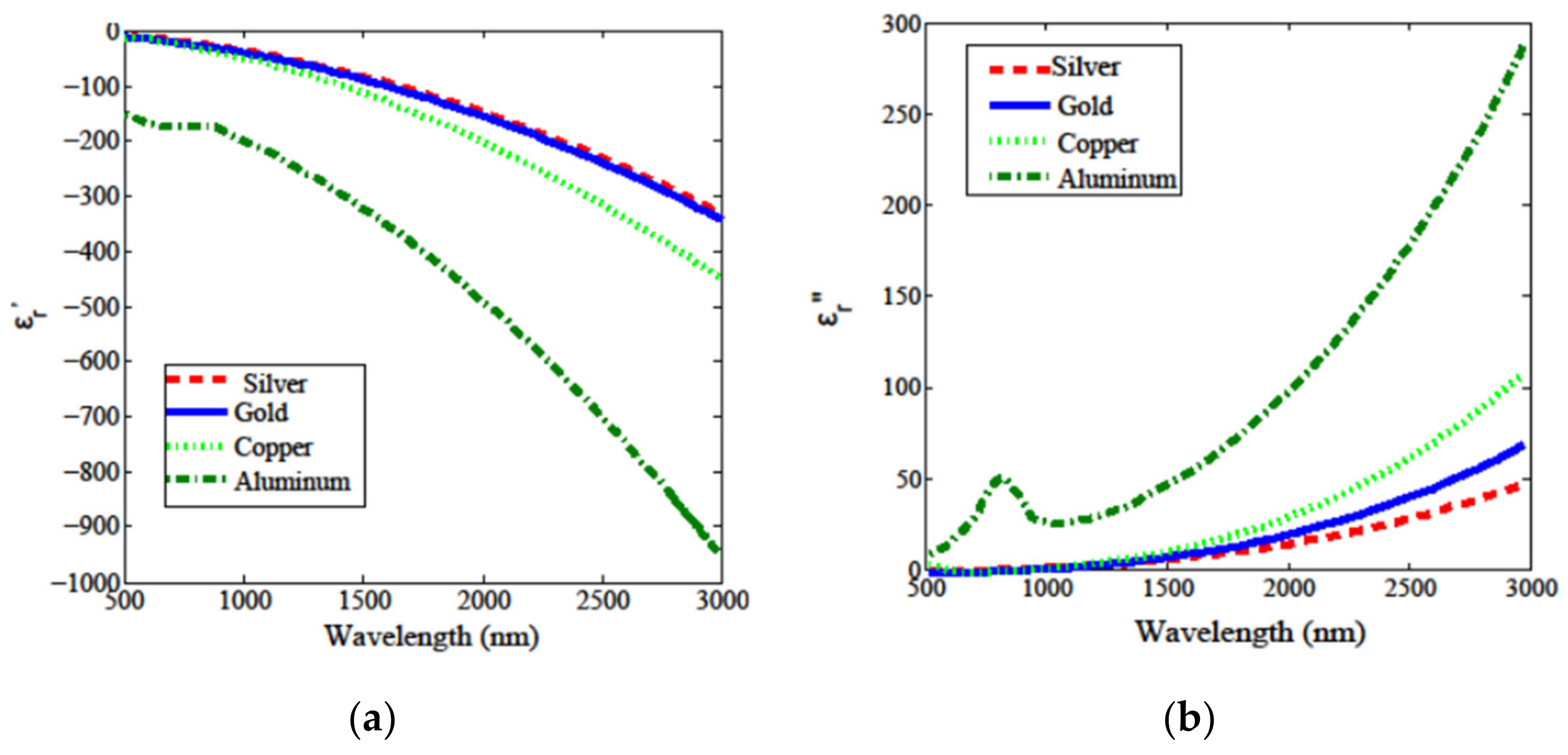
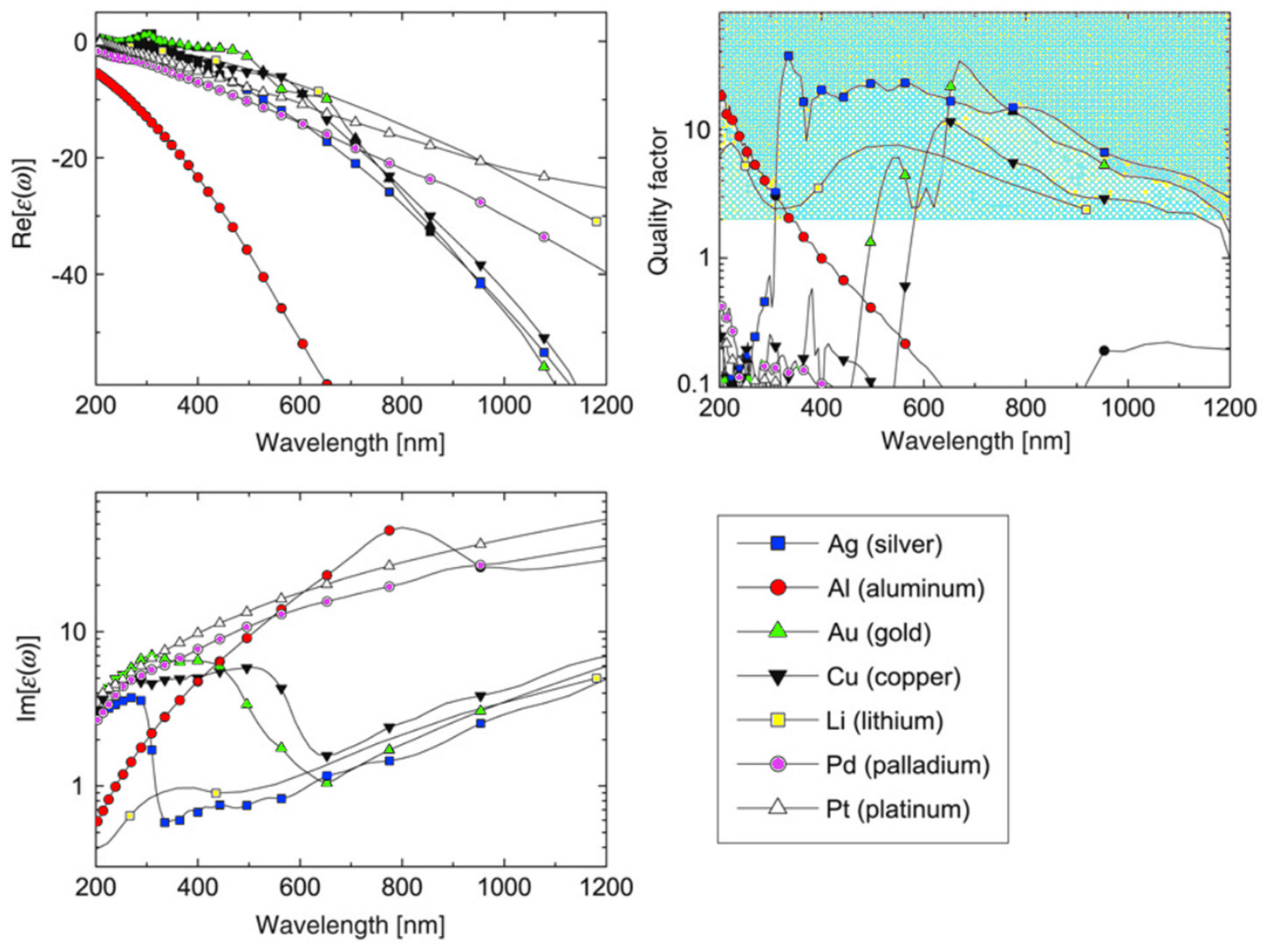
3.1. Metals
3.2. Transparent Conductive Oxides
3.3. Transition-Metal Oxides
4. Discussion
Author Contributions
Funding
Institutional Review Board Statement
Informed Consent Statement
Data Availability Statement
Acknowledgments
Conflicts of Interest
References
- Borisov, S.M.; Wolfbeis, O.S. Optical Biosensors. Chem. Rev. 2008, 108, 423–461. [Google Scholar] [CrossRef]
- Arasu, P.T.; Al-Qazwini, Y.; Onn, B.I.; Noor, A.S.M. Fiber Bragg grating based surface plasmon resonance sensor utilizing FDTD for alcohol detection applications. In Proceedings of the ICP 2012—3rd International Conference on Photonics 2012, Penang, Malaysia, 1–3 October 2012; pp. 93–97. [Google Scholar] [CrossRef]
- Burgmeier, J.; Feizpour, A.; Schade, W.; Reinhard, B.M. Plasmonic nanoshell functionalized etched fiber Bragg gratings for highly sensitive refractive index measurements. Opt. Lett. 2015, 40, 546–549. [Google Scholar] [CrossRef] [PubMed]
- Halas, N.J.; Lal, S.; Chang, W.-S.; Link, S.; Nordlander, P. Plasmons in Strongly Coupled Metallic Nanostructures. Chem. Rev. 2011, 111, 3913–3961. [Google Scholar] [CrossRef] [PubMed]
- Anker, J.N.; Hall, W.P.; Lyandres, O.; Shah, N.C.; Zhao, J.; Van Duyne, R.P. Biosensing with plasmonic nanosensors. Nat. Mater. 2008, 7, 442–453. [Google Scholar] [CrossRef]
- Gao, M.; Zheng, X.; Khan, I.; Cai, H.; Lan, J.; Liu, J.; Wang, J.; Wu, J.; Huang, S.; Li, S.; et al. Resonant light absorption and plasmon tunability of lateral triangular Au nanoprisms array. Phys. Lett. A 2019, 383, 125881. [Google Scholar] [CrossRef]
- Bochenkov, V.E.; Shabatina, T.I. Chiral Plasmonic Biosensors. Biosensors 2018, 8, 120. [Google Scholar] [CrossRef] [PubMed] [Green Version]
- Le Ru, E.; Etchegoin, P. Principles of Surface-Enhanced Raman Spectroscopy; ScienceDirect: Amsterdam, The Netherlands, 2008. [Google Scholar]
- Yu, H.; Peng, Y.; Yang, Y.; Li, Z.-Y. Plasmon-enhanced light–matter interactions and applications. Npj Comput. Mater. 2019, 5, 45. [Google Scholar] [CrossRef]
- Enoch, S.; Bonod, N. Plasmonics—From Basics to Advanced Topics; Springer: Berlin/Heidelberg, Germany, 2012; Volume 167. [Google Scholar]
- Bohm, D.; Pines, D. A Collective Description of Electron Interactions. I. Magnetic Interactions. Phys. Rev. 1951, 82, 625. [Google Scholar] [CrossRef]
- Sepúlveda, B.; Angelomé, P.C.; Lechuga, L.M.; Liz-Marzán, L.M. LSPR-based nanobiosensors. Nano Today 2009, 4, 244–251. [Google Scholar] [CrossRef]
- Zia, R.; Schuller, J.A.; Chandran, A.; Brongersma, M.L. Plasmonics: The next chip-scale technology. Mater. Today 2006, 9, 20–27. [Google Scholar] [CrossRef]
- Atwater, H.A.; Polman, A. Plasmonics for improved photovoltaic devices. Nat. Mater. 2010, 9, 205–213. [Google Scholar] [CrossRef] [PubMed]
- Li, J.; Xue, X.; Fan, Y.; Ma, L.; Zou, S.; Xie, Z.; Zhang, Z. Standing wave type localized surface plasmon resonance of multifold Ag nanorods. Nanotechnology 2018, 30, 55703. [Google Scholar] [CrossRef] [PubMed]
- Petryayeva, E.; Krull, U.J. Localized surface plasmon resonance: Nanostructures, bioassays and biosensing—A review. Anal. Chim. Acta 2011, 706, 8–24. [Google Scholar] [CrossRef] [PubMed]
- Willets, K.A.; Van Duyne, R.P. Localized Surface Plasmon Resonance Spectroscopy and Sensing. Annu. Rev. Phys. Chem. 2007, 58, 267–297. [Google Scholar] [CrossRef] [PubMed] [Green Version]
- Li, Z.; Wang, W.; Yin, Y. Colloidal Assembly and Active Tuning of Coupled Plasmonic Nanospheres. Trends Chem. 2020, 2, 593–608. [Google Scholar] [CrossRef]
- Cao, J.; Sun, T.; Grattan, K.T. Gold nanorod-based localized surface plasmon resonance biosensors: A review. Sens. Actuators B Chem. 2014, 195, 332–351. [Google Scholar] [CrossRef]
- West, P.; Ishii, S.; Naik, G.; Emani, N.; Shalaev, V.; Boltasseva, A. Searching for better plasmonic materials. Laser Photonics Rev. 2010, 4, 795–808. [Google Scholar] [CrossRef] [Green Version]
- Ghosh, G. Handbook of Optical Constants of Solids, 1st ed.; ScienceDirect: Amsterdam, The Netherlands, 1996; Volume III. [Google Scholar]
- Zhang, K.-L.; Hou, Z.-L.; Kong, L.-B.; Fang, H.-M.; Zhan, K.-T. Origin of Negative Imaginary Part of Effective Permittivity of Passive Materials. Chin. Phys. Lett. 2017, 34, 97701. [Google Scholar] [CrossRef]
- Larsson, E.M.; Alegret, J.; Käll, M.; Sutherland, D.S. Sensing Characteristics of NIR Localized Surface Plasmon Resonances in Gold Nanorings for Application as Ultrasensitive Biosensors. Nano Lett. 2007, 7, 1256–1263. [Google Scholar] [CrossRef] [PubMed]
- Neil, N.D.M.; Ashcroft, W. Solid State Physics; Holt, Rinehart and Winston: New York, NY, USA, 1976. [Google Scholar]
- Chen, K.-P.; Drachev, V.P.; Borneman, J.D.; Kildishev, A.V.; Shalaev, V.M. Drude Relaxation Rate in Grained Gold Nanoantennas. Nano Lett. 2010, 10, 916–922. [Google Scholar] [CrossRef]
- Derkachova, A.; Kolwas, K.; Demchenko, I. Dielectric Function for Gold in Plasmonics Applications: Size Dependence of Plasmon Resonance Frequencies and Damping Rates for Nanospheres. Plasmonics 2016, 11, 941–951. [Google Scholar] [CrossRef] [Green Version]
- Jiang, Y.; Pillai, S.; Green, M.A. Grain boundary effects on the optical constants and Drude relaxation times of silver films. J. Appl. Phys. 2016, 120, 233109. [Google Scholar] [CrossRef]
- Suresh, S. Semiconductor Nanomaterials, Methods and Applications: A Review. Nanosci. Nanotechnol. 2013, 3, 62–74. [Google Scholar] [CrossRef]
- Bangal, M.; Ashtaputre, S.; Marathe, S.; Ethiraj, A.; Hebalkar, N.; Gosavi, S.W.; Urban, J.; Kulkarni, S.K. Semiconductor Nanoparticles. Hyperfine Interact. 2005, 160, 81–94. [Google Scholar] [CrossRef]
- Zhang, Y.; Cheng, J.; Liu, W. Characterization and Relaxation Properties of a Series of Monodispersed Magnetic Nanoparticles. Sensors 2019, 19, 3396. [Google Scholar] [CrossRef] [PubMed] [Green Version]
- Trügler, A.; Tinguely, J.-C.; Krenn, J.R.; Hohenau, A.; Hohenester, U. Influence of surface roughness on the optical properties of plasmonic nanoparticles. Phys. Rev. B 2011, 83, 15–18. [Google Scholar] [CrossRef] [Green Version]
- Niu, Y.; Yu, M.; Meka, A.K.; Liu, Y.; Zhang, J.; Yang, Y.; Yu, C. Understanding the contribution of surface roughness and hydrophobic modification of silica nanoparticles to enhanced therapeutic protein delivery. J. Mater. Chem. B 2016, 4, 212–219. [Google Scholar] [CrossRef] [PubMed]
- Naik, G.V.; Shalaev, V.M.; Boltasseva, A. Alternative Plasmonic Materials: Beyond Gold and Silver. Adv. Mater. 2013, 25, 3264–3294. [Google Scholar] [CrossRef]
- Mehlhorn, A.; Rahimi, P.; Joseph, Y. Aptamer-Based Biosensors for Antibiotic Detection: A Review. Biosensors 2018, 8, 54. [Google Scholar] [CrossRef] [PubMed] [Green Version]
- Nezami, A.; Nosrati, R.; Golichenari, B.; Rezaee, R.; Chatzidakis, G.I.; Tsatsakis, A.M.; Karimi, G. Nanomaterial-based aptasensors and bioaffinity sensors for quantitative detection of 17β-estradiol. TrAC Trends Anal. Chem. 2017, 94, 95–105. [Google Scholar] [CrossRef]
- Allsop, T.; Neal, R. A Review: Evolution and Diversity of Optical Fibre Plasmonic Sensors. Sensors 2019, 19, 4874. [Google Scholar] [CrossRef] [PubMed] [Green Version]
- Smitha, S.; Gopchandran, K.; Smijesh, N.; Philip, R. Size-dependent optical properties of Au nanorods. Prog. Nat. Sci. 2013, 23, 36–43. [Google Scholar] [CrossRef] [Green Version]
- Polley, N.; Basak, S.; Hass, R.; Pacholski, C. Fiber optic plasmonic sensors: Providing sensitive biosensor platforms with minimal lab equipment. Biosens. Bioelectron. 2019, 132, 368–374. [Google Scholar] [CrossRef] [PubMed]
- Shukla, S.; Kushwaha, C.S.; Guner, T.; Demir, M.M. Chemically modified optical fibers in advanced technology: An overview. Opt. Laser Technol. 2019, 115, 404–432. [Google Scholar] [CrossRef]
- Belekoukia, M.; Tan, J.Z.; Andresen, J.M.; Wang, H.; Maroto-Valer, M.M.; Xuan, J. Laser Induced Plasmonic Heating with Au Decorated TiO2 Nanoparticles. Energy Procedia 2019, 158, 5647–5652. [Google Scholar] [CrossRef]
- Barnes, W.; Dereux, A.; Ebbesen, T. Surface plasmon subwavelength optics. Nature 2003, 424, 824–830. [Google Scholar] [CrossRef]
- Ozbay, E. Plasmonics: Merging Photonics and Electronics at Nanoscale Dimensions. Science 2006, 311, 189–193. [Google Scholar] [CrossRef]
- Pyayt, A.L.; Wiley, B.; Xia, Y.; Chen, A.; Dalton, L. Integration of photonic and silver nanowire plasmonic waveguides. Nat. Nanotechnol. 2008, 3, 660–665. [Google Scholar] [CrossRef]
- Wang, Z.; Zhang, Z.M.; Quan, X.; Cheng, P. A numerical study on effects of surrounding medium, material, and geometry of nanoparticles on solar absorption efficiencies. Int. J. Heat Mass Transf. 2018, 116, 825–832. [Google Scholar] [CrossRef]
- Kabashin, A.V.; Evans, P.; Pastkovsky, S.; Hendren, W.; Wurtz, G.; Atkinson, R.; Pollard, R.; Podolskiy, V.A.; Zayats, A. Plasmonic nanorod metamaterials for biosensing. Nat. Mater. 2009, 8, 867–871. [Google Scholar] [CrossRef]
- Prabowo, B.A.; Purwidyantri, A.; Liu, K.-C. Surface Plasmon Resonance Optical Sensor: A Review on Light Source Technology. Biosensors 2018, 8, 80. [Google Scholar] [CrossRef] [Green Version]
- Aliofkhazraei, M. Handbook of Nanoparticles; Springer International Publishing: Cham, Switzerland, 2015. [Google Scholar]
- Yao, Q.; Yuan, X.; Fung, V.; Yu, Y.; Leong, D.T.; Jiang, D.-E.; Xie, J. Understanding seed-mediated growth of gold nanoclusters at molecular level. Nat. Commun. 2017, 8, 1–11. [Google Scholar] [CrossRef] [Green Version]
- Niu, W.; Zhang, L.; Guobao, X. Seed-Mediated Growth of Noble Metal Nanocrystals: Crystal Growth and Shape Control Wenxin. Nanoscale 2013, 207890. [Google Scholar] [CrossRef]
- Ye, X.; Jin, L.; Caglayan, H.; Chen, J.; Xing, G.; Zheng, C.; Doan-Nguyen, V.; Kang, Y.; Engheta, N.; Kagan, C.R.; et al. Improved Size-Tunable Synthesis of Monodisperse Gold Nanorods through the Use of Aromatic Additives. ACS Nano 2012, 6, 2804–2817. [Google Scholar] [CrossRef] [PubMed]
- Xia, H.; XiaHou, Y.; Zhang, P.; Ding, W.; Wang, D. Revitalizing the Frens Method to Synthesize Uniform, Quasi-Spherical Gold Nanoparticles with Deliberately Regulated Sizes from 2 to 330 nm. Langmuir 2016, 32, 5870–5880. [Google Scholar] [CrossRef] [PubMed]
- Alkilany, A.M.; Yaseen, A.I.B.; Kailani, M.H. Synthesis of Monodispersed Gold Nanoparticles with Exceptional Colloidal Stability with Grafted Polyethylene Glycol- g -polyvinyl Alcohol. J. Nanomater. 2015, 2015, 1–9. [Google Scholar] [CrossRef]
- Sperling, R.A.; Parak, W.J. Surface modification, functionalization and bioconjugation of colloidal inorganic nanoparticles. Philos. Trans. R. Soc. A Math. Phys. Eng. Sci. 2010, 368, 1333–1383. [Google Scholar] [CrossRef]
- Li, P.; Wu, Y.; Li, D.; Su, X.; Luo, C.; Wang, Y.; Hu, J.; Li, G.; Jiang, H.; Zhang, W. Seed-Mediated Synthesis of Tunable-Aspect-Ratio Gold Nanorods for Near-Infrared Photoacoustic Imaging. Nanoscale Res. Lett. 2018, 13, 313. [Google Scholar] [CrossRef] [PubMed] [Green Version]
- Wu, D.; Xu, X.; Liu, X. Tunable near-infrared optical properties of three-layered metal nanoshells. J. Chem. Phys. 2008, 129, 74711. [Google Scholar] [CrossRef] [PubMed]
- Jauffred, L.; Samadi, A.; Klingberg, H.; Bendix, P.M.; Oddershede, L.B. Plasmonic Heating of Nanostructures. Chem. Rev. 2019, 119, 8087–8130. [Google Scholar] [CrossRef]
- Rodríguez-Cantó, P.; Martínez-Marco, M.; Rodríguez-Fortuño, F.J.; Tomás-Navarro, B.; Ortuño, R.; Peransí-Llopis, S.; Martínez, A. Demonstration of near infrared gas sensing using gold nanodisks on functionalized silicon. Opt. Express 2011, 19, 7664–7672. [Google Scholar] [CrossRef] [Green Version]
- Altansukh, B.; Yao, J.; Wang, D. Synthesis and characterization of gold nanorods by a seeding growth method. J. Nanosci. Nanotechnol. 2009, 9, 1300–1303. [Google Scholar] [CrossRef] [PubMed]
- Jana, N.R.; Gearheart, L.; Murphy, C.J. Wet Chemical Synthesis of High Aspect Ratio Cylindrical Gold Nanorods. J. Phys. Chem. B 2001, 105, 4065–4067. [Google Scholar] [CrossRef]
- Koeppl, S.; Solenthaler, C.; Caseri, W.; Spolenak, R. Towards a Reproducible Synthesis of High Aspect Ratio Gold Nanorods. J. Nanomater. 2010, 2011, 1–13. [Google Scholar] [CrossRef]
- Link, S.; El-Sayed, M.A. Erratum: Simulation of the optical absorption spectra of gold nanorods as a function of their aspect ratio and the effect of the medium dielectric constant (Journal of Physical Chemistry B (1999) 103B). J. Phys. Chem. B 2005, 109, 10531–10532. [Google Scholar] [CrossRef] [Green Version]
- Brioude, A.; Jiang, X.C.; Pileni, M.P. Optical Properties of Gold Nanorods: DDA Simulations Supported by Experiments. J. Phys. Chem. B 2005, 109, 13138–13142. [Google Scholar] [CrossRef]
- Wang, Y.-N.; Wei, W.-T.; Yang, C.-W.; Huang, M.H. Seed-Mediated Growth of Ultralong Gold Nanorods and Nanowires with a Wide Range of Length Tunability. Langmuir 2013, 29, 10491–10497. [Google Scholar] [CrossRef] [PubMed]
- Wu, C.; Zhou, X.; Wei, J. Localized Surface Plasmon Resonance of Silver Nanotriangles Synthesized by a Versatile Solution Reaction. Nanoscale Res. Lett. 2015, 10, 1–6. [Google Scholar] [CrossRef] [PubMed] [Green Version]
- Sekhon, J.S.; Verma, S. Controlling the LSPR properties of Au triangular nanoprisms and nanoboxes by geometrical parameter: A numerical investigation. J. Mod. Opt. 2014, 62, 435–440. [Google Scholar] [CrossRef] [Green Version]
- Zhang, B.; Sato, R.; Tanaka, M.; Takeda, Y. Spectral dependence of third-order susceptibility of Au triangular nanoplates. Sci. Rep. 2020, 10, 1–6. [Google Scholar] [CrossRef]
- Haes, A.J.; Van Duyne, R.P. A nanoscale optical biosensor: Sensitivity and selectivity of an approach based on the localized surface plasmon resonance spectroscopy of triangular silver nanoparticles. J. Am. Chem. Soc. 2002, 124, 10596–10604. [Google Scholar] [CrossRef]
- Corbierre, M.K.; Beerens, J.; Lennox, R.B. Gold Nanoparticles Generated by Electron Beam Lithography of Gold(I)−Thiolate Thin Films. Chem. Mater. 2005, 17, 5774–5779. [Google Scholar] [CrossRef]
- Trasobares, J.; Vaurette, F.; François, M.; Romijn, H.; Codron, J.-L.; Vuillaume, D.; Theron, D.; Clément, N. High speed e-beam lithography for gold nanoarray fabrication and use in nanotechnology. Beilstein J. Nanotechnol. 2014, 5, 1918–1925. [Google Scholar] [CrossRef] [PubMed] [Green Version]
- Wu, W.; Kim, E.; Williams, R.S. Optical Metamaterials at Near and Mid IR Range Fabricated by Nanoimprint Lithography. Appl. Phys. A Mater. Sci. Process. 2007, 87, 143–150. [Google Scholar] [CrossRef] [Green Version]
- Chang, C.-Y.; Lin, H.-T.; Lai, M.-S.; Shieh, T.-Y.; Peng, C.-C.; Shih, M.-H.; Tung, Y.-C. Flexible Localized Surface Plasmon Resonance Sensor with Metal–Insulator–Metal Nanodisks on PDMS Substrate. Sci. Rep. 2018, 8, 1–8. [Google Scholar] [CrossRef] [PubMed]
- Cattoni, A.; Ghenuche, P.; Haghiri-Gosnet, A.-M.; Decanini, D.; Chen, J.; Pelouard, J.-L.; Collin, S. λ3/1000 Plasmonic Nanocavities for Biosensing Fabricated by Soft UV Nanoimprint Lithography. Nano Lett. 2011, 11, 3557–3563. [Google Scholar] [CrossRef]
- Xie, S.-Q.; Wan, J.; Lu, B.-R.; Sun, Y.; Chen, Y.; Qu, X.-P.; Liu, R. A nanoimprint lithography for fabricating SU-8 gratings for near-infrared to deep-UV application. Microelectron. Eng. 2008, 85, 914–917. [Google Scholar] [CrossRef]
- Aizpurua, J.; Hanarp, P.; Sutherland, D.S.; Käll, M.; Bryant, G.W.; De Abajo, F.J.G. Optical Properties of Gold Nanorings. Phys. Rev. Lett. 2003, 90, 57401. [Google Scholar] [CrossRef] [PubMed] [Green Version]
- Toma, M.; Cho, K.; Wood, J.B.; Corn, R.M. Gold Nanoring Arrays for Near Infrared Plasmonic Biosensing. Plasmonics 2013, 9, 765–772. [Google Scholar] [CrossRef]
- Rodríguez-Fortuño, F.J.; Martínez-Marco, M.; Tomás-Navarro, B.; Ortuño, R.; Martí, J.; Martínez, A.; Rodríguez-Cantó, P.J. Highly-sensitive chemical detection in the infrared regime using plasmonic gold nanocrosses. Appl. Phys. Lett. 2011, 98, 133118. [Google Scholar] [CrossRef]
- Da Silva, A.G.M.; Rodrigues, T.S.; Haigh, S.J.; Camargo, P.H.C. Galvanic replacement reaction: Recent developments for engineering metal nanostructures towards catalytic applications. Chem. Commun. 2017, 53, 7135–7148. [Google Scholar] [CrossRef] [PubMed]
- Wang, C.; Wang, L.; Long, R.; Ma, L.; Wang, L.; Li, Z.; Xiong, Y. Anisotropic growth of palladium twinned nanostructures controlled by kinetics and their unusual activities in galvanic replacement. J. Mater. Chem. 2012, 22, 8195–8198. [Google Scholar] [CrossRef]
- Bhol, P.; Bhavya, M.B.; Swain, S.; Saxena, M.; Samal, A.K. Modern Chemical Routes for the Controlled Synthesis of Anisotropic Bimetallic Nanostructures and Their Application in Catalysis. Front. Chem. 2020, 8. [Google Scholar] [CrossRef]
- Smythe, E.J.; Dickey, M.D.; Whitesides, G.M.; Capasso, F. A Technique to Transfer Metallic Nanoscale Patterns to Small and Non-Planar Surfaces. ACS Nano 2008, 3, 59–65. [Google Scholar] [CrossRef] [PubMed] [Green Version]
- Lin, Y.; Zou, Y.; Mo, Y.; Guo, J.; Lindquist, R.G. E-Beam Patterned Gold Nanodot Arrays on Optical Fiber Tips for Localized Surface Plasmon Resonance Biochemical Sensing. Sensors 2010, 10, 9397–9406. [Google Scholar] [CrossRef]
- Zeng, X.; Jradi, S.; Proust, J.; Bachelot, R.; Zhang, Z.P.; Royer, P.; Plain, J. Direct functionalization of an optical fiber by a plasmonic nanosensor. Opt. Lett. 2011, 36, 2919–2921. [Google Scholar] [CrossRef] [PubMed]
- Manoharan, H.; Kc, D.; Sai, V.V.R. Controlled In Situ Seed-Mediated Growth of Gold and Silver Nanoparticles on an Optical Fiber Platform for Plasmonic Sensing Applications. Plasmonics 2019, 15, 51–60. [Google Scholar] [CrossRef]
- Nafisah, S.; Morsin, M.; Jumadi, N.A.; Nayan, N.; Shah, N.S.M.; Razali, N.L.; Anrnisa, N.Z. Improved Sensitivity and Selectivity of Direct Localized Surface Plasmon Resonance Sensor Using Gold Nanobipyramids for Glyphosate Detection. IEEE Sens. J. 2019, 20, 1. [Google Scholar] [CrossRef]
- Heidemann, B.R.; Chiamenti, I.; Oliveira, M.M.; Muller, M.; Fabris, J.L. Functionalized Long Period Grating—Plasmonic Fiber Sensor Applied to the Detection of Glyphosate in Water. J. Light. Technol. 2017, 36, 863–870. [Google Scholar] [CrossRef]
- Dos Santos, P.; Jorge, P.; De Almeida, J.M.; Coelho, L. Low-Cost Interrogation System for Long-Period Fiber Gratings Applied to Remote Sensing. Sensors 2019, 19, 1500. [Google Scholar] [CrossRef] [Green Version]
- Li, D.; Zhang, Y.; Guo, Q.; Sun, X.; Zhang, H.; Wang, S.; Birech, Z.; Hu, J. An efficient LSPR method to quantitatively detect dimethoate: Development, characterization and evaluation. PLoS ONE 2020, 15, e0239632. [Google Scholar] [CrossRef]
- Sadani, K.; Nag, P.; Mukherji, S. LSPR based optical fiber sensor with chitosan capped gold nanoparticles on BSA for trace detection of Hg (II) in water, soil and food samples. Biosens. Bioelectron. 2019, 134, 90–96. [Google Scholar] [CrossRef] [PubMed]
- Zhong, X.; Ma, L.; Yin, G.; Gan, M.; Wei, Y. Hg2+ Optical Fiber Sensor Based on LSPR with PDDA-Templated AuNPs and CS/PAA Bilayers. Appl. Sci. 2020, 10, 4845. [Google Scholar] [CrossRef]
- Sherry, L.J.; Chang, S.-H.; Schatz, A.G.C.; Van Duyne, R.P.; Wiley, B.J.; Xia, Y. Localized Surface Plasmon Resonance Spectroscopy of Single Silver Nanocubes. Nano Lett. 2005, 5, 2034–2038. [Google Scholar] [CrossRef]
- Nicoletti, O.; De La Peña, F.; Leary, R.K.; Holland, D.J.; Ducati, C.; Midgley, P.A. Three-dimensional imaging of localized surface plasmon resonances of metal nanoparticles. Nat. Cell Biol. 2013, 502, 80–84. [Google Scholar] [CrossRef] [PubMed]
- Ringe, E.; McMahon, J.M.; Sohn, K.; Cobley, C.; Xia, Y.; Huang, J.; Schatz, G.C.; Marks, L.D.; Van Duyne, R.P. Unraveling the Effects of Size, Composition, and Substrate on the Localized Surface Plasmon Resonance Frequencies of Gold and Silver Nanocubes: A Systematic Single-Particle Approach. J. Phys. Chem. C 2010, 114, 12511–12516. [Google Scholar] [CrossRef]
- Xu, W.; Liu, H.; Zhou, D.; Chen, X.; Ding, N.; Song, H.; Ågren, H. Localized surface plasmon resonances in self-doped copper chalcogenide binary nanocrystals and their emerging applications. Nano Today 2020, 33, 100892. [Google Scholar] [CrossRef]
- Lu, X.; Zhang, L.; Zhang, T. Nanoslit-microcavity-based narrow band absorber for sensing applications. Opt. Express 2015, 23, 20715–20720. [Google Scholar] [CrossRef]
- Sun, F.; Yang, W.; Du, C.; Chen, Y.; Fu, T.; Shi, D. Optimal Aspect Ratio and Excitation Spectral Region of LSPR Sensors Using Individual Au Dimmeric Nanoplates. Plasmonics 2020, 15, 949–955. [Google Scholar] [CrossRef]
- Slaughter, L.S.; Chang, W.-S.; Swanglap, P.; Tcherniak, A.; Khanal, B.P.; Zubarev, E.R.; Link, S. Single-Particle Spectroscopy of Gold Nanorods beyond the Quasi-Static Limit: Varying the Width at Constant Aspect Ratio. J. Phys. Chem. C 2010, 114, 4934–4938. [Google Scholar] [CrossRef]
- Aizpurua, J.M.; Bryant, G.W.; Richter, L.J.; De Abajo, F.J.G.; Kelley, B.K.; E Mallouk, T. Optical properties of coupled metallic nanorods for field-enhanced spectroscopy. Phys. Rev. B 2005, 71, 235420. [Google Scholar] [CrossRef] [Green Version]
- Encina, E.R.; Coronado, E.A. Resonance Conditions for Multipole Plasmon Excitations in Noble Metal Nanorods. J. Phys. Chem. C 2007, 111, 16796–16801. [Google Scholar] [CrossRef]
- Ghosh, S.K.; Pal, T. Interparticle Coupling Effect on the Surface Plasmon Resonance of Gold Nanoparticles: From Theory to Applications. Chem. Rev. 2007, 107, 4797–4862. [Google Scholar] [CrossRef] [PubMed]
- Lu, M.; Hong, L.; Liang, Y.; Charron, B.; Zhu, H.; Peng, W.; Masson, J.-F. Enhancement of Gold Nanoparticle Coupling with a 2D Plasmonic Crystal at High Incidence Angles. Anal. Chem. 2018, 90, 6683–6692. [Google Scholar] [CrossRef] [PubMed]
- Schweikart, A.; Pazos-Perez, N.; Alvarez-Puebla, R.A.; Fery, A. Controlling inter-nanoparticle coupling by wrinkle-assisted assembly. Soft Matter 2011, 7, 4093–4100. [Google Scholar] [CrossRef]
- Zhang, H.; Cadusch, J.; Kinnear, C.; James, T.; Roberts, A.; Mulvaney, P. Direct Assembly of Large Area Nanoparticle Arrays. ACS Nano 2018, 12, 7529–7537. [Google Scholar] [CrossRef]
- Chung, T.; Lee, S.-Y.; Song, E.Y.; Chun, H.; Lee, B. Plasmonic Nanostructures for Nano-Scale Bio-Sensing. Sensors 2011, 11, 10907–10929. [Google Scholar] [CrossRef]
- Wiley, B.J.; Chen, Y.; McLellan, J.M.; Xiong, Y.J.; Li, Z.Y.; Ginger, D.; Xia, Y.N. Synthesis and optical properties of silver nanobars and nanorice. Nano Lett. 2007, 7, 1032–1036. [Google Scholar] [CrossRef]
- Zhou, H.; Gao, D.; Gao, L. Tunability of Multipolar Plasmon Resonances and Fano Resonances in Bimetallic Nanoshells. Plasmonics 2017, 13, 623–630. [Google Scholar] [CrossRef]
- Becknell, N.; Zheng, C.; Chen, C.; Yu, Y.; Yang, P. Synthesis of PtCo3 polyhedral nanoparticles and evolution to Pt3Co nanoframes. Surf. Sci. 2016, 648, 328–332. [Google Scholar] [CrossRef] [Green Version]
- Girard, M.; Millan, J.A.; de la Cruz, M.O. DNA-Driven Assembly: From Polyhedral Nanoparticles to Proteins Keynote Topic. Annu. Rev. Mater. Sci. 2017, 47, 83–114. [Google Scholar] [CrossRef]
- Polani, S.; Melamed, S.; Burlaka, L.; De La Vega, F.; Zitoun, D. Large-scale synthesis of polyhedral Ag nanoparticles for printed electronics. RSC Adv. 2017, 7, 54326–54331. [Google Scholar] [CrossRef] [Green Version]
- Zhu, Z.; Liu, L.; Liu, Z.; Zhang, Y.; Zhang, Y. Surface-plasmon-resonance-based optical-fibertemperature sensor with high sensitivityand high figure of merit. Opt. Lett. 2017, 42, 2948–2951. [Google Scholar] [CrossRef]
- Lin, Y.; Wang, D.; Hu, J.; Liu, J.; Wang, W.; Guan, J.; Schaller, R.D.; Odom, T.W. Engineering Symmetry-Breaking Nanocrescent Arrays for Nanolasing. Adv. Funct. Mater. 2019, 29, 1–8. [Google Scholar] [CrossRef]
- Talapin, D.V.; Shevchenko, E.V.; Murray, C.B.; Titov, A.V.; Král, P. Dipole−Dipole Interactions in Nanoparticle Superlattices. Nano Lett. 2007, 7, 1213–1219. [Google Scholar] [CrossRef] [PubMed]
- Rycenga, M.; Cobley, C.M.; Zeng, J.; Li, W.; Moran, C.H.; Zhang, Q.; Qin, D.; Xia, Y. Controlling the Synthesis and Assembly of Silver Nanostructures for Plasmonic Applications. Chem. Rev. 2011, 111, 3669–3712. [Google Scholar] [CrossRef] [PubMed] [Green Version]
- Zhu, J.; Li, F.-K. Effect of aspect ratio on the inter-surface plasmonic coupling of tubular gold nanoparticle. Eur. Phys. J. B 2011, 80, 83–87. [Google Scholar] [CrossRef]
- Chen, H.; Kou, X.; Yang, Z.; Ni, W.; Wang, J. Shape- and Size-Dependent Refractive Index Sensitivity of Gold Nanoparticles. Langmuir 2008, 24, 5233–5237. [Google Scholar] [CrossRef] [PubMed]
- Heiligtag, F.J.; Niederberger, M. The fascinating world of nanoparticle research. Mater. Today 2013, 16, 262–271. [Google Scholar] [CrossRef]
- Shafiqa, A.; Aziz, A.A.; Mehrdel, B. Nanoparticle Optical Properties: Size Dependence of a Single Gold Spherical Nanoparticle. J. Phys. Conf. Ser. 2018, 1083, 12040. [Google Scholar] [CrossRef] [Green Version]
- Liz-Marzán, L.M. Tailoring Surface Plasmons through the Morphology and Assembly of Metal Nanoparticles. Langmuir 2006, 22, 32–41. [Google Scholar] [CrossRef] [PubMed]
- Bhatia, P.; Verma, S.; Sinha, M. Tunable plasmonic properties of elongated bimetallic alloys nanoparticles towards deep UV-NIR absorbance and sensing. J. Quant. Spectrosc. Radiat. Transf. 2020, 241, 106751. [Google Scholar] [CrossRef]
- Liusman, C.; Li, S.Z.; Chen, X.D.; Wei, W.; Zhang, H.; Schatz, G.C.; Boey, F.; Mirkin, C.A. Free-standing bimetallic nanorings and nanoring arrays made by on-wire lithography. ACS Nano 2010, 4, 7676–7682. [Google Scholar] [CrossRef]
- Puthukkara AR, P.; Jose, S.T.; Lal, D.S. Chitosan-Stabilized Fe/Ni Bimetallic Nanoparticles for the Removal of Cationic and Anionic Triphenylmethane Dyes from Water. Environ. Nanotechnol. Monit. Manag. 2020, 100295. [Google Scholar] [CrossRef]
- Ma, T.; Liang, F.; Chen, R.; Liu, S.; Zhang, H. Synthesis of Au-Pd Bimetallic Nanoflowers for Catalytic Reduction of 4-Nitrophenol. Nanomaterials 2017, 7, 239. [Google Scholar] [CrossRef] [Green Version]
- Zakaria, R.; Zainuddin, N.A.M.; Raya, S.A.; Alwi, S.A.K.; Anwar, T.; Sarlan, A.; Ahmed, K.; Amiri, I.S. Sensitivity Comparison of Refractive Index Transducer Optical Fiber Based on Surface Plasmon Resonance Using Ag, Cu, and Bimetallic Ag-Cu Layer. Micromachines 2020, 11, 77. [Google Scholar] [CrossRef] [PubMed] [Green Version]
- McGrath, A.J.; Chien, Y.-H.; Cheong, S.; Herman, D.A.J.; Watt, J.; Henning, A.M.; Gloag, L.; Yeh, C.-S.; Tilley, R.D. Gold over Branched Palladium Nanostructures for Photothermal Cancer Therapy. ACS Nano 2015, 9, 12283–12291. [Google Scholar] [CrossRef]
- Hottin, J.; Wijaya, E.; Hay, L.; Maricot, S.; Bouazaoui, M.; Vilcot, J.-P. Comparison of Gold and Silver/Gold Bimetallic Surface for Highly Sensitive Near-infrared SPR Sensor at 1550 nm. Plasmonics 2012, 8, 619–624. [Google Scholar] [CrossRef]
- Chung, T.; Hwang, C.S.H.; Ahn, M.-S.; Jeong, K.-H. Au/Ag Bimetallic Nanocomposites as a Highly Sensitive Plasmonic Material. Plasmonics 2018, 14, 407–413. [Google Scholar] [CrossRef] [Green Version]
- Gao, J.; Ren, X.; Chen, D.; Tang, F.; Ren, J. Bimetallic Ag–Pt hollow nanoparticles: Synthesis and tunable surface plasmon resonance. Scr. Mater. 2007, 57, 687–690. [Google Scholar] [CrossRef]
- Yi, Z.; Xu, X.; Li, X.; Luo, J.; Wu, W.; Tang, Y.; Yi, Y. Facile preparation of Au/Ag bimetallic hollow nanospheres and its application in surface-enhanced Raman scattering. Appl. Surf. Sci. 2011, 258, 212–217. [Google Scholar] [CrossRef]
- Haynes, C.L.; Haes, A.J.; McFarland, A.D.; Van Duyne, R.P. Nanoparticles with Tunable Localized Surface Plasmon Resonances. Top. Fluoresc. Spectrosc. 2005, 8, 47–99. [Google Scholar] [CrossRef]
- Wang, G.-H.; Hilgert, J.; Richter, F.H.; Wang, F.; Bongard, H.-J.; Spliethoff, B.; Weidenthaler, C.; Schüth, F. Platinum–cobalt bimetallic nanoparticles in hollow carbon nanospheres for hydrogenolysis of 5-hydroxymethylfurfural. Nat. Mater. 2014, 13, 293–300. [Google Scholar] [CrossRef]
- Lie, S.Q.; Zou, H.Y.; Chang, Y.; Huang, C.Z. Tuning of the near-infrared localized surface plasmon resonance of Cu2−xSe nanoparticles with lysozyme-induced selective aggregation. RSC Adv. 2014, 4, 55094–55099. [Google Scholar] [CrossRef]
- Centeno, A.; Aid, S.R.; Xie, F. Infra-Red Plasmonic Sensors. Chemosensors 2018, 6, 4. [Google Scholar] [CrossRef] [Green Version]
- Nishikawa, K.; Kishida, Y.; Ito, K.; Tamura, S.-I.; Takeda, Y. Near-infrared localized surface plasmon resonance of self-growing W-doped VO2 nanoparticles at room temperature. Appl. Phys. Lett. 2017, 111, 193102. [Google Scholar] [CrossRef]
- Bastys, V.; Pastoriza-Santos, I.; Rodríguez-González, B.; Vaisnoras, R.; Liz-Marzán, L.M. Formation of Silver Nanoprisms with Surface Plasmons at Communication Wavelengths. Adv. Funct. Mater. 2006, 16, 766–773. [Google Scholar] [CrossRef]
- Kuttner, C.; Mayer, M.; Dulle, M.; Moscoso, A.I.; López-Romero, J.M.; Förster, S.; Fery, A.; Pérez-Juste, J.; Contreras-Cáceres, R. Seeded Growth Synthesis of Gold Nanotriangles: Size Control, SAXS Analysis, and SERS Performance. ACS Appl. Mater. Interfaces 2018, 10, 11152–11163. [Google Scholar] [CrossRef] [PubMed]
- Koetz, J. The Effect of Surface Modification of Gold Nanotriangles for Surface-Enhanced Raman Scattering Performance. Nanomaterials 2020, 10, 2187. [Google Scholar] [CrossRef]
- Rahaman, M.; Moras, S.; He, L.; Madeira, T.I.; Zahn, D.R.T. Fine-tuning of localized surface plasmon resonance of metal nanostructures from near-Infrared to blue prepared by nanosphere lithography. J. Appl. Phys. 2020, 128, 233104. [Google Scholar] [CrossRef]
- Soares, L.; Csáki, A.; Jatschka, J.; Fritzsche, W.; Flores, O.; Franco, R.; Pereira, E. Localized surface plasmon resonance (LSPR) biosensing using gold nanotriangles: Detection of DNA hybridization events at room temperature. Analyst 2014, 139, 4964–4973. [Google Scholar] [CrossRef]
- Chen, L.; Hu, H.; Chen, R.; Li, Y.; Li, G. One-pot synthesis of roxbyite Cu1.81S triangular nanoplates relevant to plasmonic sensor. Mater. Today Commun. 2019, 18, 136–139. [Google Scholar] [CrossRef]
- Wang, B.; Singh, S.C.; Lu, H.; Guo, C. Design of Aluminum Bowtie Nanoantenna Array with Geometrical Control to Tune LSPR from UV to Near-IR for Optical Sensing. Plasmonics 2019, 15, 609–621. [Google Scholar] [CrossRef]
- Giannini, V.; Fernández-Domínguez, A.I.; Heck, S.C.; Maier, S.A. Plasmonic Nanoantennas: Fundamentals and Their Use in Controlling the Radiative Properties of Nanoemitters. Chem. Rev. 2011, 111, 3888–3912. [Google Scholar] [CrossRef] [PubMed]
- Khoshdel, V.; Shokooh-Saremi, M. Plasmonic nano bow-tie arrays with enhanced LSPR refractive index sensing. Micro Nano Lett. 2019, 14, 566–571. [Google Scholar] [CrossRef]
- Tomitaka, A.; Arami, H.; Ahmadivand, A.; Pala, N.; McGoron, A.J.; Takemura, Y.; Febo, M.; Nair, M. Magneto-plasmonic nanostars for image-guided and NIR-triggered drug delivery. Sci. Rep. 2020, 10, 1–10. [Google Scholar] [CrossRef]
- Kong, X.-T.; Wang, Z.; Govorov, A.O. Plasmonic Nanostars with Hot Spots for Efficient Generation of Hot Electrons under Solar Illumination. Adv. Opt. Mater. 2016, 5, 1–10. [Google Scholar] [CrossRef] [Green Version]
- Batmunkh, M.; Macdonald, T.J.; Peveler, W.J.; Bati, A.S.R.; Carmalt, C.J.; Parkin, I.P.; Shapter, J.G. Plasmonic Gold Nanostars Incorporated into High-Efficiency Perovskite Solar Cells. ChemSusChem 2017, 10, 3750–3753. [Google Scholar] [CrossRef] [PubMed] [Green Version]
- Sánchez-Iglesias, A.; Barroso, J.; Solís, D.M.; Taboada, J.M.; Obelleiro, F.; Pavlov, V.; Chuvilin, A.; Grzelczak, M. Plasmonic substrates comprising gold nanostars efficiently regenerate cofactor molecules. J. Mater. Chem. A 2016, 4, 7045–7052. [Google Scholar] [CrossRef] [Green Version]
- Raghavan, V.; Fan, H.M.; McCarthy, E.K.; Dockery, P.; Wheatley, A.; Keogh, I.; Olivo, M. Synthesis and characterisation of dual plasmonic gold nanostars as high-performance surface-enhanced Raman spectroscopy substrate. Micro Nano Lett. 2016, 11, 769–774. [Google Scholar] [CrossRef]
- Liu, X.-L.; Wang, J.-H.; Liang, S.; Yang, D.-J.; Nan, F.; Ding, S.-J.; Zhou, L.; Hao, Z.-H.; Wang, Q.-Q. Tuning Plasmon Resonance of Gold Nanostars for Enhancements of Nonlinear Optical Response and Raman Scattering. J. Phys. Chem. C 2014, 118, 9659–9664. [Google Scholar] [CrossRef]
- Ran, Y.; Strobbia, P.; Cupil-Garcia, V.; Vo-Dinh, T. Fiber-optrode SERS probes using plasmonic silver-coated gold nanostars. Sens. Actuators B Chem. 2019, 287, 95–101. [Google Scholar] [CrossRef]
- Charchi, N.; Li, Y.; Huber, M.; Kwizera, E.A.; Huang, X.; Argyropoulos, C.; Hoang, T.B. Small mode volume plasmonic film-coupled nanostar resonators. Nanoscale Adv. 2020, 2, 2397–2403. [Google Scholar] [CrossRef]
- Sobhani, A.; Knight, M.W.; Wang, Y.; Zheng, B.; King, N.S.; Brown, L.V.; Fang, Z.; Nordlander, P.; Halas, N.J. Narrowband photodetection in the near-infrared with a plasmon-induced hot electron device. Nat. Commun. 2013, 4, 1643. [Google Scholar] [CrossRef] [PubMed] [Green Version]
- Barbosa, S.; Agrawal, A.; Rodríguez-Lorenzo, L.; Pastoriza-Santos, I.; Alvarez-Puebla, R.A.; Kornowski, A.; Weller, H.; Liz-Marzán, L.M. Tuning Size and Sensing Properties in Colloidal Gold Nanostars. Langmuir 2010, 26, 14943–14950. [Google Scholar] [CrossRef]
- Alsawafta, M.; Wahbeh, M.; Truong, V.-V. Simulated Optical Properties of Gold Nanocubes and Nanobars by Discrete Dipole Approximation. J. Nanomater. 2012, 2012, 1–9. [Google Scholar] [CrossRef]
- Skrabalak, S.E.; Au, L.; Li, X.D.; Xia, Y.N. Facile synthesis of Ag nanocubes and Au nanocages. Nature 2007, 2, 2182–2190. [Google Scholar] [CrossRef]
- Bin Jeon, H.; Tsalu, P.V.; Ha, J.W. Shape Effect on the Refractive Index Sensitivity at Localized Surface Plasmon Resonance Inflection Points of Single Gold Nanocubes with Vertices. Sci. Rep. 2019, 9, 1–8. [Google Scholar] [CrossRef] [Green Version]
- Zheng, P.; Tang, H.; Liu, B.; Kasani, S.; Huang, L.; Wu, N. Origin of strong and narrow localized surface plasmon resonance of copper nanocubes. Nano Res. 2019, 12, 63–68. [Google Scholar] [CrossRef]
- Crane, C.C.; Wang, F.; Li, J.; Tao, J.; Zhu, Y.; Chen, J. Synthesis of Copper–Silica Core–Shell Nanostructures with Sharp and Stable Localized Surface Plasmon Resonance. J. Phys. Chem. C 2017, 121, 5684–5692. [Google Scholar] [CrossRef]
- Basyooni, M.A.; Ahmed, A.M.; Shaban, M. Plasmonic hybridization between two metallic nanorods. Optik 2018, 172, 1069–1078. [Google Scholar] [CrossRef]
- Okamoto, H.; Imura, K. Near-field imaging of optical field and plasmon wavefunctions in metal nanoparticles. J. Mater. Chem. 2006, 16, 3920–3928. [Google Scholar] [CrossRef]
- Luo, H.; Kang, Z.; Gao, Y.; Peng, H.; Li, J.; Qin, G.; Liu, Y. Large aspect ratio gold nanorods (LAR-GNRs) for mid-infrared pulse generation with a tunable wavelength near 3 μm. Opt. Express 2019, 27, 4886–4896. [Google Scholar] [CrossRef] [PubMed]
- Gu, X.; Timchenko, V.; Yeoh, G.H.; Dombrovsky, L.; Taylor, R. The Effect of Gold Nanorods Clustering on Near-Infrared Radiation Absorption. Appl. Sci. 2018, 8, 1132. [Google Scholar] [CrossRef] [Green Version]
- Tian, X.-D.; Lin, Y.; Dong, J.-C.; Zhang, Y.-J.; Wu, S.-R.; Liu, S.-Y.; Zhang, Y.; Li, J.-F.; Tian, Z.-Q. Synthesis of Ag Nanorods with Highly Tunable Plasmonics toward Optimal Surface-Enhanced Raman Scattering Substrates Self-Assembled at Interfaces. Adv. Opt. Mater. 2017, 5, 1700581. [Google Scholar] [CrossRef]
- Chen, Y.-S.; Zhao, Y.; Yoon, S.J.; Gambhir, S.S.; Emelianov, S. Miniature gold nanorods for photoacoustic molecular imaging in the second near-infrared optical window. Nat. Nanotechnol. 2019, 14, 465–472. [Google Scholar] [CrossRef] [PubMed]
- Chen, C.-D.; Cheng, S.-F.; Chau, L.-K.; Wang, C.C. Sensing capability of the localized surface plasmon resonance of gold nanorods. Biosens. Bioelectron. 2007, 22, 926–932. [Google Scholar] [CrossRef] [PubMed]
- Truong, P.L.; Kim, B.W.; Sim, S.J. Rational aspect ratio and suitable antibody coverage of gold nanorod for ultra-sensitive detection of a cancer biomarker. Lab Chip 2012, 12, 1102–1109. [Google Scholar] [CrossRef]
- Zhuang, C.; Xu, Y.; Xu, N.; Wen, J.; Chen, H.; Deng, S. Plasmonic Sensing Characteristics of Gold Nanorods with Large Aspect Ratios. Sensors 2018, 18, 3458. [Google Scholar] [CrossRef] [Green Version]
- Bala, S.; Dokwal, S.; Saini, S.; Mahendia, S.; Kumar, S. Control of growth solution on the dimensions of gold nanorods accounted for LSPR sensitivity toward liquid ammonia sensing. Photon-Nanostruct. Fundam. Appl. 2020, 41, 100782. [Google Scholar] [CrossRef]
- Jain, P.K.; Eustis, S.; El-Sayed, M.A. Plasmon Coupling in Nanorod Assemblies: Optical Absorption, Discrete Dipole Approximation Simulation, and Exciton-Coupling Model. J. Phys. Chem. B 2006, 110, 18243–18253. [Google Scholar] [CrossRef] [PubMed]
- Mayer, K.M.; Lee, S.; Liao, H.; Rostro, B.C.; Fuentes, A.; Scully, P.T.; Nehl, C.L.; Hafner, J.H. A Label-Free Immunoassay Based Upon Localized Surface Plasmon Resonance of Gold Nanorods. ACS Nano 2008, 2, 687–692. [Google Scholar] [CrossRef] [PubMed]
- Peixoto, L.P.F.; Santos, J.F.; Andrade, G.F. Plasmonic nanobiosensor based on Au nanorods with improved sensitivity: A comparative study for two different configurations. Anal. Chim. Acta 2019, 1084, 71–77. [Google Scholar] [CrossRef] [PubMed]
- Marinakos, S.M.; Chen, S.; Chilkoti, A. Plasmonic Detection of a Model Analyte in Serum by a Gold Nanorod Sensor. Anal. Chem. 2007, 79, 5278–5283. [Google Scholar] [CrossRef] [PubMed]
- Wei, J.; Kan, C.; Lou, Y.; Ni, Y.; Xu, H.; Wang, C. Synthesis and stability of bimetallic Au@Ag nanorods. Superlattices Microstruct. 2016, 100, 315–323. [Google Scholar] [CrossRef]
- Dai, L.; Song, L.; Huang, Y.; Zhang, L.; Lu, X.; Zhang, J.; Chen, T. Bimetallic Au/Ag Core-Shell Superstructures with Tunable Surface Plasmon Resonance in NIR and High Performance SERS. Langmuir 2017. [Google Scholar] [CrossRef]
- Liang, H.-Y.; Wei, H.; Xu, H.-X. Deviating from the nanorod shape: Shape-dependent plasmonic properties of silver nanorice and nanocarrot structures. Front. Phys. 2016, 11, 1–11. [Google Scholar] [CrossRef] [Green Version]
- Wei, H.; Reyes-Coronado, A.; Nordlander, P.; Aizpurua, J.; Xu, H. Multipolar Plasmon Resonances in Individual Ag Nanorice. ACS Nano 2010, 4, 2649–2654. [Google Scholar] [CrossRef] [Green Version]
- Liang, H.; Rossouw, D.; Zhao, H.; Cushing, S.K.; Shi, H.; Korinek, A.; Xu, H.; Rosei, F.; Wang, W.; Wu, N.; et al. Asymmetric Silver “Nanocarrot” Structures: Solution Synthesis and Their Asymmetric Plasmonic Resonances. J. Am. Chem. Soc. 2013, 135, 9616–9619. [Google Scholar] [CrossRef]
- Lopez-Tejeira, F.; Paniagua-Dominguez, R.; Sanchez-Gil, J. High-Performance Nanosensors Basedon Plasmonic Fano-like Interference:Probing Refractive Index withIndividual Nanorice and Nanobelts. ACS Nano 2012, 6, 8989–8996. [Google Scholar] [CrossRef]
- Cho, K. Nanoscale Biosensing: Fabrication and Characterization of Electrochemically Deposited Nanostructured Arrays and Single Nanoparticle Surface Plasmon Resonance Microscopy; University of California: Irvine, CA, USA, 2015. [Google Scholar]
- Forcherio, G.T.; Blake, P.; DeJarnette, D.; Roper, D.K. Nanoring structure, spacing, and local dielectric sensitivity for plasmonic resonances in Fano resonant square lattices. Opt. Express 2014, 22, 17791–17804. [Google Scholar] [CrossRef]
- Wang, S.; Sun, X.; Ding, M.; Peng, G.-D.; Qi, Y.; Wang, Y.; Ren, J. The investigation of an LSPR refractive index sensor based on periodic gold nanorings array. J. Phys. D Appl. Phys. 2017, 51, 45101. [Google Scholar] [CrossRef]
- Chow, T.H.; Lai, Y.; Cui, X.; Lu, W.; Zhuo, X.; Wang, J. Colloidal Gold Nanorings and Their Plasmon Coupling with Gold Nanospheres. Small 2019, 15, e1902608. [Google Scholar] [CrossRef]
- Hao, F.; Larsson, E.M.; Ali, T.A.; Sutherland, D.S.; Nordlander, P. Shedding light on dark plasmons in gold nanorings. Chem. Phys. Lett. 2008, 458, 262–266. [Google Scholar] [CrossRef]
- Lin, V.K.; Teo, S.L.; Marty, R.; Arbouet, A.; Girard, C.; Llado, E.A.; Liu, S.H.; Han, M.Y.; Tripathy, S.; Mlayah, A. Dual wavelength sensing based on interacting gold nanodisk trimers. Nanotechnology 2010, 21, 305501. [Google Scholar] [CrossRef] [PubMed]
- Teo, S.L.; Lin, V.K.; Marty, R.; Large, N.; Llado, E.A.; Arbouet, A.; Girard, C.; Aizpurua, J.; Tripathy, S.; Mlayah, A. Gold nanoring trimers: A versatile structure for infrared sensing. Opt. Express 2010, 18, 22271–22282. [Google Scholar] [CrossRef] [PubMed] [Green Version]
- Çetin, A.E.; Yanik, A.A.; Yilmaz, C.; Somu, S.; Busnaina, A.; Altug, H. Monopole antenna arrays for optical trapping, spectroscopy, and sensing. Appl. Phys. Lett. 2011, 98, 111110. [Google Scholar] [CrossRef] [Green Version]
- Zhong, Q.; Wang, T.; Jiang, X.; Cheng, L.; Yan, R.; Huang, X. Near-infrared multi-narrowband absorber based on plasmonic nanopillar metamaterial. Opt. Commun. 2020, 458, 124637. [Google Scholar] [CrossRef]
- McPhillips, J.; Murphy, A.; Jonsson, M.P.; Hendren, W.R.; Atkinson, R.; Höök, F.; Zayats, A.V.; Pollard, R.J. High-Performance Biosensing Using Arrays of Plasmonic Nanotubes. ACS Nano 2010, 4, 2210–2216. [Google Scholar] [CrossRef] [PubMed]
- Oldenburg, S.J.; Jackson, J.B.; Westcott, S.L.; Halas, N.J. Infrared extinction properties of gold nanoshells. Appl. Phys. Lett. 1999, 75, 2897–2899. [Google Scholar] [CrossRef]
- Altınoğlu, E.I.; Adair, J.H. Near infrared imaging with nanoparticles. Wiley Interdiscip. Rev. Nanomed. Nanobiotechnol. 2010, 2, 461–477. [Google Scholar] [CrossRef] [PubMed]
- Brinson, B.E.; Lassiter, J.B.; Levin, C.S.; Bardhan, R.; Mirin, N.; Halas, N.J. Nanoshells Made Easy: Improving Au Layer Growth on Nanoparticle Surfaces. Langmuir 2008, 24, 14166–14171. [Google Scholar] [CrossRef] [PubMed] [Green Version]
- Xie, H.-N.; Larmour, I.A.; Chen, Y.-C.; Wark, A.W.; Tileli, V.; McComb, D.W.; Faulds, K.; Graham, D. Synthesis and NIR optical properties of hollow gold nanospheres with LSPR greater than one micrometer. Nanoscale 2012, 5, 765–771. [Google Scholar] [CrossRef] [PubMed]
- Preciado-Flores, S.; Wang, D.; Wheeler, D.A.; Newhouse, R.; Hensel, J.K.; Schwartzberg, A.; Wang, L.; Zhu, J.; Barboza-Flores, M.; Zhang, J.Z. Highly reproducible synthesis of hollow gold nanospheres with near infrared surface plasmon absorption using PVP as stabilizing agent. J. Mater. Chem. 2010, 21, 2344–2350. [Google Scholar] [CrossRef]
- Kado, S.; Yokomine, S.; Kimura, K. Widely Tunable Plasmon Resonances from Visible to Near-Infrared of Hollow Silver Nanoshells. Bull. Chem. Soc. Jpn. 2017, 90, 537–545. [Google Scholar] [CrossRef]
- Shabaninezhad, M.; Ramakrishna, G. Theoretical investigation of size, shape, and aspect ratio effect on the LSPR sensitivity of hollow-gold nanoshells. J. Chem. Phys. 2019, 150, 144116. [Google Scholar] [CrossRef] [Green Version]
- Zheng, C.; Jia, T.; Zhao, H.; Xia, Y.; Zhang, S.; Feng, D.; Sun, Z. Theoretical study on narrow Fano resonance of nanocrescent for the label-free detection of single molecules and single nanoparticles. RSC Adv. 2018, 8, 3381–3391. [Google Scholar] [CrossRef] [Green Version]
- Zheng, C.; Jia, T.; Zhao, H.; Xia, Y.; Zhang, S.; Feng, D.; Sun, Z. Fano Resonance of Nanocrescent for the Detection of Single Molecules and Single Nanoparticles. Plasmonics 2018, 13, 1121–1127. [Google Scholar] [CrossRef]
- Jiang, H.; Markowski, J.; Sabarinathan, J. Near-infrared optical response of thin film pH-sensitive hydrogel coated on a gold nanocrescent array. Opt. Express 2009, 17, 21802–21807. [Google Scholar] [CrossRef] [PubMed]
- Yildiz, B.C.; Habib, M.; Rashed, A.R.; Caglayan, H. Hybridized plasmon modes in a system of metal thin film–nanodisk array. J. Appl. Phys. 2019, 126, 113104. [Google Scholar] [CrossRef]
- Verellen, N.; Van Dorpe, P.; Vercruysse, D.; VandenBosch, G.A.E.; Moshchalkov, V.V. Dark and bright localized surface plasmons in nanocrosses. Opt. Express 2011, 19, 11034–11051. [Google Scholar] [CrossRef]
- Gu, L.-Q.; Gates, K.S.; Wang, M.X.; Li, G. What is the potential of nanolock- and nanocross-nanopore technology in cancer diagnosis? Expert Rev. Mol. Diagn. 2017, 18, 113–117. [Google Scholar] [CrossRef] [PubMed]
- Aćimović, S.S.; Šípová, H.; Emilsson, G.; Dahlin, A.B.; Antosiewicz, T.J.; Käll, M. Superior LSPR substrates based on electromagnetic decoupling for on-a-chip high-throughput label-free biosensing. Light. Sci. Appl. 2017, 6, e17042. [Google Scholar] [CrossRef]
- Lin, C.-C.; Chen, J.-S.; Wu, C.-L.; Wang, L.A.; Huang, N.-T. A Nanodisk Array Based Localized Surface Plasmon Resonance (LSPR) Sensor Fabricated by Laser Interference Lithography. In Proceedings of the 2019 IEEE 14th International Conference on Nano/Micro Engineered and Molecular Systems (NEMS), Bangkok, Thailand, 11–14 April 2019; pp. 217–220. [Google Scholar] [CrossRef]
- Geldmeier, J.A.; Mahmoud, M.A.; Jeon, J.-W.; El-Sayed, M.; Tsukruk, V.V. The effect of plasmon resonance coupling in P3HT-coated silver nanodisk monolayers on their optical sensitivity. J. Mater. Chem. C 2016, 4, 9813–9822. [Google Scholar] [CrossRef]
- Pang, J.; Theodorou, I.G.; Centeno, A.; Petrov, P.K.; Alford, N.M.; Ryan, M.P.; Xie, F. Gold nanodisc arrays as near infrared metal-enhanced fluorescence platforms with tunable enhancement factors. J. Mater. Chem. C 2017, 5, 917–925. [Google Scholar] [CrossRef] [Green Version]
- Pang, J.S.; Theodorou, I.G.; Centeno, A.; Petrov, P.K.; Alford, N.M.; Ryan, M.P.; Xie, F. Tunable Three-Dimensional Plasmonic Arrays for Large Near-Infrared Fluorescence Enhancement. ACS Appl. Mater. Interfaces 2019, 11, 23083–23092. [Google Scholar] [CrossRef] [PubMed]
- Samanta, S.; Sarkar, P.; Pyne, S.; Sahoo, G.P.; Misra, A.K. Synthesis of silver nanodiscs and triangular nanoplates in PVP matrix: Photophysical study and simulation of UV–vis extinction spectra using DDA method. J. Mol. Liq. 2012, 165, 21–26. [Google Scholar] [CrossRef]
- Shang, J.; Xu, X.; Liu, K.; Bao, Y.; He, M. LSPR-driven upconversion enhancement and photocatalytic H2 evolution for Er-Yb:TiO2/MoO3-x nano-semiconductor heterostructure. Ceram. Int. 2019, 45, 16625–16630. [Google Scholar] [CrossRef]
- Sturaro, M.; Zacco, G.; Zilio, P.; Surpi, A.; Bazzan, M.; Martucci, A. Gold Nanodisks Plasmonic Array for Hydrogen Sensing at Low Temperature. Sensors 2019, 19, 647. [Google Scholar] [CrossRef] [PubMed] [Green Version]
- Langhammer, C.; Schwind, M.; Kasemo, B.; Zorić, I. Localized Surface Plasmon Resonances in Aluminum Nanodisks. Nano Lett. 2008, 8, 1461–1471. [Google Scholar] [CrossRef] [PubMed]
- Jiang, H.; Li, T.; Ertorer, E.; Yang, J.; Sabarinathan, J.; Mittler, S. A biosensor based on periodic arrays of gold nanodisks under normal transmission. Sens. Actuators A Phys. 2013, 189, 474–480. [Google Scholar] [CrossRef] [Green Version]
- Liu, N.; Mesch, M.; Weiss, T.; Hentschel, M.; Giessen, H. Infrared Perfect Absorber and Its Application As Plasmonic Sensor. Nano Lett. 2010, 10, 2342–2348. [Google Scholar] [CrossRef] [PubMed]
- Jensen, T.R.; Malinsky, M.D.; Haynes, C.L.; Van Duyne, R.P. Nanosphere Lithography: Tunable Localized Surface Plasmon Resonance Spectra of Silver Nanoparticles. J. Phys. Chem. B 2000, 104, 10549–10556. [Google Scholar] [CrossRef]
- Liang, J.; Song, X.; Li, J.; Lan, K.; Li, P. A visible-near infrared wavelength-tunable metamaterial absorber based on the structure of Au triangle arrays embedded in VO2 thin film. J. Alloy. Compd. 2017, 708, 999–1007. [Google Scholar] [CrossRef]
- Kegel, L.L.; Boyne, D.; Booksh, K.S. Sensing with Prism-Based Near-Infrared Surface Plasmon Resonance Spectroscopy on Nanohole Array Platforms. Anal. Chem. 2014, 86, 3355–3364. [Google Scholar] [CrossRef] [PubMed]
- Bauch, M.; Dimopoulos, T.; Trassl, S. Nanostructured, ultrathin silver-based transparent electrode with broadband near-infrared plasmonic resonance. Nanotechnology 2019, 30, 265201. [Google Scholar] [CrossRef] [PubMed]
- Debbrecht, B.; McElhiney, M.; Carey, V.; Cullen, C.; Mirotznik, M.S.; DeLacy, B.G. Cavity-based aluminum nanohole arrays with tunable infrared resonances. Opt. Express 2017, 25, 24501. [Google Scholar] [CrossRef] [PubMed]
- Zhao, E.; Jia, P.; Ebendorff-Heidepriem, H.; Li, H.; Huang, P.; Liu, D.; Yang, X.; Liu, L.; Guan, C. Localized surface plasmon resonance sensing structure based on gold nanohole array on beveled fiber edge. Nanotechnology 2017, 28, 435504. [Google Scholar] [CrossRef] [PubMed]
- Höller, R.P.M.; Kuttner, C.; Mayer, M.; Wang, R.; Dulle, M.; Contreras-Cáceres, R.; Fery, A.; Liz-Marzán, L.M. Colloidal Superstructures with Triangular Cores: Size Effects on SERS Efficiency. ACS Photonics 2020, 7, 1839–1848. [Google Scholar] [CrossRef]
- Huang, W. Advancing basic research towards making China a world leader in science and technology. Natl. Sci. Rev. 2018, 5, 126–128. [Google Scholar] [CrossRef] [Green Version]
- Kreuzer, M.P.; Quidant, R.; Salvador, J.-P.; Marco, M.-P.; Badenes, G. Colloidal-based localized surface plasmon resonance (LSPR) biosensor for the quantitative determination of stanozolol. Anal. Bioanal. Chem. 2008, 391, 1813–1820. [Google Scholar] [CrossRef] [PubMed]
- Borwankar, A.U.; Willsey, B.W.; Twu, A.; Hung, J.J.; Stover, R.J.; Wang, T.W.; Feldman, M.D.; Milner, T.E.; Truskett, T.M.; Johnston, K.P. Gold nanoparticles with high densities of small protuberances on nanocluster cores with strong NIR extinction. RSC Adv. 2015, 5, 104674–104687. [Google Scholar] [CrossRef]
- Zhang, Y.; Zhang, F.; Wang, Y. Thickness-Dependent NIR LSPR of Curved Ag/TiS2 Bilayer Film. Molecules 2020, 25, 4551. [Google Scholar] [CrossRef] [PubMed]
- Yu, C.; Irudayaraj, J. Multiplex Biosensor Using Gold Nanorods. Anal. Chem. 2007, 79, 572–579. [Google Scholar] [CrossRef] [PubMed]
- Hashem, I.E.; Rafat, N.H.; Soliman, E.A. Nanocrescent antenna as a transceiver for optical communication systems. In Proceedings of the 2014 IEEE International Symposium on Electromagnetic Compatibility (EMC), Tokyo, Japan, 4–8 August 2014; pp. 39–45. [Google Scholar] [CrossRef]
- Weber, M. Handbook of Optical Materials; CRC Press: Berkley, CA, USA, 2003. [Google Scholar]
- Hussain, C.M. Handbook of Nanomaterials in Analytical Chemistry: Modern Trends in Analysis; Elsevier: Amsterdam, The Netherlands, 2019. [Google Scholar]
- Favier, I.; Pla, D.; Gómez, M. Palladium Nanoparticles in Polyols: Synthesis, Catalytic Couplings, and Hydrogenations. Chem. Rev. 2020, 120, 1146–1183. [Google Scholar] [CrossRef]
- Siddiqi, K.S.; Husen, A. Green Synthesis, Characterization and Uses of Palladium/Platinum Nanoparticles. Nanoscale Res. Lett. 2016, 11, 1–13. [Google Scholar] [CrossRef] [PubMed] [Green Version]
- Jia, Y.; Li, Z.; Wang, H.; Saeed, M.; Cai, H. Sensitivity Enhancement of a Surface Plasmon Resonance Sensor with Platinum Diselenide. Sensors 2019, 20, 131. [Google Scholar] [CrossRef] [PubMed] [Green Version]
- Shalaev, V.M.; Cai, W.; Chettiar, U.K.; Yuan, H.-K.; Sarychev, A.K.; Drachev, V.P.; Kildishev, A.V. Negative index of refraction in optical metamaterials. Opt. Lett. 2005, 30, 3356–3358. [Google Scholar] [CrossRef]
- Borrás, M.C.; Sluyter, R.; Barker, P.J.; Konstantinov, K.; Bakand, S. Y2O3 decorated TiO2 nanoparticles: Enhanced UV attenuation and suppressed photocatalytic activity with promise for cosmetic and sunscreen applications. J. Photochem. Photobiol. B Biol. 2020, 207, 111883. [Google Scholar] [CrossRef] [PubMed]
- Jayarambabu, N.; Akshaykranth, A.; Rao, T.V.; Rao, K.V.; Kumar, R.R. Green synthesis of Cu nanoparticles using Curcuma longa extract and their application in antimicrobial activity. Mater. Lett. 2020, 259, 126813. [Google Scholar] [CrossRef]
- Singh, M.; Sinha, I.; Singh, A.; Mandal, R. LSPR and SAXS studies of starch stabilized Ag–Cu alloy nanoparticles. Colloids Surf. A Physicochem. Eng. Asp. 2011, 384, 668–674. [Google Scholar] [CrossRef]
- Sharon, M. History of Nanotechnology: From Pre-Historic to Modern Times; Wiley: Hoboken, NJ, USA, 2019. [Google Scholar]
- Khurgin, J.B. How to deal with the loss in plasmonics and metamaterials. Nat. Nanotechnol. 2015, 10, 2–6. [Google Scholar] [CrossRef]
- Khurgin, J.B. Replacing noble metals with alternative materials in plasmonics and metamaterials: How good an idea? Philos. Trans. R. Soc. A Math. Phys. Eng. Sci. 2017, 375, 20160068. [Google Scholar] [CrossRef] [PubMed]
- Wang, Y.; Yu, J.; Mao, Y.-F.; Chen, J.; Wang, S.; Chen, H.-Z.; Zhang, Y.; Wang, S.-Y.; Chen, X.; Li, T.; et al. Stable, high-performance sodium-based plasmonic devices in the near infrared. Nat. Cell Biol. 2020, 581, 401–405. [Google Scholar] [CrossRef]
- Dmitruk, N.L.; Korovin, A.V. Physical nature of anomalous optical transmission of thin absorptive corrugated films. JETP Lett. 2009, 89, 68–72. [Google Scholar] [CrossRef]
- Ordal, M.A.; Bell, R.J.; Alexander, R.W.; Long, L.L.; Querry, M.R. Optical properties of fourteen metals in the infrared and far infrared: Al, Co, Cu, Au, Fe, Pb, Mo, Ni, Pd, Pt, Ag, Ti, V, and W. Appl. Opt. 1985, 24, 4493–4499. [Google Scholar] [CrossRef] [PubMed]
- Tan, M.I.S.M.H.; Omar, A.F.; Rashid, M.; Hashim, U. VIS-NIR spectral and particles distribution of Au, Ag, Cu, Al and Ni nanoparticles synthesized in distilled water using laser ablation. Results Phys. 2019, 14, 102497. [Google Scholar] [CrossRef]
- Liu, P.; Wang, H.; Li, X.; Rui, M.; Zeng, H. Localized surface plasmon resonance of Cu nanoparticles by laser ablation in liquid media. RSC Adv. 2015, 5, 79738–79745. [Google Scholar] [CrossRef]
- Ke, S.; Kan, C.; Ni, Y.; Zhu, X.; Jiang, M.; Wang, C.; Zhu, X.; Li, Z.; Shi, D. Construction of silica-encapsulated gold-silver core-shell nanorod: Atomic facets enrichment and plasmon enhanced catalytic activity with high stability and reusability. Mater. Des. 2019, 177, 107837. [Google Scholar] [CrossRef]
- Chandra, S.; Kumar, A.; Tomar, P.K. Synthesis of Ni nanoparticles and their characterizations. J. Saudi Chem. Soc. 2014, 18, 437–442. [Google Scholar] [CrossRef] [Green Version]
- Eluri, R.; Paul, B. Microwave assisted greener synthesis of nickel nanoparticles using sodium hypophosphite. Mater. Lett. 2012, 76, 36–39. [Google Scholar] [CrossRef]
- Zhang, G.; Li, J.; Zhang, G.; Zhao, L. Room-Temperature Synthesis of Ni Nanoparticles as the Absorbent Used for Sewage Treatment. Adv. Mater. Sci. Eng. 2015, 2015, 1–4. [Google Scholar] [CrossRef] [Green Version]
- Kaur, B.; Sharma, A.K. SPR-based fiber optic sensor in NIR region. Opt. Sens. 2019, 2019, 98. [Google Scholar] [CrossRef]
- He, S.; Huang, J.; Goodsell, J.L.; Angerhofer, A.; Wei, W.D. Plasmonic Nickel–TiO 2 Heterostructures for Visible-Light-Driven Photochemical Reactions. Angew. Chem. Int. Ed. 2019, 58, 6038–6041. [Google Scholar] [CrossRef]
- Himstedt, R.; Rusch, P.; Hinrichs, D.; Kodanek, T.; Lauth, J.; Kinge, S.; Siebbeles, L.D.A.; Dorfs, D. Localized Surface Plasmon Resonances of Various Nickel Sulfide Nanostructures and Au–Ni3S2 Core–Shell Nanoparticles. Chem. Mater. 2017, 29, 7371–7377. [Google Scholar] [CrossRef]
- Siddiqui, H.; Qureshi, M.; Haque, F.Z. Alkali metals doped Cu0.95X0.05O (X = Li, Na and K) nanoparticles: Facile synthesis, structural, optical properties and solar cell application. Mater. Lett. 2020, 275, 128090. [Google Scholar] [CrossRef]
- Ruscello, M.; Sarkar, T.; Levitsky, A.; Matrone, G.M.; Droseros, N.; Schlisske, S.; Sachs, E.; Reiser, P.; Mankel, E.; Kowalsky, W.; et al. Nanocomposite of nickel oxide nanoparticles and polyethylene oxide as printable hole transport layer for organic solar cells. Sustain. Energy Fuels 2019, 3, 1418–1426. [Google Scholar] [CrossRef] [Green Version]
- Huang, S.; Wang, Y.; Shen, S.; Tang, Y.; Yu, A.; Kang, B.; Silva, S.R.P.; Lu, G. Enhancing the performance of polymer solar cells using solution-processed copper doped nickel oxide nanoparticles as hole transport layer. J. Colloid Interface Sci. 2019, 535, 308–317. [Google Scholar] [CrossRef]
- Lee, W.; Kim, I.; Choi, H.; Kim, K. Synthesis of Ni/NiO core-shell nanoparticles for wet-coated hole transport layer of the organic solar cell. Surf. Coat. Technol. 2013, 231, 93–97. [Google Scholar] [CrossRef]
- Yu, H.; Sun, X.; Tang, D.; Huang, Y.; Zhang, W.; Miao, S.; Qiao, Z.-A.; Wang, J.; Zhao, Z. Molten salt strategy to synthesize alkali metal-doped Co9S8 nanoparticles embedded, N, S co-doped mesoporous carbon as hydrogen evolution electrocatalyst. Int. J. Hydrogen Energy 2020, 45, 6006–6014. [Google Scholar] [CrossRef]
- Ensafi, A.A.; Ahmadi, N.; Rezaei, B. Nickel nanoparticles supported on porous silicon flour, application as a non-enzymatic electrochemical glucose sensor. Sens. Actuators B Chem. 2017, 239, 807–815. [Google Scholar] [CrossRef]
- Franzen, S. Surface Plasmon Polaritons and Screened Plasma Absorption in Indium Tin Oxide Compared to Silver and Gold. J. Phys. Chem. C 2008, 112, 6027–6032. [Google Scholar] [CrossRef]
- Tsao, Y.-C.; Tsai, W.-H.; Shih, W.-C.; Wu, M.-S. An In-situ Real-Time Optical Fiber Sensor Based on Surface Plasmon Resonance for Monitoring the Growth of TiO2 Thin Films. Sensors 2013, 13, 9513–9521. [Google Scholar] [CrossRef] [PubMed] [Green Version]
- Gordon, T.R.; Paik, T.; Klein, D.R.; Naik, G.V.; Caglayan, H.; Boltasseva, A.; Murray, C.B. Shape-Dependent Plasmonic Response and Directed Self-Assembly in a New Semiconductor Building Block, Indium-Doped Cadmium Oxide (ICO). Nano Lett. 2013, 13, 2857–2863. [Google Scholar] [CrossRef]
- Buonsanti, R.; Llordes, A.; Aloni, S.; Helms, B.A.; Milliron, D.J. Tunable Infrared Absorption and Visible Transparency of Colloidal Aluminum-Doped Zinc Oxide Nanocrystals. Nano Lett. 2011, 11, 4706–4710. [Google Scholar] [CrossRef] [PubMed]
- Della Gaspera, E.; Chesman, A.S.R.; Van Embden, J.; Jasieniak, J.J. Non-injection Synthesis of Doped Zinc Oxide Plasmonic Nanocrystals. ACS Nano 2014, 8, 9154–9163. [Google Scholar] [CrossRef] [PubMed]
- Naik, G.V.; Boltasseva, A. Semiconductors for plasmonics and metamaterials. Phys. Status Solidi (RRL) Rapid Res. Lett. 2010, 4, 295–297. [Google Scholar] [CrossRef] [Green Version]
- Naik, G.V.; Kim, J.; Boltasseva, A. Oxides and nitrides as alternative plasmonic materials in the optical range. Opt. Mater. Express 2011, 1, 1090–1099. [Google Scholar] [CrossRef] [Green Version]
- Koyama, Y.; Arai, H.; Tanaka, I.; Uchimoto, Y.; Ogumi, Z. First principles study of dopant solubility and defect chemistry in LiCoO2. J. Mater. Chem. A 2014, 2, 11235–11245. [Google Scholar] [CrossRef]
- Bubenov, S.S.; Dorofeev, S.G.; Eliseev, A.A.; Kononov, N.N.; Garshev, A.V.; Mordvinova, N.E.; Lebedev, O.I. Diffusion doping route to plasmonic Si/SiOx nanoparticles. RSC Adv. 2018, 8, 18896–18903. [Google Scholar] [CrossRef] [Green Version]
- Bahmanrokh, G.; Cazorla, C.; Mofarah, S.S.; Shahmiri, R.; Yao, Y.; Ismail, I.; Chen, W.-F.; Koshy, P.; Sorrell, C.C. Band gap engineering of Ce-doped anatase TiO2 through solid solubility mechanisms and new defect equilibria formalism. Nanoscale 2020, 12, 4916–4934. [Google Scholar] [CrossRef]
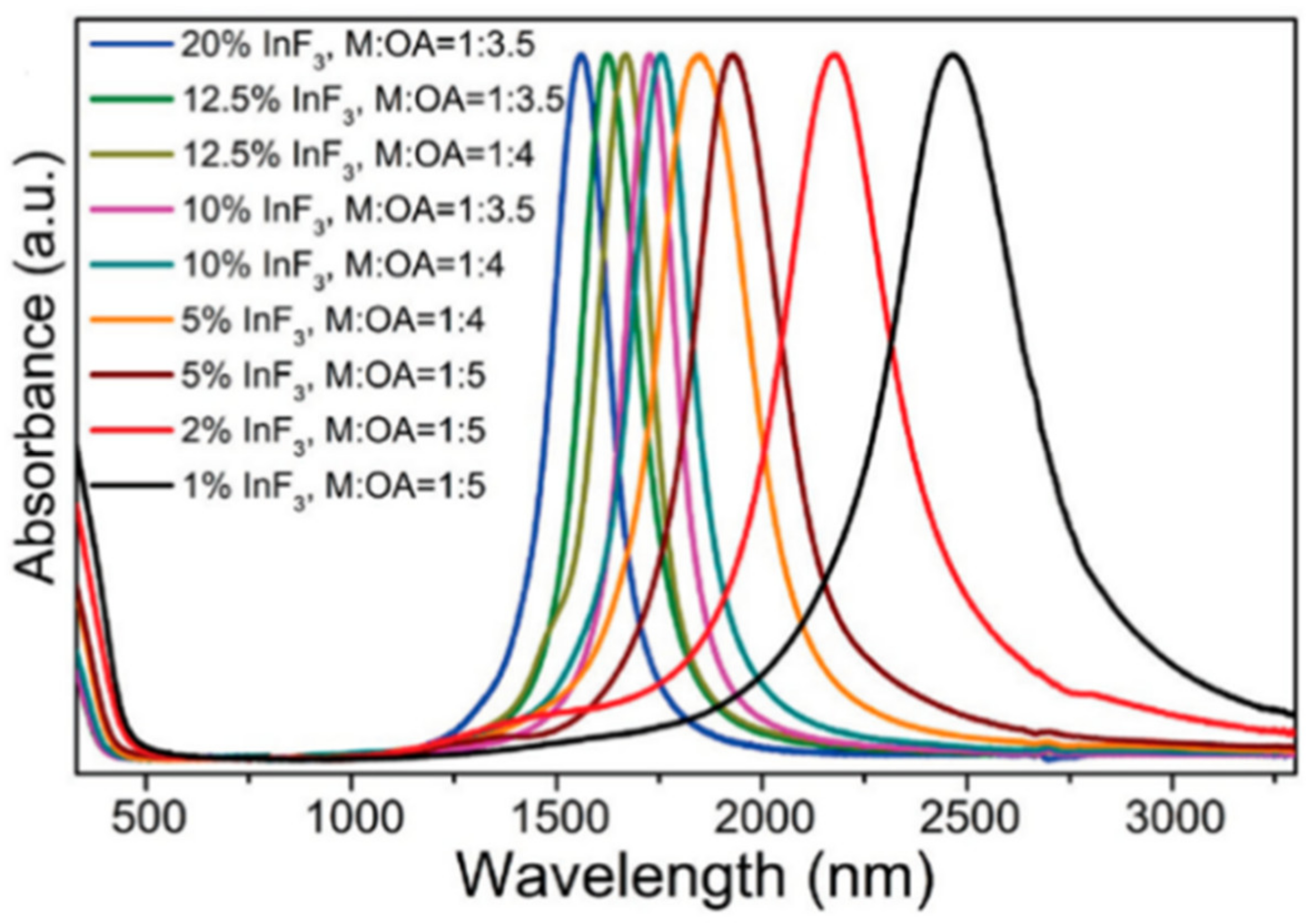
- Ye, X.; Fei, J.; Diroll, B.T.; Paik, T.; Murray, C.B. Expanding the Spectral Tunability of Plasmonic Resonances in Doped Metal-Oxide Nanocrystals through Cooperative Cation–Anion Codoping. J. Am. Chem. Soc. 2014, 136, 11680–11686. [Google Scholar] [CrossRef] [PubMed]
- Liu, Z.; Zhong, Y.; Shafei, I.; Borman, R.; Jeong, S.; Chen, J.; Losovyj, Y.; Gao, X.; Li, N.; Du, Y.; et al. Tuning infrared plasmon resonances in doped metal-oxide nanocrystals through cation-exchange reactions. Nat. Commun. 2019, 10, 1394. [Google Scholar] [CrossRef] [PubMed]
- Noginov, M.A.; Gu, L.; E Livenere, J.; Zhu, G.; Pradhan, A.K.; Mundle, R.; Bahoura, M.; Barnakov, Y.A.; A Podolskiy, V. Transparent conductive oxides: Plasmonic materials for telecom wavelengths. Appl. Phys. Lett. 2011, 99, 21101. [Google Scholar] [CrossRef]
- Al-Khamis, K.M.; Mahfouz, R.M.; Al-Warthan, A.A.; Siddiqui, M.R.H. Synthesis and characterization of gallium oxide nanoparticles. Arab. J. Chem. 2009, 2, 73–77. [Google Scholar] [CrossRef] [Green Version]
- Yarema, M.; Wörle, M.; Rossell, M.D.; Erni, R.; Caputo, R.; Protesescu, L.; Kravchyk, K.V.; Dirin, D.N.; Lienau, K.; Von Rohr, F.; et al. Monodisperse Colloidal Gallium Nanoparticles: Synthesis, Low Temperature Crystallization, Surface Plasmon Resonance and Li-Ion Storage. J. Am. Chem. Soc. 2014, 136, 12422–12430. [Google Scholar] [CrossRef]
- MacDonald, K.F.; Brocklesby, W.S.; Emelyanov, V.I.; Fedotov, V.A.; Pochon, S.; Ross, K.J.; Stevens, G.; Zheludev, N.I. Gallium nanoparticles grow where light is. arXiv 2001. arXiv preprint:physics/0105042. [Google Scholar]
- Nucciarelli, F.; Bravo, I.; Catalan-Gomez, S.; Vázquez, L.; Lorenzo, E.; Pau, J.L. High Ultraviolet Absorption in Colloidal Gallium Nanoparticles Prepared from Thermal Evaporation. Nanomaterials 2017, 7, 172. [Google Scholar] [CrossRef] [Green Version]
- Choi, S.-R.; Britigan, B.E.; Moran, D.M.; Narayanasamy, P. Gallium nanoparticles facilitate phagosome maturation and inhibit growth of virulent Mycobacterium tuberculosis in macrophages. PLoS ONE 2017, 12, e0177987. [Google Scholar] [CrossRef] [Green Version]
- Yu, F.; Xu, J.; Li, H.; Wang, Z.; Sun, L.; Deng, T.; Tao, P.; Liang, Q. Ga-In liquid metal nanoparticles prepared by physical vapor deposition. Prog. Nat. Sci. 2018, 28, 28–33. [Google Scholar] [CrossRef]
- Catalán-Gómez, S.; Bran, C.; Vázquez, M.; Pau, J.L.; Redondo-Cubero, A. Plasmonic coupling in closed-packed ordered gallium nanoparticles. Sci. Rep. 2020, 10, 1–11. [Google Scholar] [CrossRef] [Green Version]
- Marín, A.G.; García-Mendiola, T.; Bernabeu, C.N.; Hernández, M.J.; Piqueras, J.; Pau, J.L.; Pariente, F.; Lorenzo, E. Gallium plasmonic nanoparticles for label-free DNA and single nucleotide polymorphism sensing. Nanoscale 2016, 8, 9842–9851. [Google Scholar] [CrossRef] [Green Version]
- Soumya, K.; Selvam, I.P.; Potty, S. Study on the doping effect of spin coated Al and In doped and (Al/In) co-doped ZnO thin films for near-infrared plasmonic applications. Thin Solid Film. 2019, 687, 137482. [Google Scholar] [CrossRef]
- Tan, W.K.; Yokoi, A.; Kawamura, G.; Matsuda, A.; Muto, H. PMMA-ITO Composite Formation via Electrostatic Assembly Method for Infra-Red Filtering. Nanomaterials 2019, 9, 886. [Google Scholar] [CrossRef] [Green Version]
- Kanehara, M.; Koike, H.; Yoshinaga, T.; Teranishi, T. Indium Tin Oxide Nanoparticles with Compositionally Tunable Surface Plasmon Resonance Frequencies in the Near-IR Region. J. Am. Chem. Soc. 2009, 131, 17736–17737. [Google Scholar] [CrossRef] [PubMed]
- Lee, J.; Lee, S.; Li, G.; Petruska, M.A.; Paine, D.C.; Sun, S. A Facile Solution-Phase Approach to Transparent and Conducting ITO Nanocrystal Assemblies. J. Am. Chem. Soc. 2012, 134, 13410–13414. [Google Scholar] [CrossRef]
- Lounis, S.D.; Runnerstrom, E.L.; Bergerud, A.; Nordlund, D.; Milliron, D.J. Influence of Dopant Distribution on the Plasmonic Properties of Indium Tin Oxide Nanocrystals. J. Am. Chem. Soc. 2014, 136, 7110–7116. [Google Scholar] [CrossRef] [PubMed]
- Sakamoto, M.; Kawawaki, T.; Kimura, M.; Yoshinaga, T.; Vequizo, J.J.M.; Matsunaga, H.; Ranasinghe, C.S.K.; Yamakata, A.; Matsuzaki, H.; Furube, A.; et al. Clear and transparent nanocrystals for infrared-responsive carrier transfer. Nat. Commun. 2019, 10, 1–7. [Google Scholar] [CrossRef] [Green Version]
- Teranishi, T.; Eguchi, M.; Kanehara, M.; Gwo, S. Controlled localized surface plasmon resonance wavelength for conductive nanoparticles over the ultraviolet to near-infrared region. J. Mater. Chem. 2011, 21, 10238–10242. [Google Scholar] [CrossRef]
- Johns, R.W.; Bechtel, H.A.; Runnerstrom, E.L.; Agrawal, A.; Lounis, S.D.; Milliron, D.J. Direct observation of narrow mid-infrared plasmon linewidths of single metal oxide nanocrystals. Nat. Commun. 2016, 7, 11583. [Google Scholar] [CrossRef] [PubMed]
- Li, S.Q.; Guo, P.; Zhang, L.; Zhou, W.; Odom, T.W.; Seideman, T.; Ketterson, J.B.; Chang, R.P.H. Infrared Plasmonics with Indium–Tin-Oxide Nanorod Arrays. ACS Nano 2011, 5, 9161–9170. [Google Scholar] [CrossRef] [PubMed]
- Li, Z.; Zhang, Z.; Chen, K. Indium–Tin–Oxide Nanostructures for Plasmon-Enhanced Infrared Spectroscopy: A Numerical Study. Micromachines 2019, 10, 241. [Google Scholar] [CrossRef] [Green Version]
- Dar, G.I.; Saeed, M.; Wu, A. Toxicity of TiO2 Nanoparticles. In TiO2 Nanoparticles; Wiley: Hoboken, NJ, USA, 2020; pp. 67–103. [Google Scholar]
- Manthiram, K.; Alivisatos, A.P. Tunable Localized Surface Plasmon Resonances in Tungsten Oxide Nanocrystals. J. Am. Chem. Soc. 2012, 134, 3995–3998. [Google Scholar] [CrossRef] [PubMed]
- Rini, M.; Cavalleri, A.; Schoenlein, R.W.; Lopez, R.; Feldman, L.C.; Haglund, R.F.; Boatner, L.A.; Haynes, T.E. Photoinduced phase transition in VO_2 nanocrystals: Ultrafast control of surface-plasmon resonance. Opt. Lett. 2005, 30, 558–560. [Google Scholar] [CrossRef] [PubMed]
- Ghosh, S.; Lu, H.-C.; Cho, S.H.; Maruvada, T.; Price, M.C.; Milliron, D.J. Colloidal ReO3 Nanocrystals: Extra Re d-Electron Instigating a Plasmonic Response. J. Am. Chem. Soc. 2019, 141, 16331–16343. [Google Scholar] [CrossRef] [PubMed]
- Guo, T.; Yao, M.-S.; Lin, Y.-H.; Nan, C.-W. A comprehensive review on synthesis methods for transition-metal oxide nanostructures. CrystEngComm 2015, 17, 3551–3585. [Google Scholar] [CrossRef]
- Matsui, H.; Furuta, S.; Tabata, H. Role of electron carriers on local surface plasmon resonances in doped oxide semiconductor nanocrystals. Appl. Phys. Lett. 2014, 104, 211903. [Google Scholar] [CrossRef]
- Sweatlock, L.A.; Diest, K. Vanadium dioxide based plasmonic modulators. Opt. Express 2012, 20, 8700–8709. [Google Scholar] [CrossRef]
- Ding, S.; Liu, Z.; Li, D.; Zhao, W.; Wang, Y.; Wan, D.; Huang, F. Tunable Assembly of Vanadium Dioxide Nanoparticles to Create Porous Film for Energy-Saving Applications. ACS Appl. Mater. Interfaces 2013, 5, 1630–1635. [Google Scholar] [CrossRef] [PubMed]
- Zomaya, D.; Xu, W.Z.; Grohe, B.; Mittler, S.; Charpentier, P.A. Bimodal Size Distribution of VO2 Nanoparticles in Hydrophilic Polymer Films for Temperature-Triggered Infrared Transmission Control. ACS Appl. Nano Mater. 2020, 3, 6645–6653. [Google Scholar] [CrossRef]
- Jostmeier, T.; Mangold, M.; Zimmer, J.; Karl, H.; Krenner, H.J.; Ruppert, C.; Betz, M. Thermochromic modulation of surface plasmon polaritons in vanadium dioxide nanocomposites. Opt. Express 2016, 24, 17321–17331. [Google Scholar] [CrossRef] [PubMed] [Green Version]
- Xi, W.-S.; Song, Z.-M.; Chen, Z.; Chen, N.; Yan, G.-H.; Gao, Y.; Cao, A.; Liu, Y.; Wang, H. Short-term and long-term toxicological effects of vanadium dioxide nanoparticles on A549 cells. Environ. Sci. Nano 2019, 6, 565–579. [Google Scholar] [CrossRef]
- Fang, B.; Li, Y.; Tong, G.; Wang, X.; Yan, M.; Liang, Q.; Wang, F.; Qin, Y.; Ding, J.; Chen, S.; et al. Optical properties of vanadium dioxide thin film in nanoparticle structure. Opt. Mater. 2015, 47, 225–230. [Google Scholar] [CrossRef]
- Nag, J.; Haglund, R.F., Jr. Synthesis of vanadium dioxide thin films and nanoparticles. J. Phys. Condens. Matter 2008, 20. [Google Scholar] [CrossRef]
- Liang, J.; Li, P.; Song, X.; Zhou, L. The fabrication and visible–near-infrared optical modulation of vanadium dioxide/silicon dioxide composite photonic crystal structure. Appl. Phys. A 2017, 123, 794. [Google Scholar] [CrossRef]
- Xu, G.; Huang, C.-M.; Tazawa, M.; Jin, P.; Chen, L.-H. Tunable optical properties of nano-Au on vanadium dioxide. Opt. Commun. 2009, 282, 896–902. [Google Scholar] [CrossRef]
- Xu, G.; Chen, Y.; Tazawa, M.; Jin, P. Surface Plasmon Resonance of Silver Nanoparticles on Vanadium Dioxide. J. Phys. Chem. B 2006, 110, 2051–2056. [Google Scholar] [CrossRef] [PubMed]
- Amekura, H.; Nakayama, Y.; Mitsuishi, K.; Kono, K. Formation of metallic vanadium nanoparticles in SiO2 by ion implantation and of vanadium oxide nanoparticles by additional thermal oxidation. Thin Solid Film. 2012, 520, 5528–5533. [Google Scholar] [CrossRef]


Publisher’s Note: MDPI stays neutral with regard to jurisdictional claims in published maps and institutional affiliations. |
© 2021 by the authors. Licensee MDPI, Basel, Switzerland. This article is an open access article distributed under the terms and conditions of the Creative Commons Attribution (CC BY) license (http://creativecommons.org/licenses/by/4.0/).
Share and Cite
S. S. dos Santos, P.; M. M. M. de Almeida, J.; Pastoriza-Santos, I.; C. C. Coelho, L. Advances in Plasmonic Sensing at the NIR—A Review. Sensors 2021, 21, 2111. https://doi.org/10.3390/s21062111
S. S. dos Santos P, M. M. M. de Almeida J, Pastoriza-Santos I, C. C. Coelho L. Advances in Plasmonic Sensing at the NIR—A Review. Sensors. 2021; 21(6):2111. https://doi.org/10.3390/s21062111
Chicago/Turabian StyleS. S. dos Santos, Paulo, José M. M. M. de Almeida, Isabel Pastoriza-Santos, and Luís C. C. Coelho. 2021. "Advances in Plasmonic Sensing at the NIR—A Review" Sensors 21, no. 6: 2111. https://doi.org/10.3390/s21062111
APA StyleS. S. dos Santos, P., M. M. M. de Almeida, J., Pastoriza-Santos, I., & C. C. Coelho, L. (2021). Advances in Plasmonic Sensing at the NIR—A Review. Sensors, 21(6), 2111. https://doi.org/10.3390/s21062111