
Universal Filter Based on Compact CMOS Structure of VDDDA


Abstract
1. Introduction
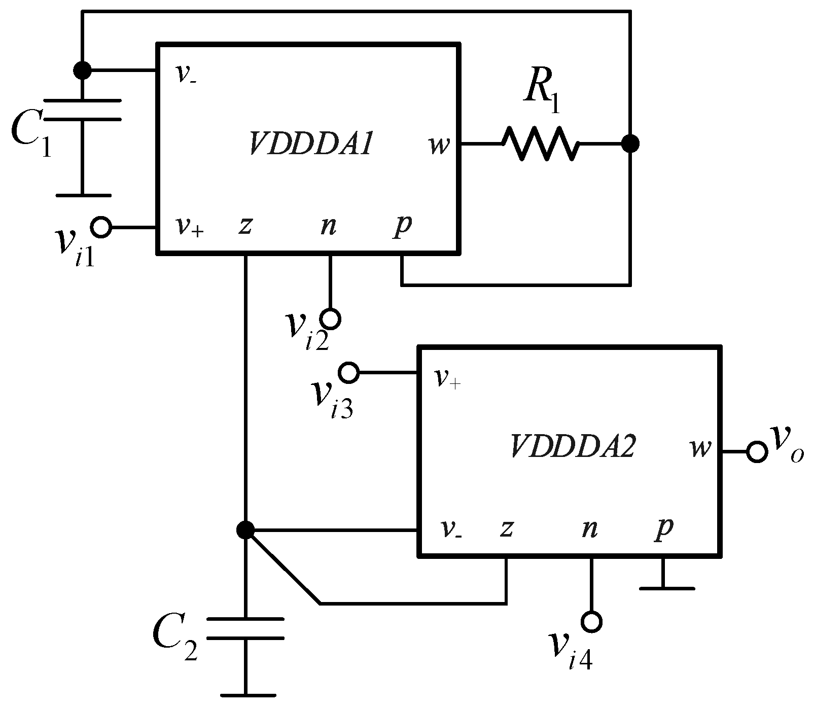
2. Proposed Universal Filter
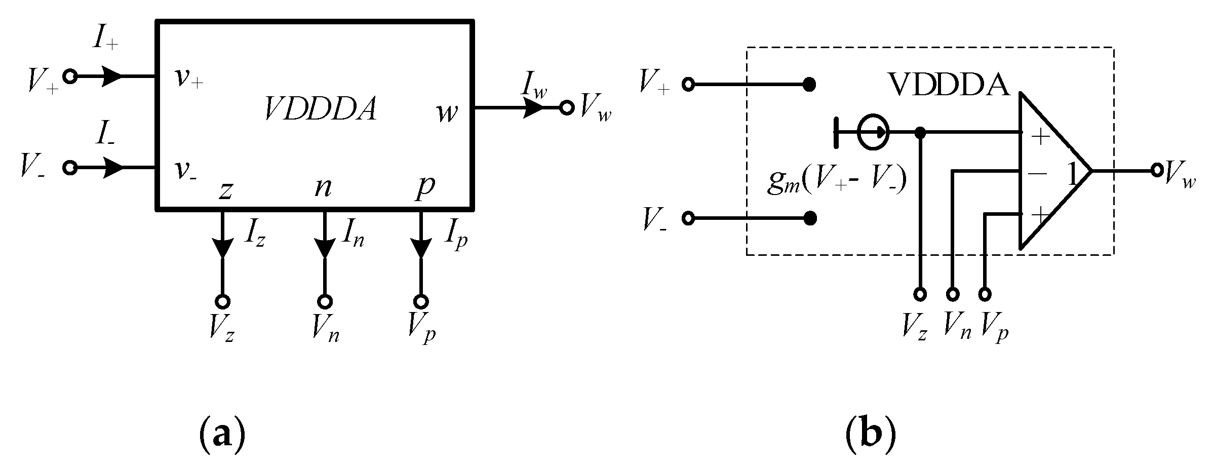
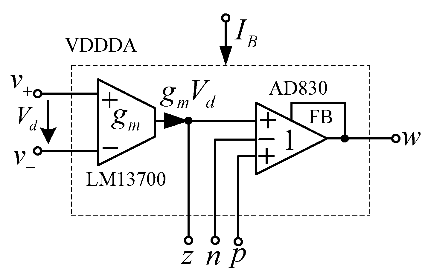
2.1. Basic Concept of the VDDDA
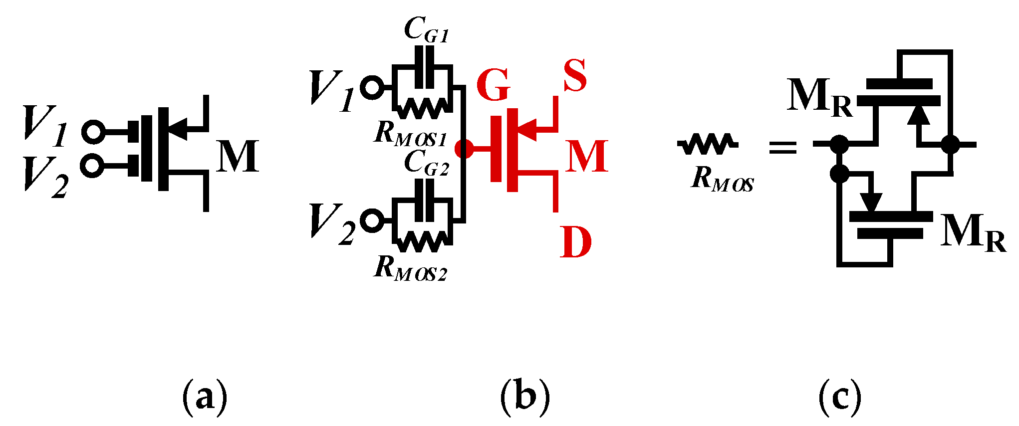
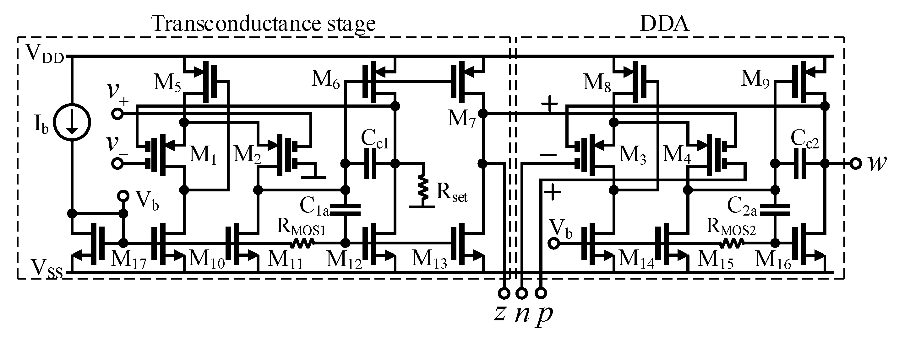
2.2. The CMOS Structure of the VDDDA
2.3. The Universal Biquad Filter based on VDDDAs
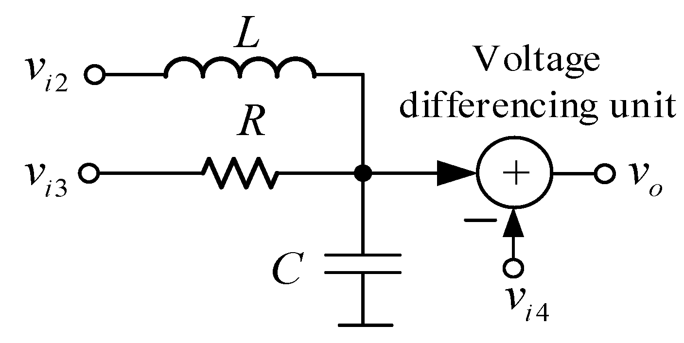
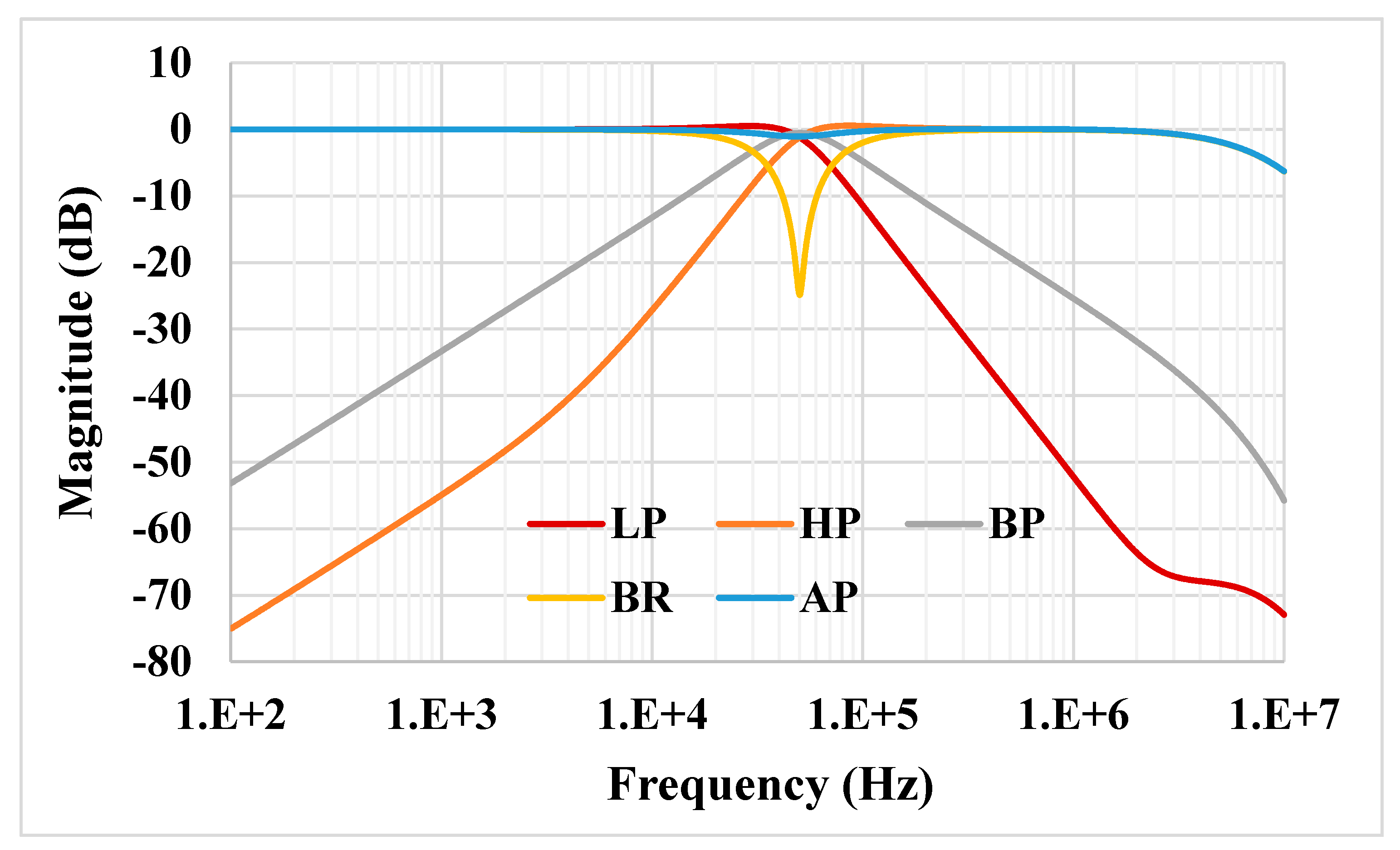
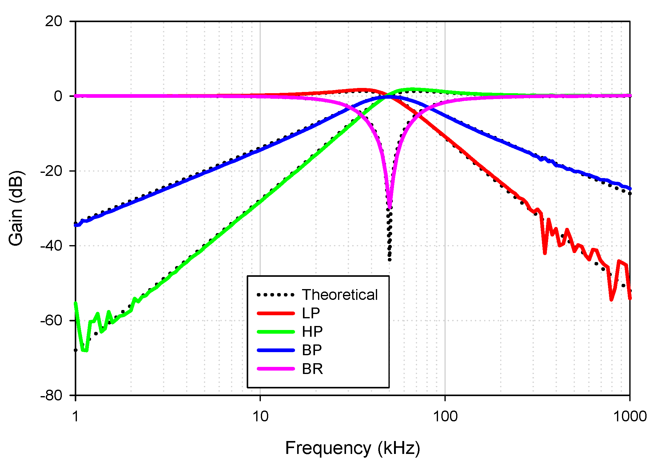
- Noninverting low-pass filter with unity voltage gain is given at the output voltage node vo of the proposed filter by applying the input signal into the input voltage node vi2 while the other input voltage nodes are grounded.
- Noninverting band-pass filter with unity voltage gain is given at the output voltage node vo of the proposed filter by applying the input signal into the input voltage node vi3 while the other input voltage nodes are grounded.
- Inverted high-pass filter with unity voltage gain is given at the output voltage node vo of the proposed filter by applying the input signal into the input voltage nodes vi2, vi3 and vi4 while the input voltage node vi1 is grounded.
- Inverted band-stop filter with unity voltage gain is given at the output voltage node vo of the proposed filter by applying the input signal into the input voltage nodes vi3 and vi4 while other nodes are grounded.
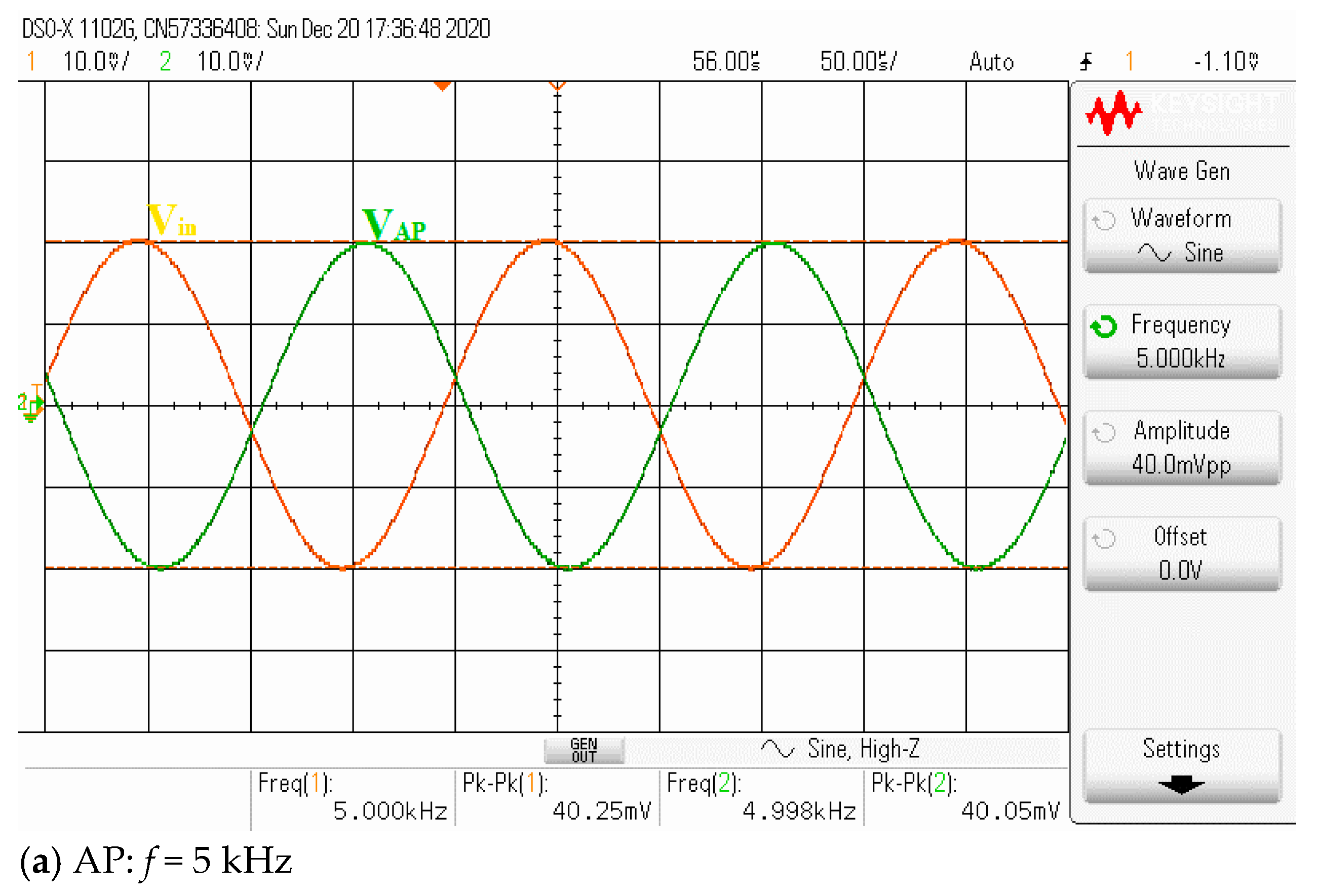
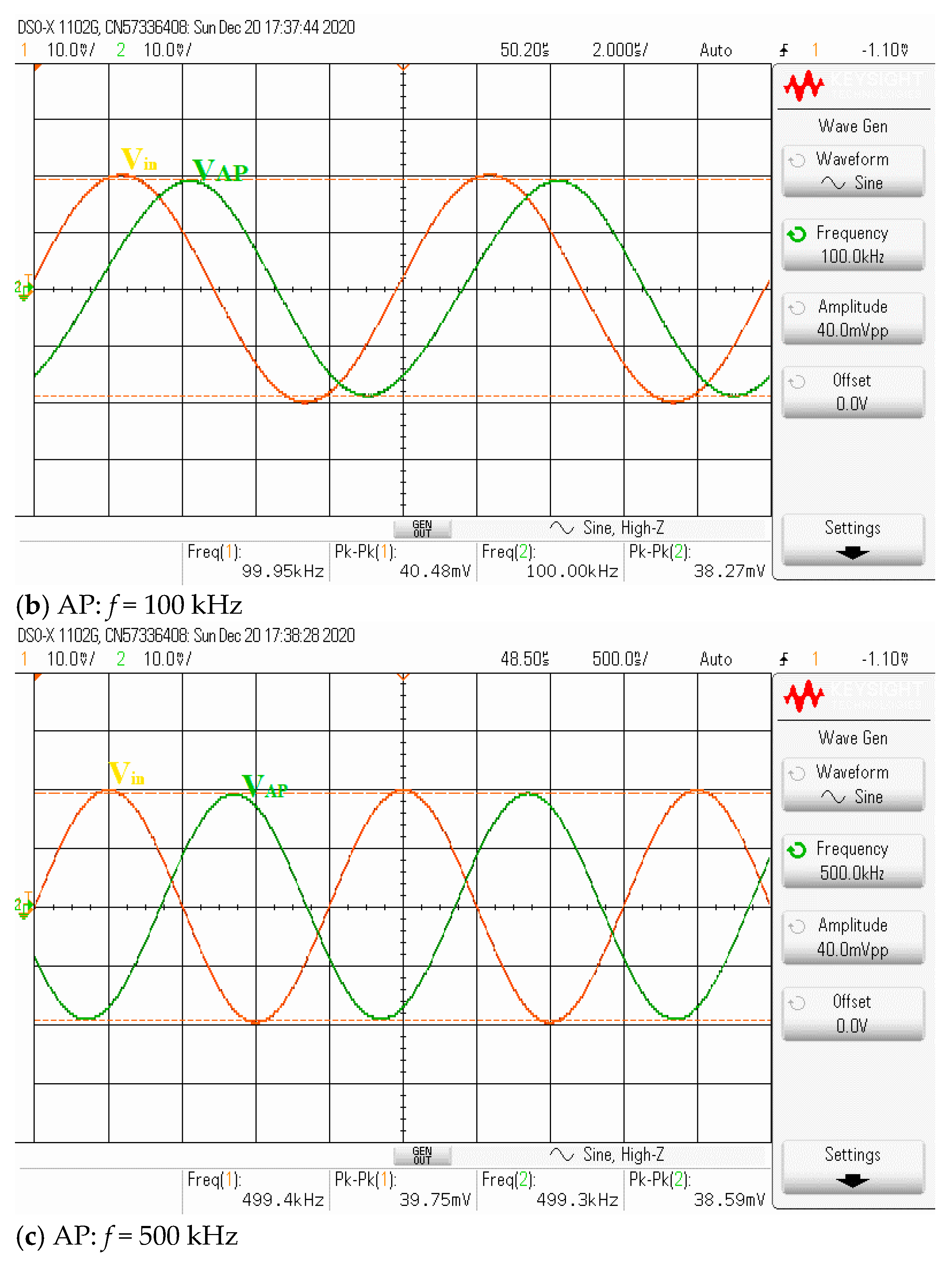
- Inverted all-pass filter with unity voltage gain is given at the output voltage node vo of the proposed filter by setting gm1 = gm2 and applying the input signal into the input voltage nodes vi1, vi3 and vi4 while the input voltage node vi2 is grounded. Although it requires the matching conditions of gm1 and gm2, this is the active matching condition that is easier to control than the passive matching one.
- Inverted all-pass filter without the matching condition is given at the output voltage node vo of the proposed filter by connecting the z terminal to the p terminal of the VDDDA2, then applying the input signal into the input volage nodes vi3 and vi4 while the other input voltage nodes are grounded.
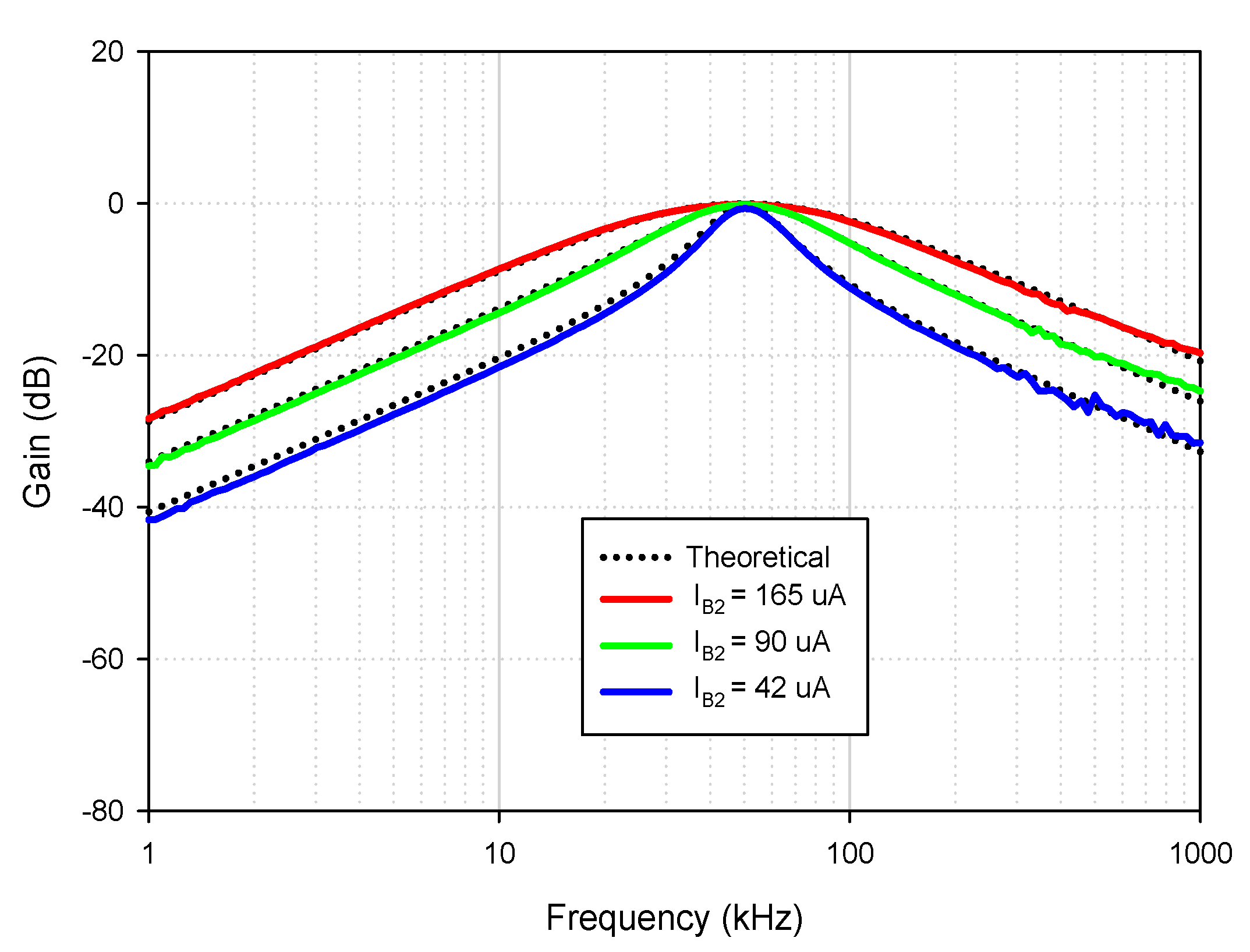
2.4. Effects of Nonideal VDDDA Characteristics
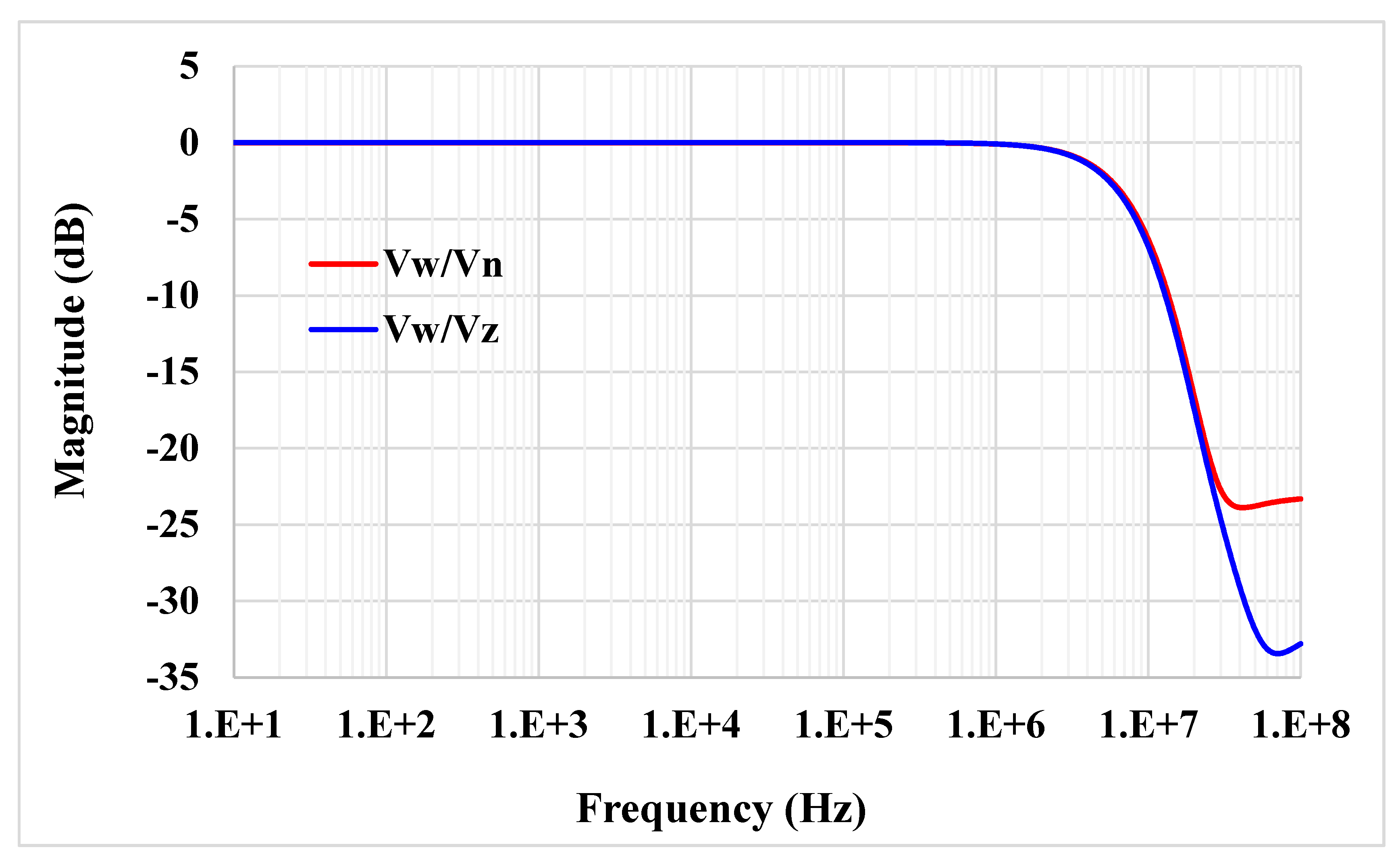
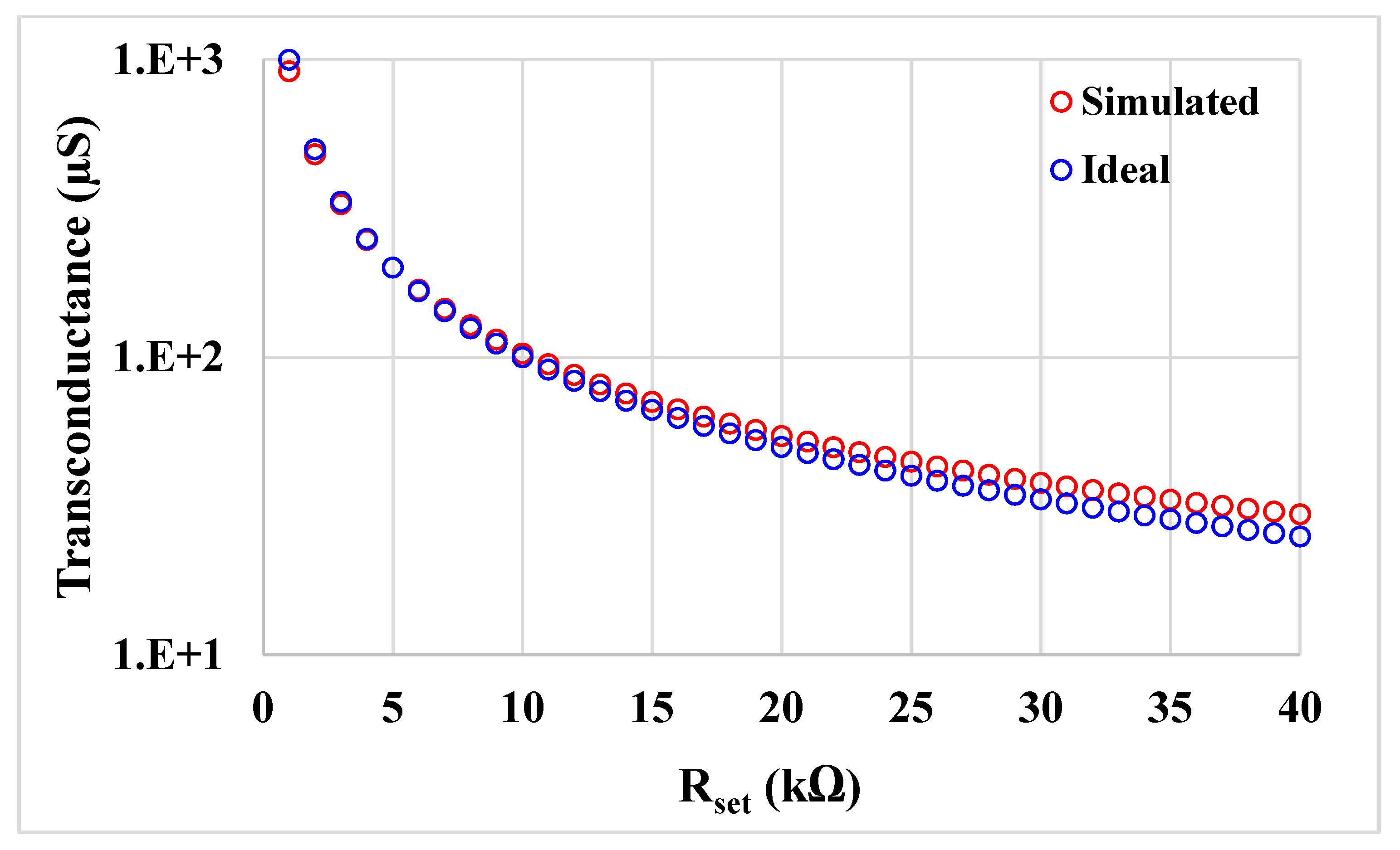
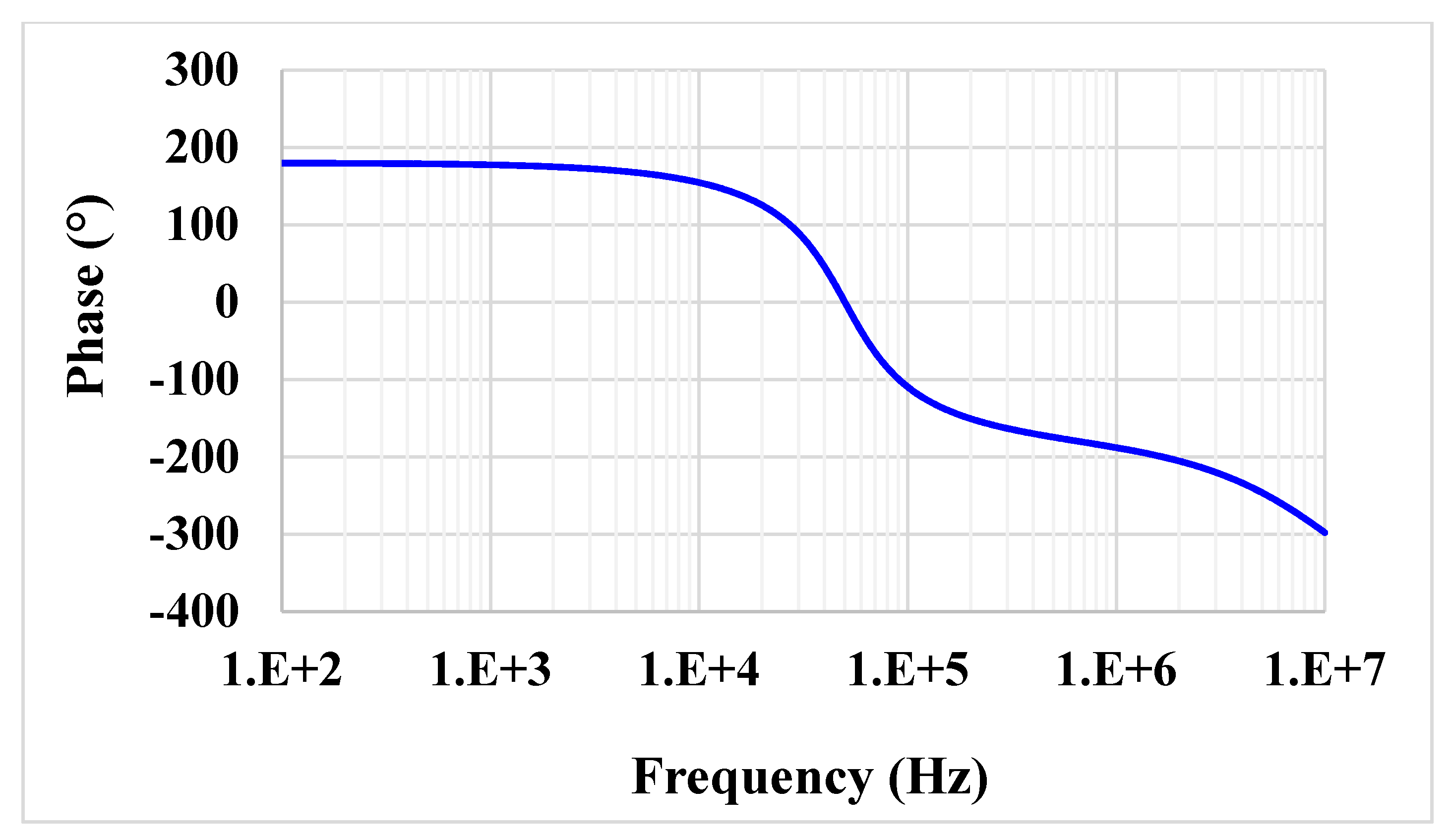
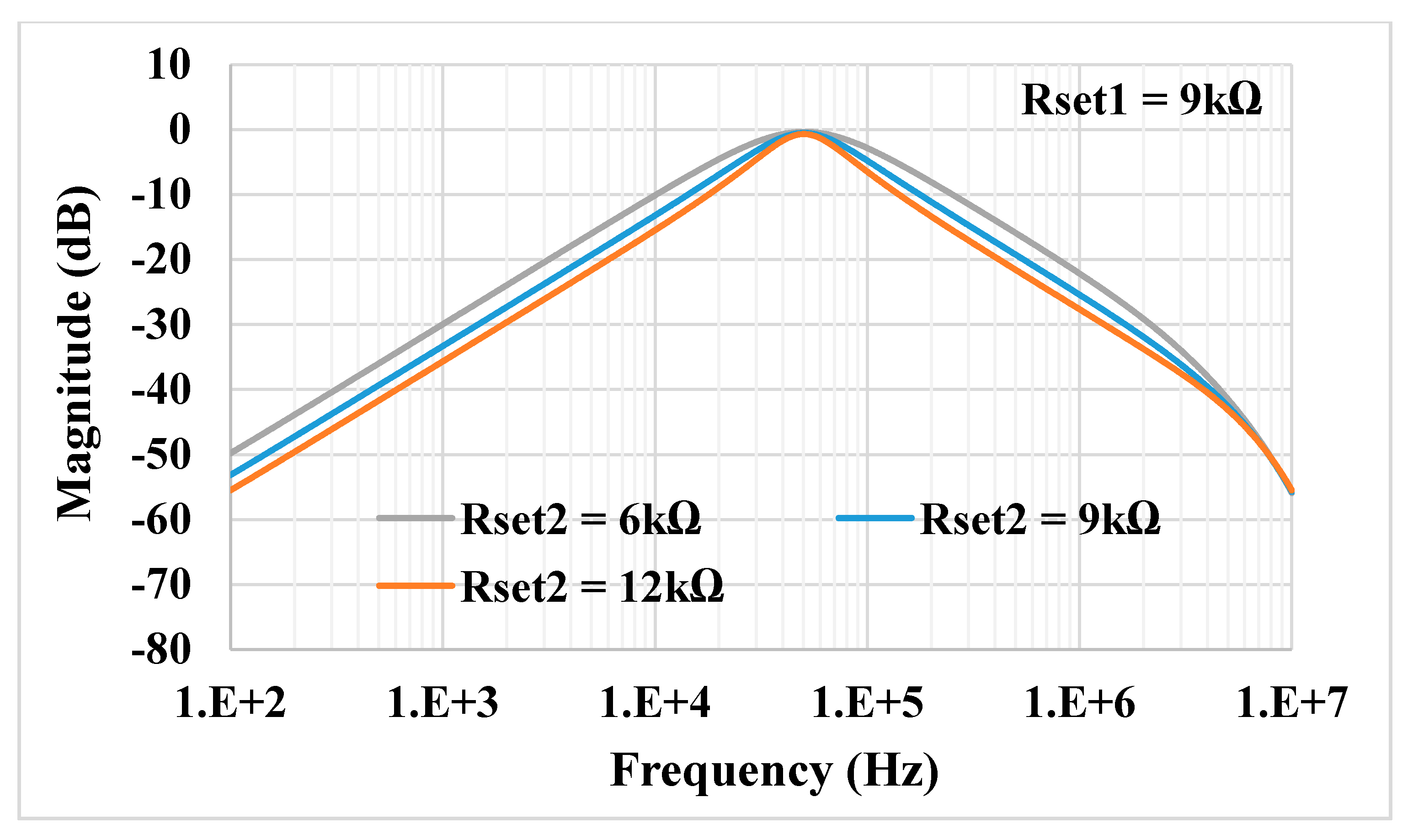
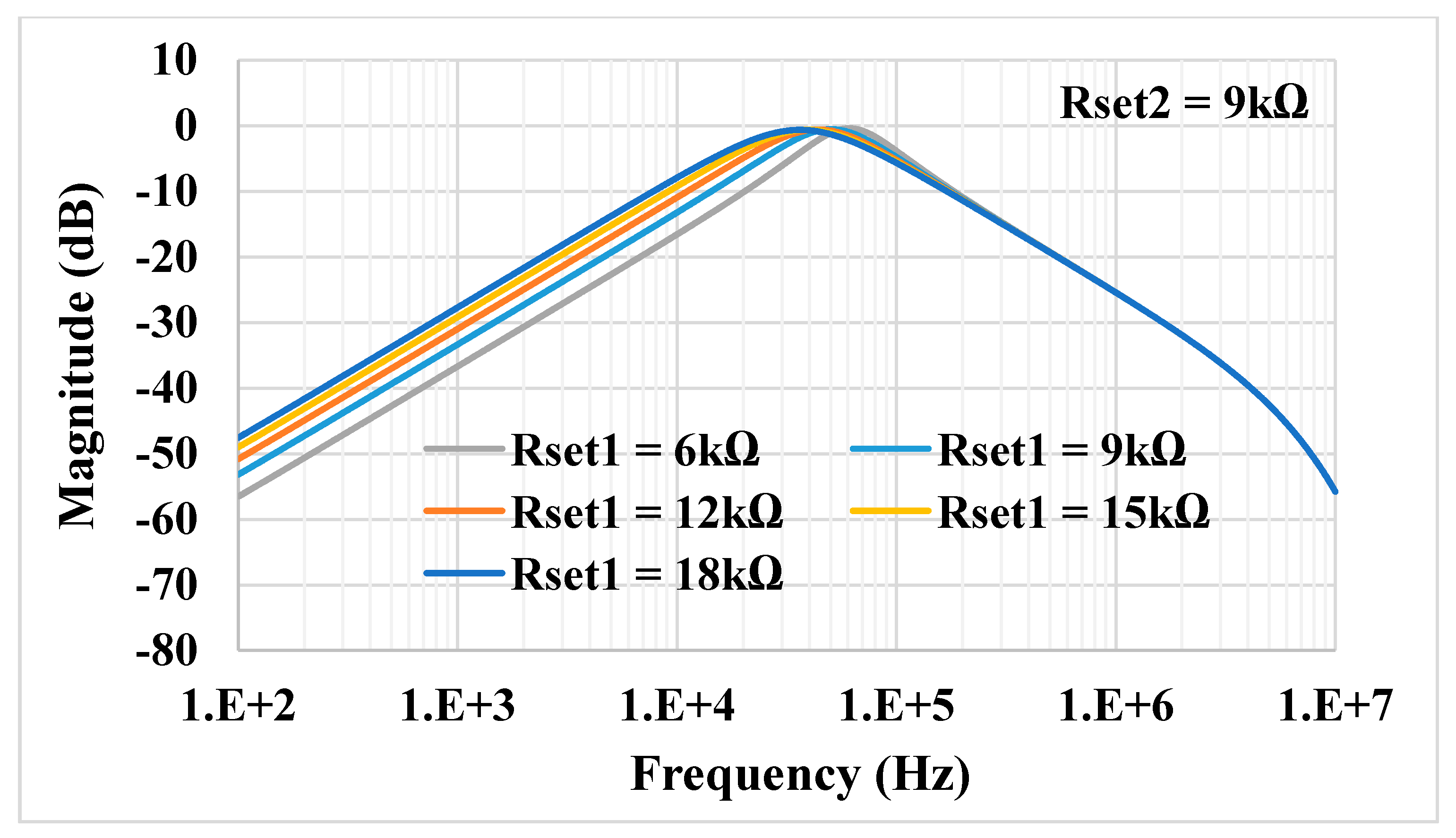
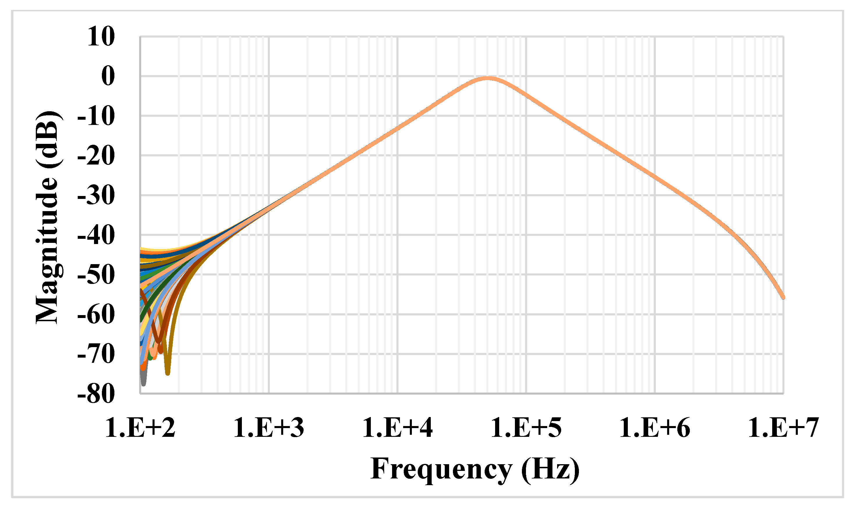
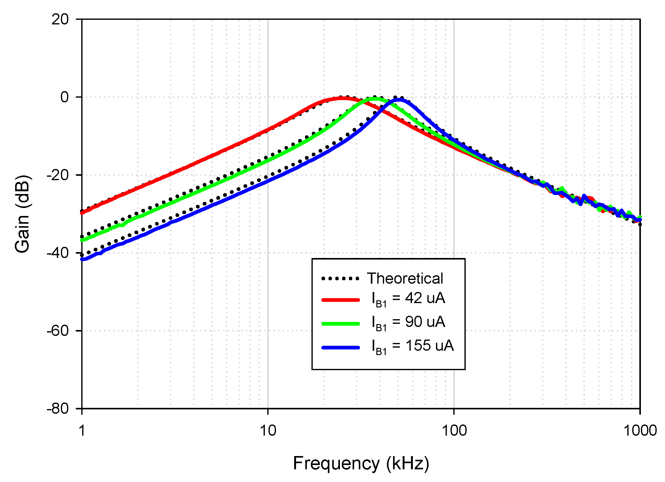
3. Simulation Results
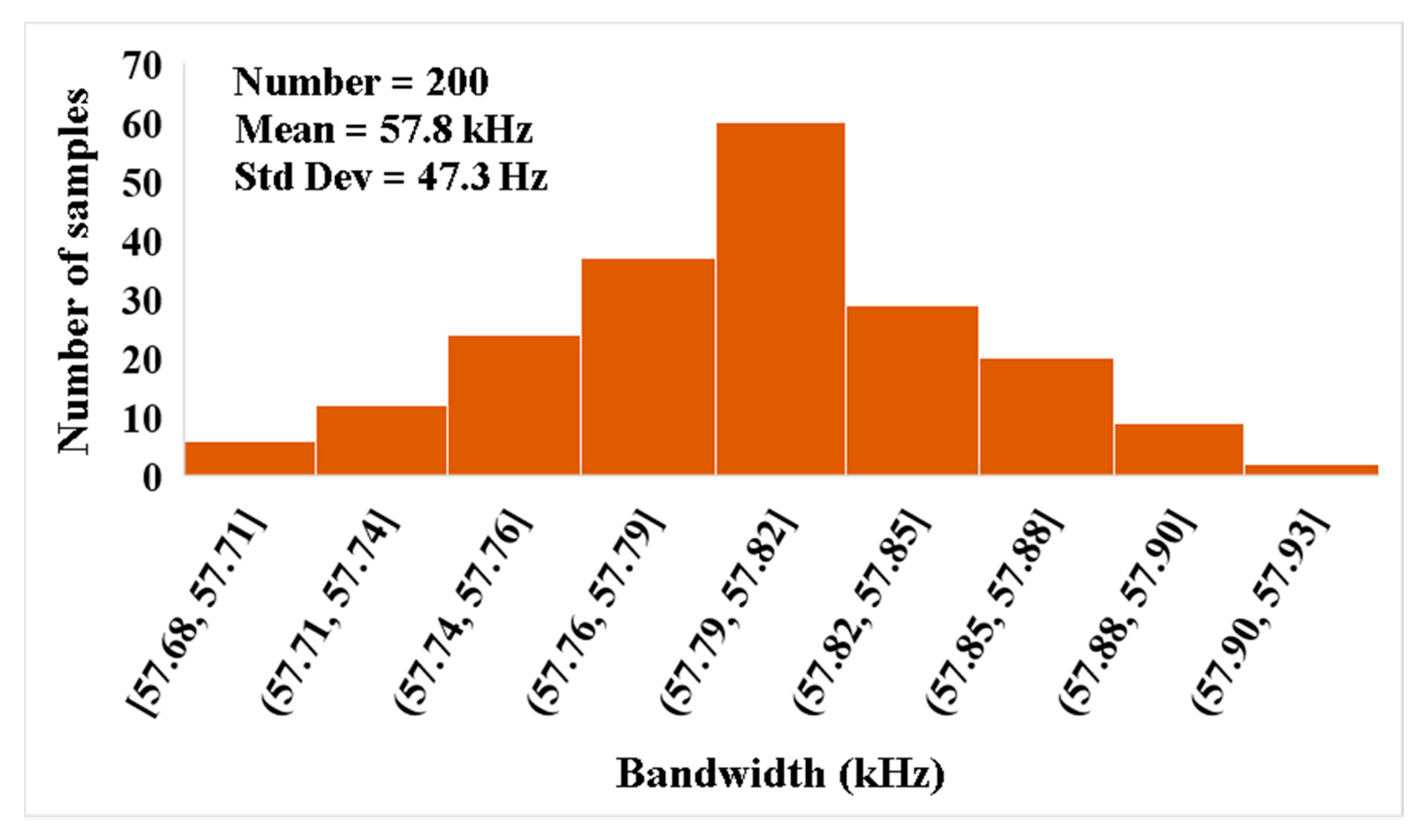
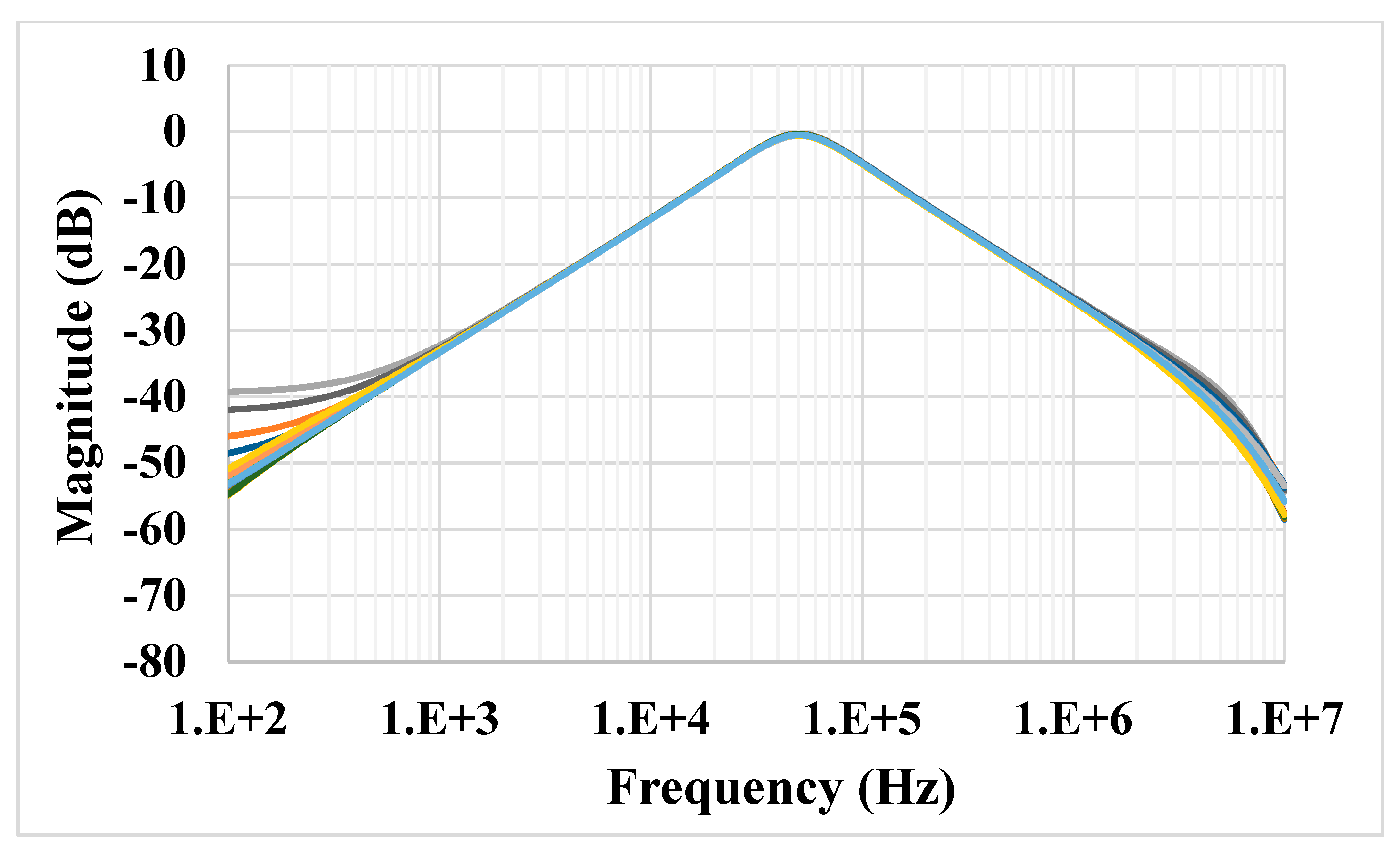
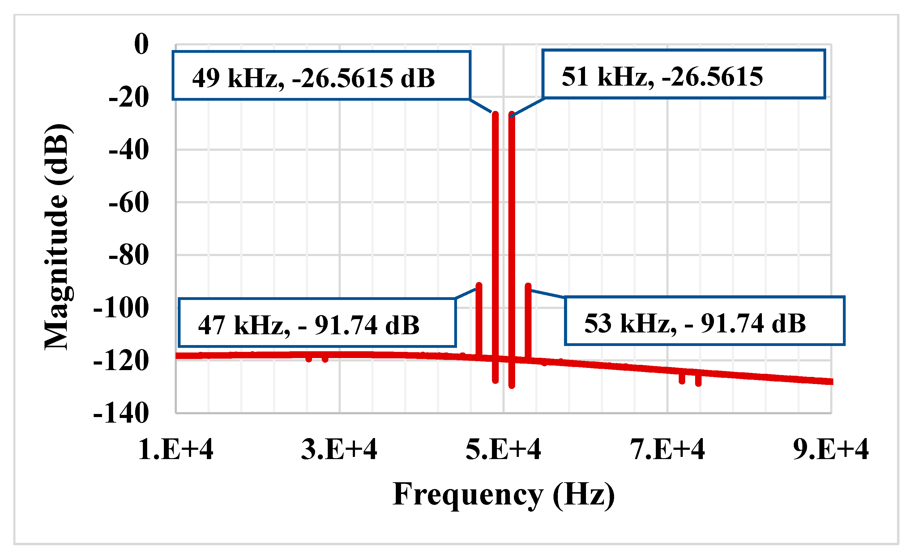
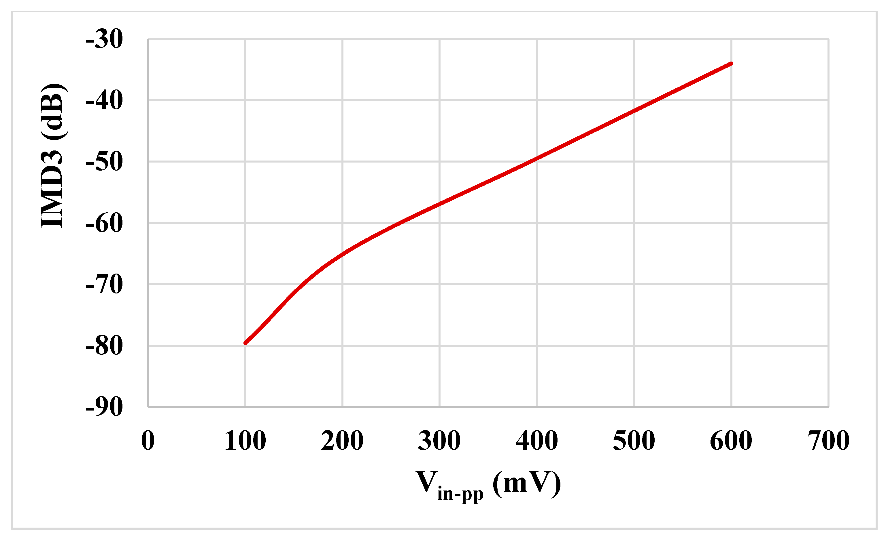
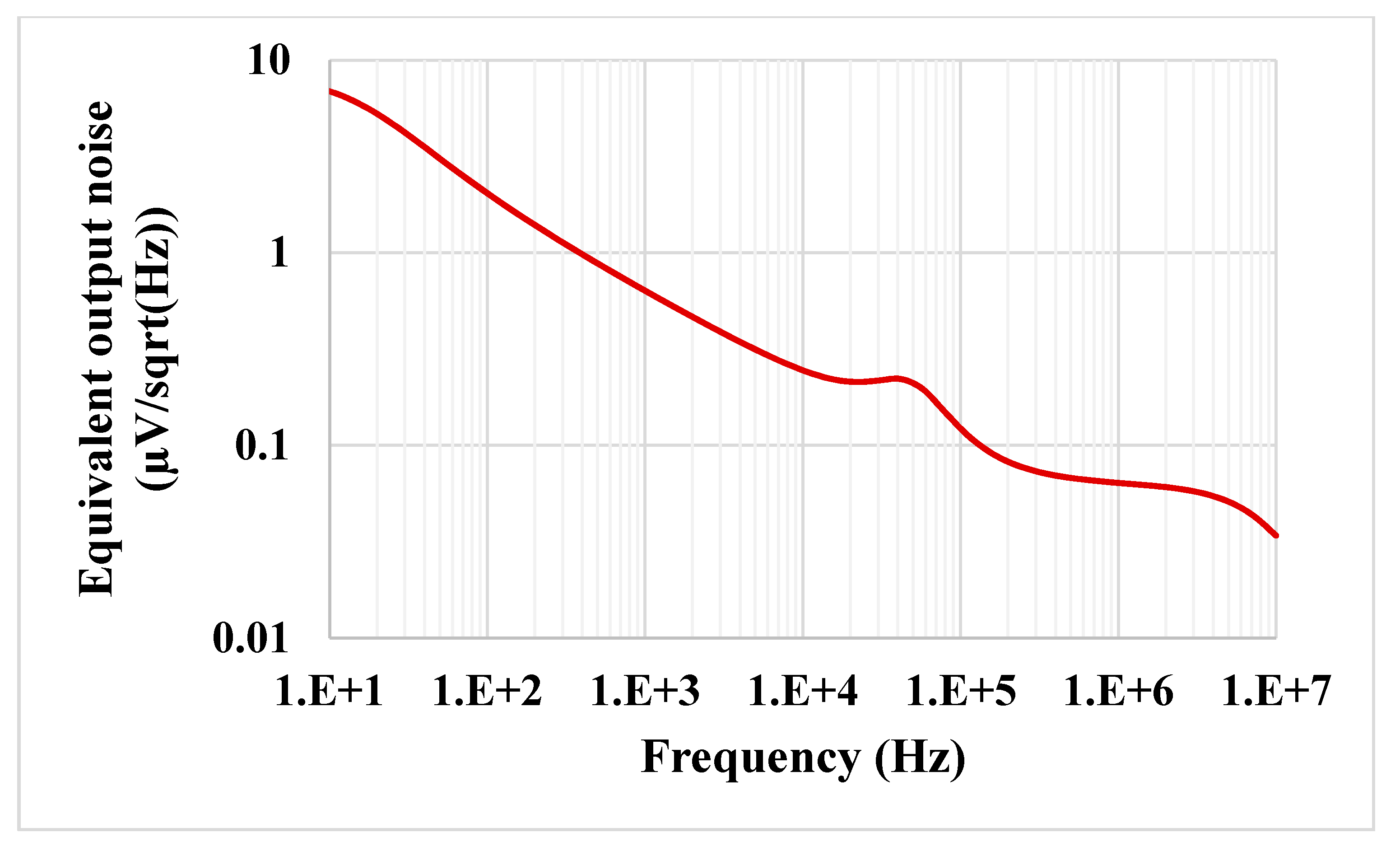
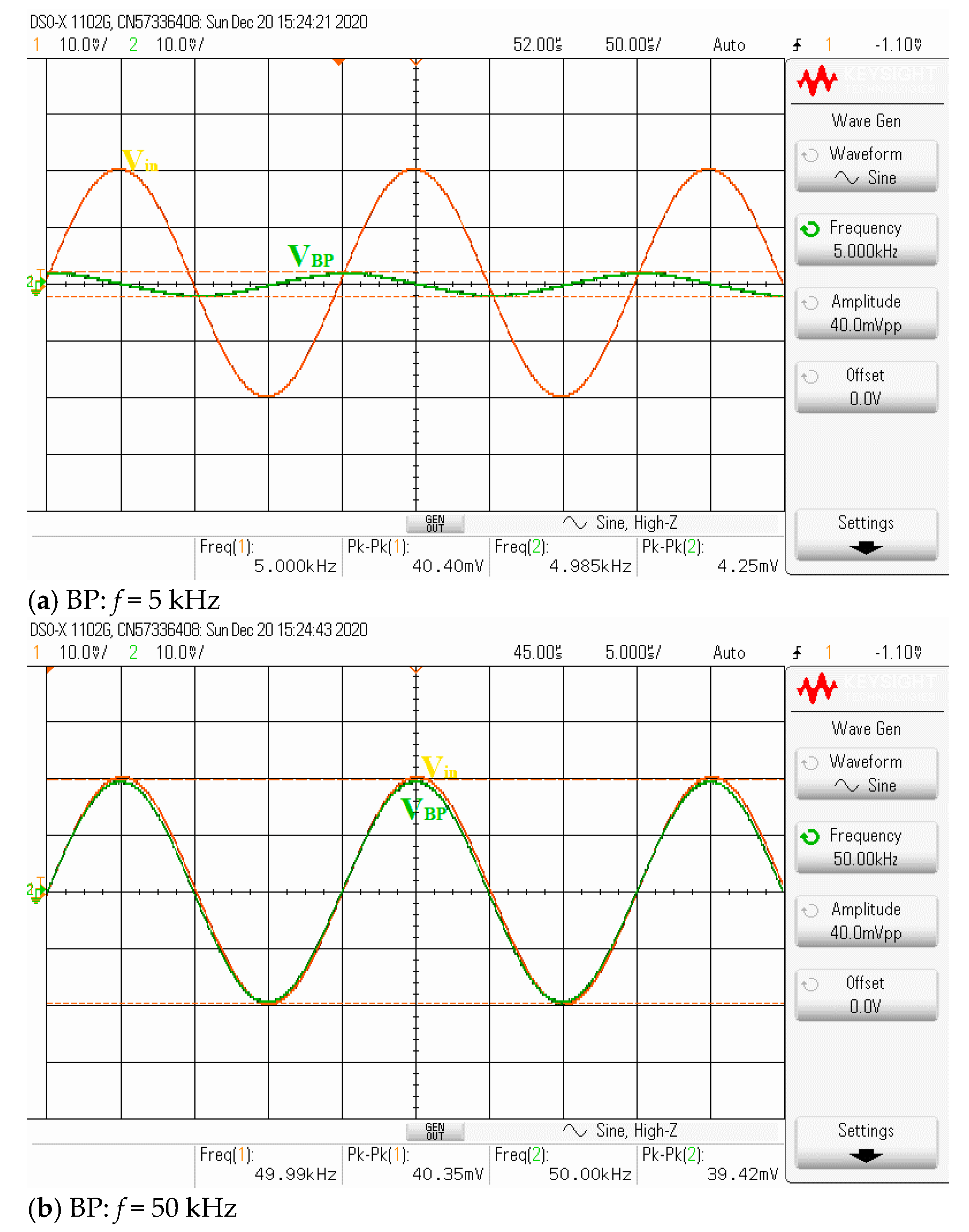
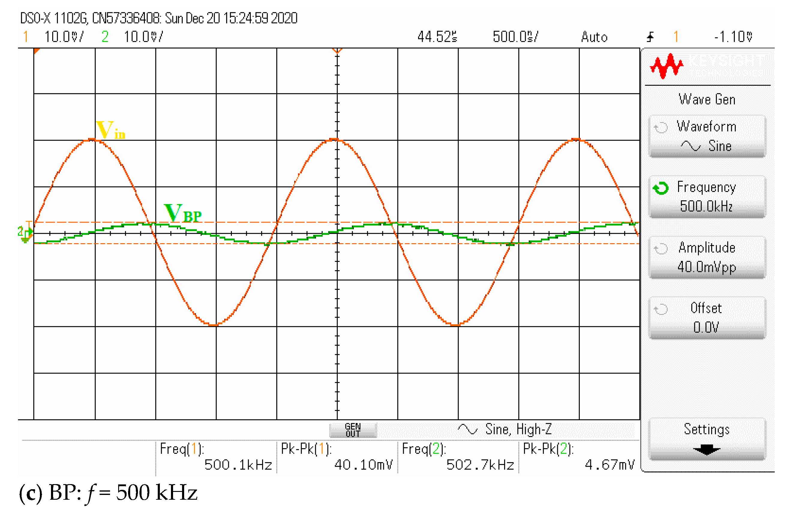
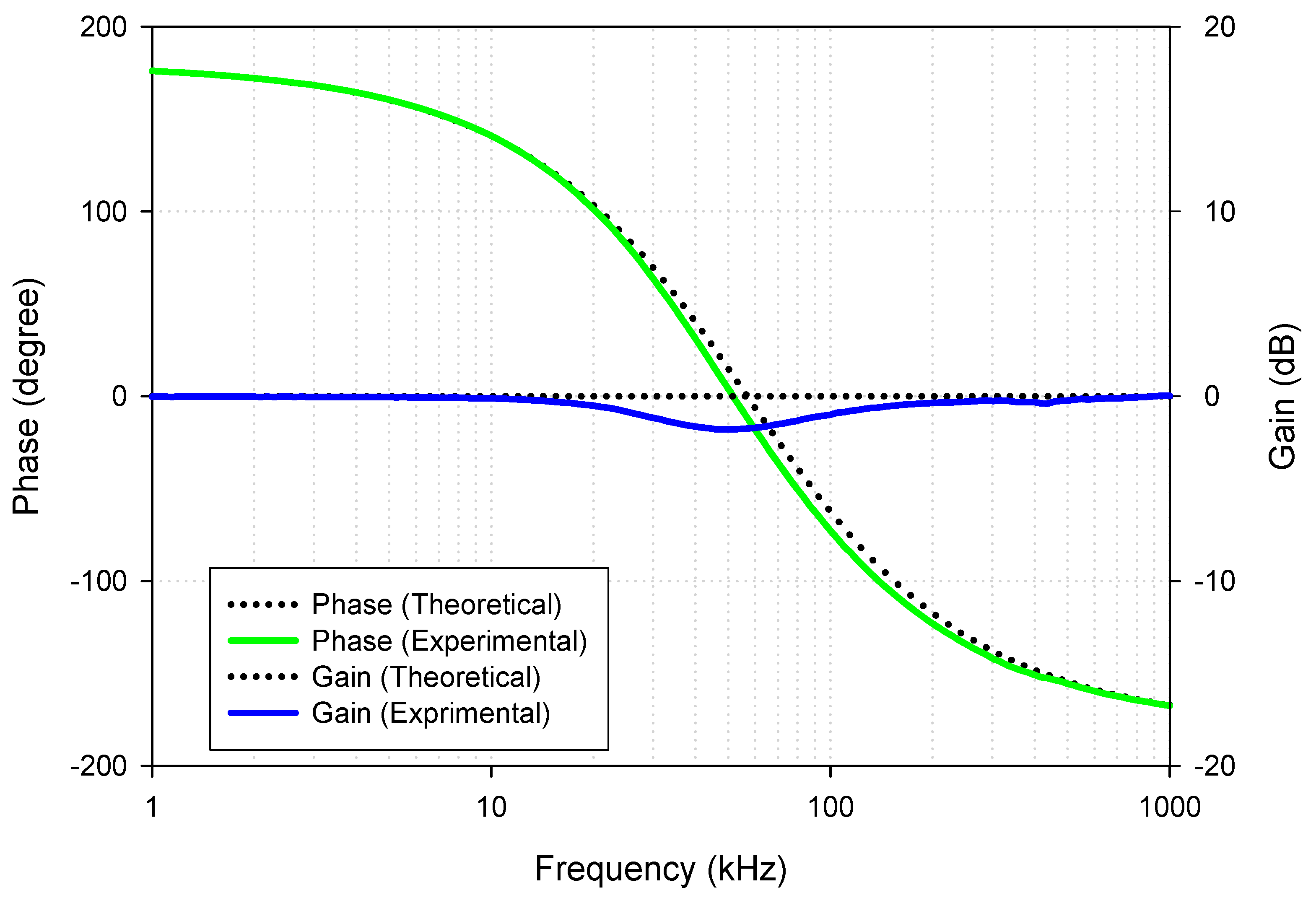
4. Experimental Results
5. Comparison
6. Conclusions
Author Contributions
Funding
Acknowledgments
Conflicts of Interest
References
- Myderrizi, I.; Minaei, M.; Yuce, E. An Electronically Fine-Tunable Multi-Input-Single-Output Universal Filter. IEEE Trans. Biomed. Circuits Syst. II Express Briefs 2011, 58, 356–360. [Google Scholar] [CrossRef]
- Psychalinos, C. Log-domain SIMO and MISO low-voltage universal biquads. Analog Integr. Circuits Signal Process. 2011, 67, 201–211. [Google Scholar] [CrossRef]
- Yuce, E.; Tez, S. A Novel Voltage-Mode Universal Filter Composed of Two Terminal Active Devices. AEU Int. J. Electron. Commun. 2018, 86, 202–209. [Google Scholar] [CrossRef]
- Ballo, A.; Grasso, A.D.; Pennisi, S.; Venezia, C. High-Frequency Low-Current Second-Order Bandpass Active Filter Topology and Its Design in 28-nm FD-SOI CMOS. J. Low Power Electron. Appl. 2020, 10, 27. [Google Scholar] [CrossRef]
- Wang, S.F.; Chen, H.P.; Ku, Y.; Zhong, M.X. Voltage-mode multifunction biquad filter and its application as fully-uncoupled quadrature oscillator based on current-feedback operational amplifiers. Sensors 2020, 20, 6681. [Google Scholar] [CrossRef] [PubMed]
- Kumngern, M.; Aupithak, N.; Khateb, F.; Kulej, T. 0.5 V Fifth-Order Butterworth Low-Pass Filter Using Multiple-Input OTA for ECG Applications. Sensors 2020, 20, 7343. [Google Scholar] [CrossRef]
- Prommee, P.; Wongprommoon, N.; Kumngern, M.; Jaikla, W. Low-voltage low-pass and band-pass elliptic filters based on log-domain approach suitable for biosensors. Sensors 2019, 19, 5581. [Google Scholar] [CrossRef]
- Alpaslan, H.; Yuce, E. DVCC+ based multifunction and universal filters with the high input impedance features. Analog Integr. Circuits Signal Process. 2020, 103, 325–335. [Google Scholar] [CrossRef]
- Safari, L.; Barile, G.; Ferri, G.; Stornelli, V. A new low-voltage low-power dual-mode VCII-based simo universal filter. Electronics 2019, 8, 765. [Google Scholar] [CrossRef]
- Psychalinos, C.; Kasimis, C.; Khateb, F. Multiple-input single-output universal biquad filter using single output operational transconductance amplifiers. AEU Int. J. Electron. Commun. 2018, 93, 360–367. [Google Scholar] [CrossRef]
- Pandey, N.; Nand, D.; Khan, Z. Single-Input Four-Output Current Mode Filter Using Operational Floating Current Conveyor. Act. Passiv. Electron. Compon. 2013, 2013, 318560. [Google Scholar] [CrossRef]
- Minaei, S.; Yuce, E. All-Grounded Passive Elements Voltage-Mode DVCC-Based Universal Filters. Circuits Syst. Signal Process. 2010, 29, 295–309. [Google Scholar] [CrossRef]
- Koton, J.; Herencsar, N.; Vrba, K.; Metin, B. The VDDDA in multifunction filter with mutually independent Q and ω0 control feature. In Proceedings of the 8th International Conference on Electrical and Electronics Engineering, Bursa, Turkey, 28–30 November 2013; pp. 53–56. [Google Scholar]
- Koton, J.; Herencsar, N.; Vrba, K.; Metin, B. Voltage-mode multifunction filter with mutually independent Q and control feature using VDDDAs. Analog Integr. Circuits Signal Process. 2014, 81, 53–60. [Google Scholar] [CrossRef]
- Soisang, S.; Jirasereemomkul, K.; Jaikla, W.; Higuchi, K. Voltage-Mode Multifunctional Biquadratic Filter Using VDDDA. Appl. Mech. Mater. 2015, 781, 155–159. [Google Scholar] [CrossRef]
- Siripongdee, S.; Jaikla, W. Single VDDDA-based voltage-mode multifunction second order filter for analog signal processing. In Proceedings of the International Conference on Intelligent Informatics and Biomedical Sciences (ICIIBMS), Okinawa, Japan, 28–30 November 2015; pp. 39–42. [Google Scholar]
- Chaimongkol, S.; Jaikla, W. A Voltage-Mode VDDDA-Based Universal Filter. In Proceedings of the International Symposium on Multimedia and Communication Technology, Ayutthaya, Thailand, 23–25 September 2015. [Google Scholar]
- Chaichana, A.; Sangyaem, S.; Jaikla, W. Multifunction Voltage-Mode Filter Using Single Voltage Differencing Differential Difference Amplifier. In Proceedings of the International Conference on Mechatronics and Mechanical Engineering, Kuala Lumpur, Malaysia, 28–30 November 2017. [Google Scholar]
- Sangyaem, S.; Siripongdee, S.; Jaikla, W.; Khateb, F. Five-inputs single-output voltage mode universal filter with high input and low output impedance using VDDDAs. Optik 2017, 128, 14–25. [Google Scholar] [CrossRef]
- Tuntrakool, S.; Kumngern, M.; Sotner, R.; Herencsar, N.; Suwanjan, P.; Jaikla, W. High input impedance voltage-mode universal filter and its modification as quadrature oscillator using VDDDAs. Indian J. Pure Appl. Phys. 2017, 55, 324–332. [Google Scholar]
- Supavarasuwat, P.; Kumngern, M.; Sangyaem, S.; Jaikla, W.; Khateb, F. Cascadable independently and electronically tunable voltage-mode universal filter with grounded passive components. AEU Int. J. Electron. Commun. 2018, 84, 290–299. [Google Scholar] [CrossRef]
- Huaihongthong, P.; Chaichana, A.; Suwanjan, P.; Siripongdee, S.; Sunthonkanokpong, W.; Supavarasuwat, P.; Jaikla, W.; Khateb, F. Single-input multiple-output voltage-mode shadow filter based on VDDDAs. AEU Int. J. Electron. Commun. 2019, 103, 13–23. [Google Scholar] [CrossRef]
- Kulapong, W.; Siripongdee, S.; Jaikla, W. Design of Second Order Lowpass and Bandpass Filter Using Single VDDDA and Its Modification as Sinusoidal Oscillator. In Proceedings of the World Symposium on Communication Engineering (WSCE), Nagoya, Japan, 20–23 December 2019; pp. 152–156. [Google Scholar]
- Thinthaworn, K.; Jaikla, W.; Suwanjan, P.; Adhan, S.; Srichaiya, N.; Kwawsibsame, A.; Khateb, F. A Compact Electronically Controllable Biquad Filter Synthesizing from Parallel Passive RLC Configuration. In Proceedings of the Annual Conference of the Society of Instrument and Control Engineers of Japan (SICE), Chiang Mai, Thailand, 23–26 September 2020; pp. 903–907. [Google Scholar]
- Chen, H.P.; Hwang, Y.S.; Ku, Y.T.; Lin, T.J. Voltage-mode biquadratic filters using single DDCCTA. AEU Int. J. Electron. Commun. 2016, 70, 1403–1411. [Google Scholar] [CrossRef]
- Phatsornsiri, P.; Kumngern, M.; Lamun, P. A Voltage-Mode Universal Biquadratic Filter Using DDCCTA. J. Circuits Syst. Comput. 2016, 25, 1650034. [Google Scholar] [CrossRef]
- Channumsin, O.; Pukkalanun, T.; Tangsrirat, W. Voltage-mode universal filter with one input and five outputs using DDCCTAs and all-grounded passive components. Microelectron. J. 2012, 43, 555–561. [Google Scholar] [CrossRef]
- Khateb, F.; Kulej, T.; Kumngern, M.; Psychalinos, C. Multiple-input bulk-driven MOS transistor for low-voltage low-frequency applications. Circuits Syst. Signal Process. 2019, 38, 2829–2845. [Google Scholar] [CrossRef]
- Khateb, F.; Kulej, T.; Veldandi, H.; Jaikla, W. Multiple-input bulk-driven quasi-floating-gate MOS transistor for low-voltage low-power integrated circuits. AEU Int. J. Electron. Commun. 2019, 100, 32–38. [Google Scholar] [CrossRef]
- Khateb, F.; Kulej, T.; Kumngern, K.; Jaikla, W.; Ranjan, R.K. Comparative performance study of multiple-input Bulk-driven and multiple-input Bulk-driven Quasi-floating-gate DDCCs. AEU Int. J. Electron. Commun. 2019, 108, 19–28. [Google Scholar] [CrossRef]
- Kumngern, M.; Khateb, F.; Kulej, T. Extremely low-voltage low-power differential difference current conveyor using multiple-input bulk-driven technique. AEU Int. J. Electron. Commun. 2020, 123, 153310. [Google Scholar] [CrossRef]
- Kumngern, M.; Khateb, F.; Kulej, T. 0.3 V Differential Difference Current Conveyor Using Multiple-Input Bulk-Driven Technique. Circuits Syst. Signal Process. 2020, 39, 3189–3205. [Google Scholar] [CrossRef]
- Khateb, F.; Kumngern, M.; Kulej, T.; Psychalinos, C. 0.5 V Universal Filter Based on Multiple-Input FDDAs. Circuits Syst. Signal Process. 2019, 38, 5896–5907. [Google Scholar] [CrossRef]
- Kumngern, M.; Kulej, T.; Khateb, F.; Stopjakova, V.; Ranjan, R.K. Nanopower multiple-input DTMOS OTA and its applications to high-order filters for biomedical systems. AEU Int. J. Electron. Commun. 2021, 130, 153576. [Google Scholar] [CrossRef]
- Kumngern, M.; Kulej, T.; Stopjakova, V.; Khateb, F. 0.5 V Sixth-order Chebyshev band-pass filter based on multiple-input bulk-driven OTA. AEU Int. J. Electron. Commun. 2019, 111, 152930. [Google Scholar] [CrossRef]
- Jaikla, W.; Khateb, F.; Kumngern, M.; Kulej, T.; Ranjan, R.K.; Suwanjan, P. 0.5 V Fully Differential Universal Filter Based on Multiple Input OTAs. IEEE Access 2020, 8, 187832–187839. [Google Scholar] [CrossRef]
- Wyszynski, A.; Schaumann, R. Using multiple-input transconductors to reduce number of components in OTA-C filter design. Electron. Lett. 1992, 28, 217–220. [Google Scholar] [CrossRef]
- Gopinathan, V.; Tsividis, Y.P.; Tan, K.-S.; Hester, R.K. Design considerations for high-frequency continuous-time filters and implementation of an antialiasing filter for digital video. IEEE J. Solid State Circuits 1990, 25, 1368–1378. [Google Scholar] [CrossRef]
- Lopez-Martin, A.J.; Ramirez-Angulo, J.; Carvajal, R.G.; Acosta, L. CMOS Transconductors With Continuous Tuning Using FGMOS Balanced Output Current Scaling. IEEE J. Solid State Circuits 2008, 43, 1313–1323. [Google Scholar] [CrossRef]
- Rico-Aniles, H.D.; Ramirez-Angulo, J.; Lopez-Martin, A.J.; Carvajal, R.G. 360 nW Gate-Driven Ultra-Low Voltage CMOS Linear Transconductor with 1 MHz Bandwidth and Wide Input Range. IEEE Trans. Circuits Syst. II Express Briefs 2020, 67, 2332–2336. [Google Scholar] [CrossRef]
- Khateb, F.; Biolek, D. Bulk-Driven Current Differencing Transconductance Amplifier. Circuits Syst. Signal Process. 2011, 30, 1071–1089. [Google Scholar] [CrossRef]
- Jaikla, W.; Sotner, R.; Khateb, F. Design and analysis of floating inductance simulators using VDDDAs and their applications. AEU Int. J. Electron. Commun. 2019, 112, 152937. [Google Scholar] [CrossRef]


| Ref | Filtering Category | No. of VDDDA | No. of R + C | Use of all Grounded Capacitors | High Impedance of all Input Nodes | Low output Impedance for all Output Node | Electronic Tune of Q without Affecting ω0 | Filtering Functions | Constant Passband Gain during Tuning ω0 and Q for all Responses | Technology | Additional Circuit | Results | Power supply Voltages & Power Consumption* | Dynamic Range & Noise |
|---|---|---|---|---|---|---|---|---|---|---|---|---|---|---|
| [13] | MIMO | 3 | 1 + 2 | Yes | Yes | No | Yes | LP, BP, HP, BR, AP | No | 0.18 μm TSMC CMOS | No | Simulation | ±0.9 V & N/A | N/A |
| [14] | MIMO | 3 | 1 + 2 | Yes | Yes | No | Yes | LP, BP, HP, BR, AP | No | 0.18 μm TSMC CMOS | No | Simulation | ±0.9 V & N/A | N/A |
| [15] | SIMO | 2 | 2 + 2 | Yes | Yes | No | No | LP, BP, HP | Yes | 0.18 μm TSMC CMOS | No | Simulation | ±0.9 V & N/A | N/A |
| [16] | MISO | 1 | 1 + 2 | No | No | No | No | LP, BP, HP, BR, AP | Yes | 0.25 μm TSMC CMOS | Inverting Amp. & double gain Amp. | Simulation | ±1.25 V & 1.58 mW | N/A |
| [17] | SIMO | 2 | 0 + 2 | Yes | Yes | No | No | LP, BP, HP, BR | Yes | 0.18 μm TSMC CMOS | No | Simulation | ±0.9 V & 0.21 mW | N/A |
| [18] | MISO | 1 | 2 + 2 | No | No | No | No | LP, BP, HP, BR, AP | Yes | 0.25 μm TSMC CMOS | Inverting Amp. | Simulation | ±1.25 V & N/A | N/A |
| [19] | MISO | 2 | 0 + 2 | Yes | Yes | Yes | No | LP, BP, HP, BR, AP | Yes | Commercial ICs | No | Simulation & Experiment | ± 5 V | N/A |
| [20] | SIMO | 3 | 1 + 2 | Yes | Yes | No | Yes | LP, BP, HP, BR, AP | Yes | 0.18 μm TSMC CMOS & Commercial ICs | No | Simulation & Experiment | ±0.9 V & 0.34 mW | N/A |
| [21] | MISO | 3 | 1 + 2 | Yes | Yes | Yes | Yes | LP, BP, HP, BR, AP | Yes | Commercial ICs | No | Simulation &Experiment | ± 5 V & N/A | N/A |
| [22] | SIMO | 3 | 1 + 2 | Yes | Yes | No | Yes | LP, BP, HP, BR, AP | No | 0.18 μm TSMC CMOS & Commercial ICs | No | Simulation & Experiment | ±0.9 V & N/A | N/A |
| [23] | MIMO | 1 | 1 + 2 | Yes | Yes | No | No | LP, BP | Yes | 0.18 μm TSMC CMOS | No | Simulation | ±0.9 V & 0.73 mW | N/A |
| [24] | MISO | 1 | 2 + 2 | No | No | No | No | LP, BP, HP, BR, AP | Yes | Commercial ICs | Inverting Amp. | Simulation | ±5 V & N/A | N/A |
| Proposed Filter | MISO | 2 | 1 + 2 | Yes | Yes | Yes | Yes | LP, BP, HP, BR, AP | Yes | 0.18 μm TSMC CMOS & Commercial ICs | No | Simulation & Experiment | ±0.9 V & 0.99 mW | 73.27 dB & 46 µVrms |
Publisher’s Note: MDPI stays neutral with regard to jurisdictional claims in published maps and institutional affiliations. |
© 2021 by the authors. Licensee MDPI, Basel, Switzerland. This article is an open access article distributed under the terms and conditions of the Creative Commons Attribution (CC BY) license (http://creativecommons.org/licenses/by/4.0/).
Share and Cite
Jaikla, W.; Khateb, F.; Kulej, T.; Pitaksuttayaprot, K. Universal Filter Based on Compact CMOS Structure of VDDDA. Sensors 2021, 21, 1683. https://doi.org/10.3390/s21051683
Jaikla W, Khateb F, Kulej T, Pitaksuttayaprot K. Universal Filter Based on Compact CMOS Structure of VDDDA. Sensors. 2021; 21(5):1683. https://doi.org/10.3390/s21051683
Chicago/Turabian StyleJaikla, Winai, Fabian Khateb, Tomasz Kulej, and Koson Pitaksuttayaprot. 2021. "Universal Filter Based on Compact CMOS Structure of VDDDA" Sensors 21, no. 5: 1683. https://doi.org/10.3390/s21051683
APA StyleJaikla, W., Khateb, F., Kulej, T., & Pitaksuttayaprot, K. (2021). Universal Filter Based on Compact CMOS Structure of VDDDA. Sensors, 21(5), 1683. https://doi.org/10.3390/s21051683