
Multisensor Inspection of Laser-Brazed Joints in the Automotive Industry

 ,
,  ,
,  ,
, 
Abstract
:1. Introduction
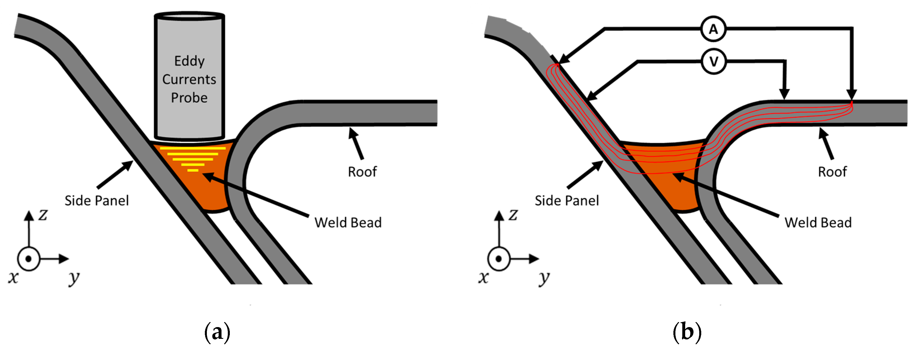
2. Materials and Methods
3. Results
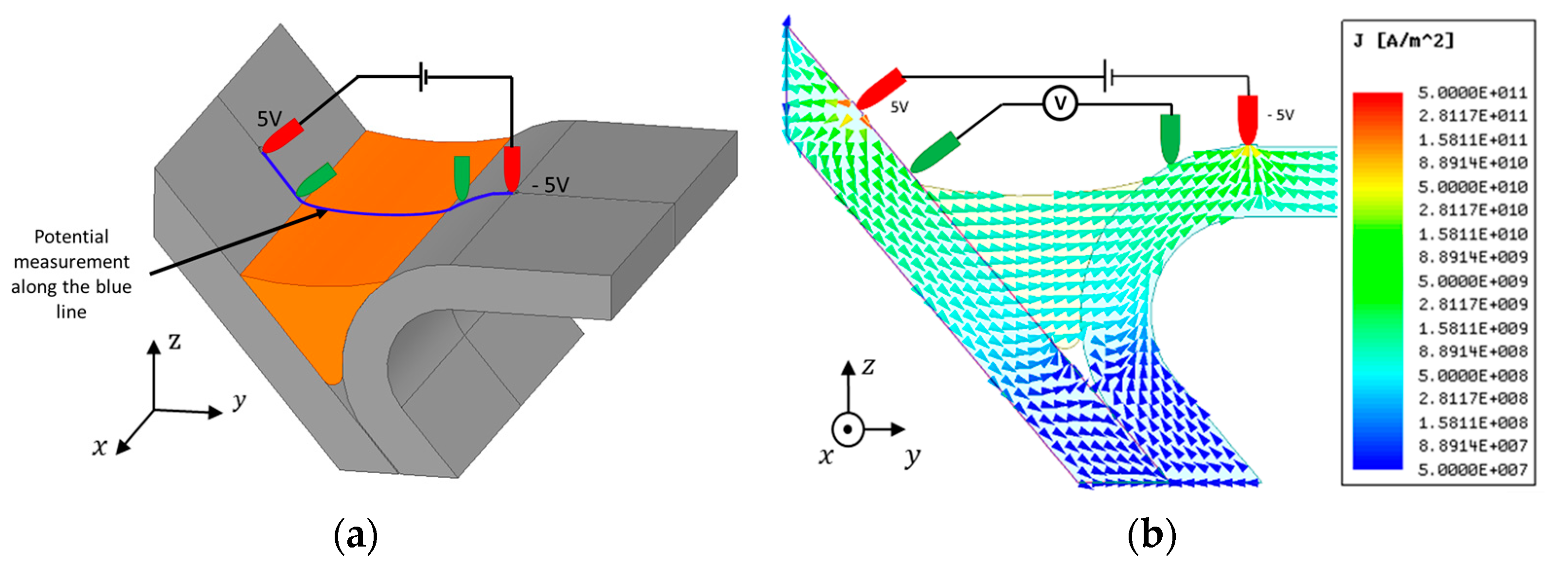
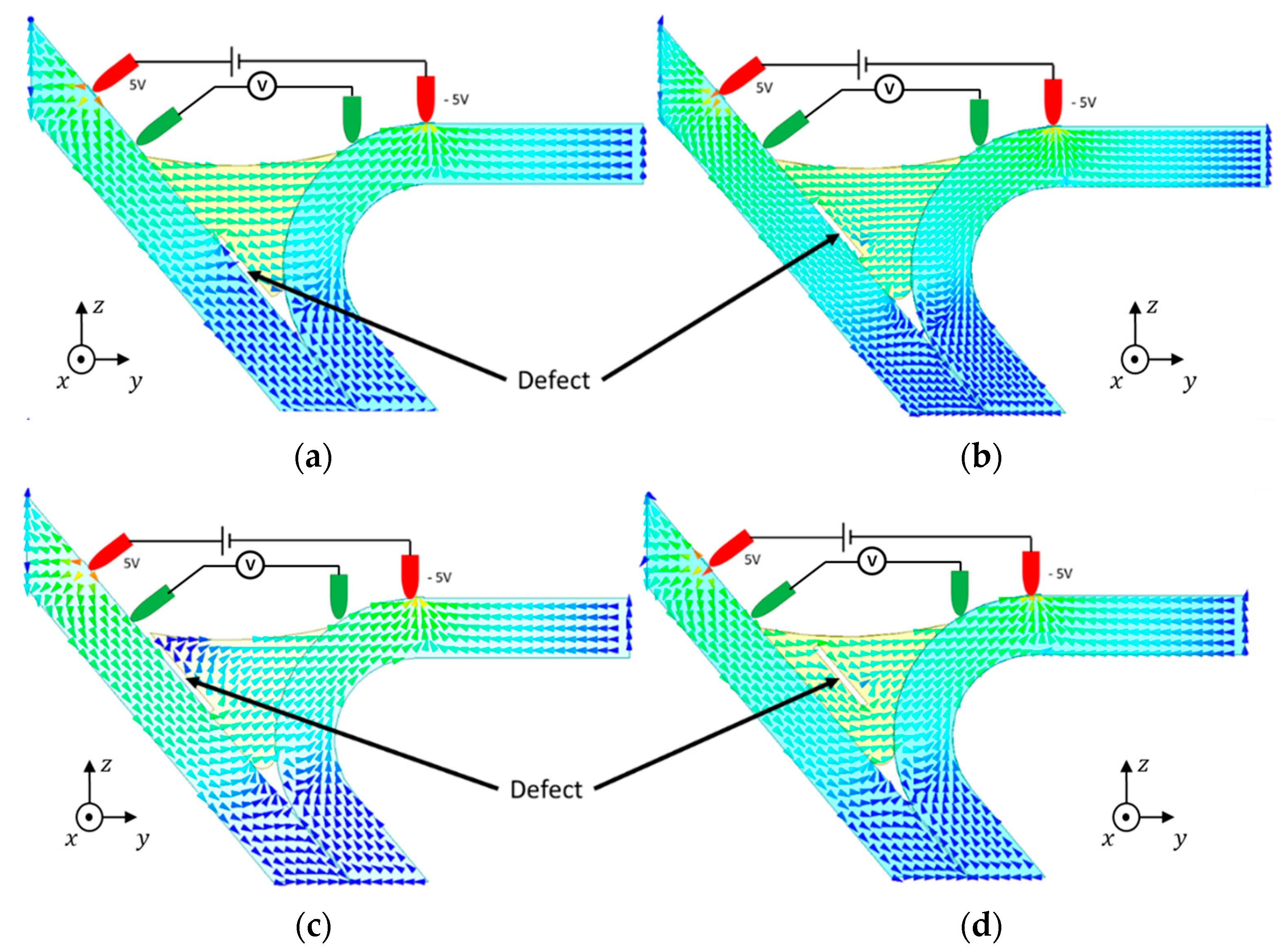
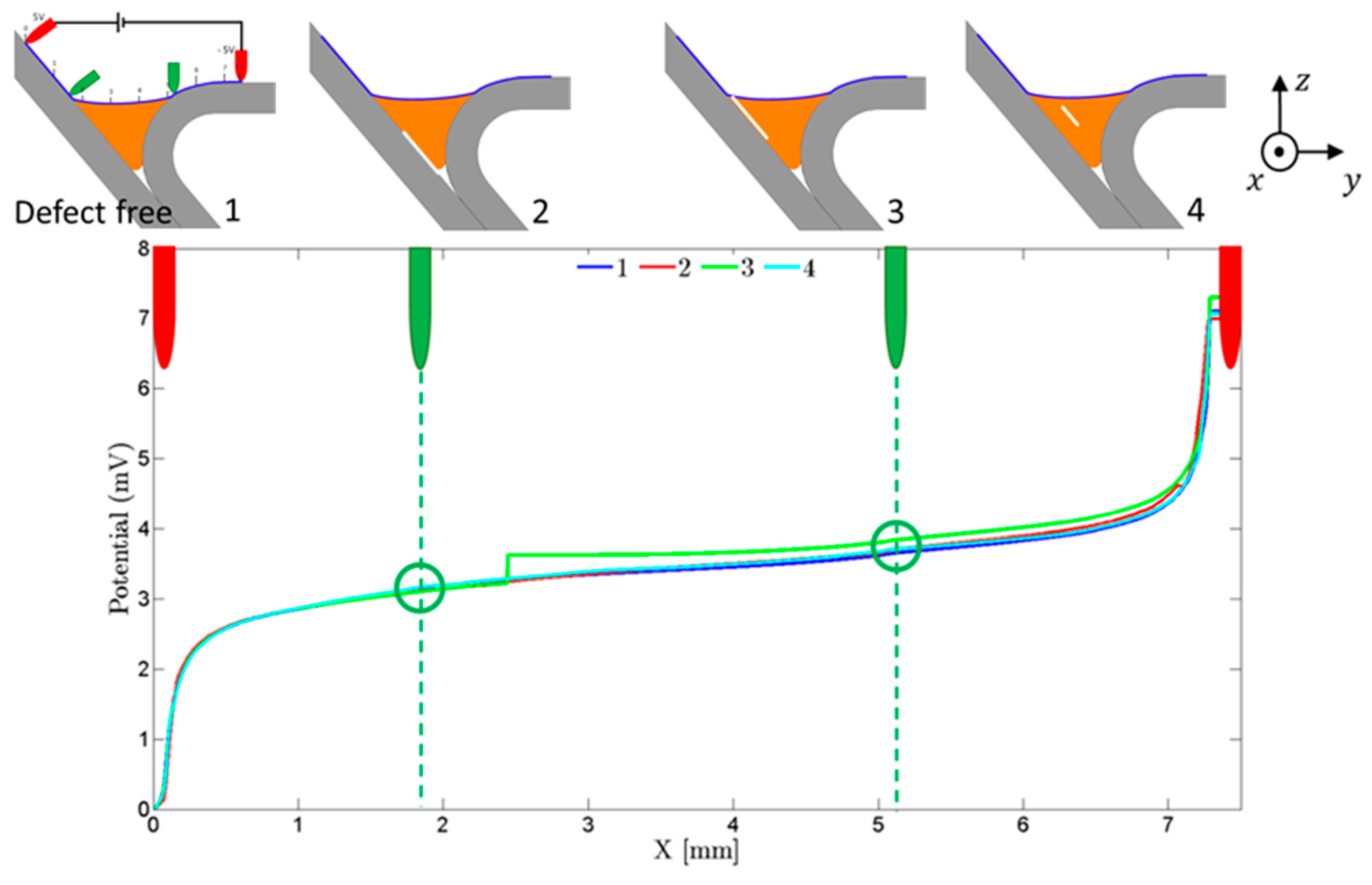
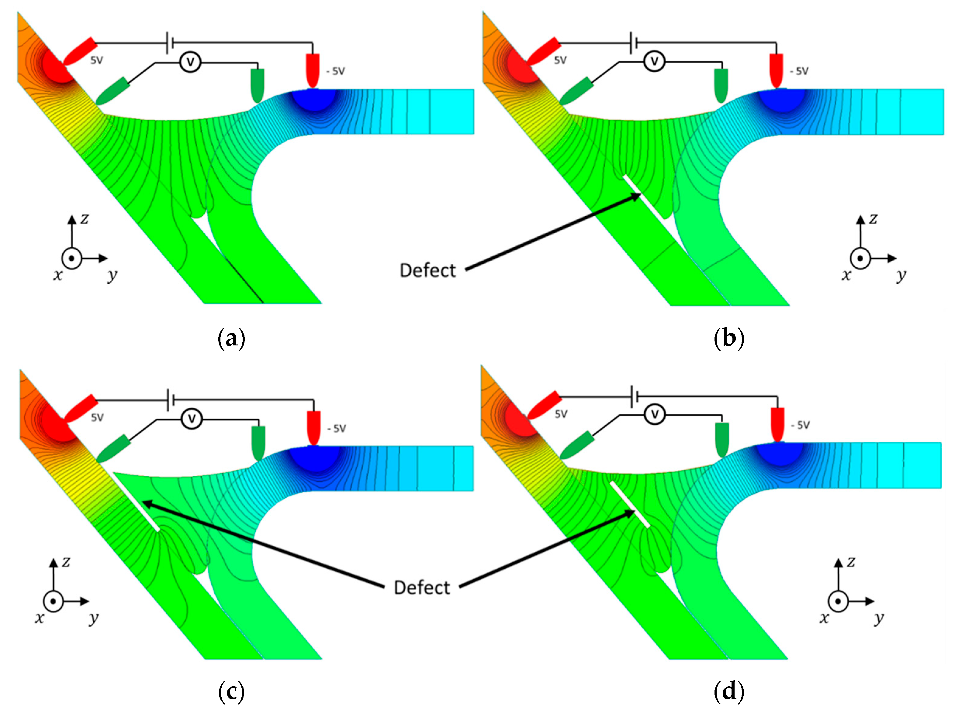
3.1. Numerical Simulation
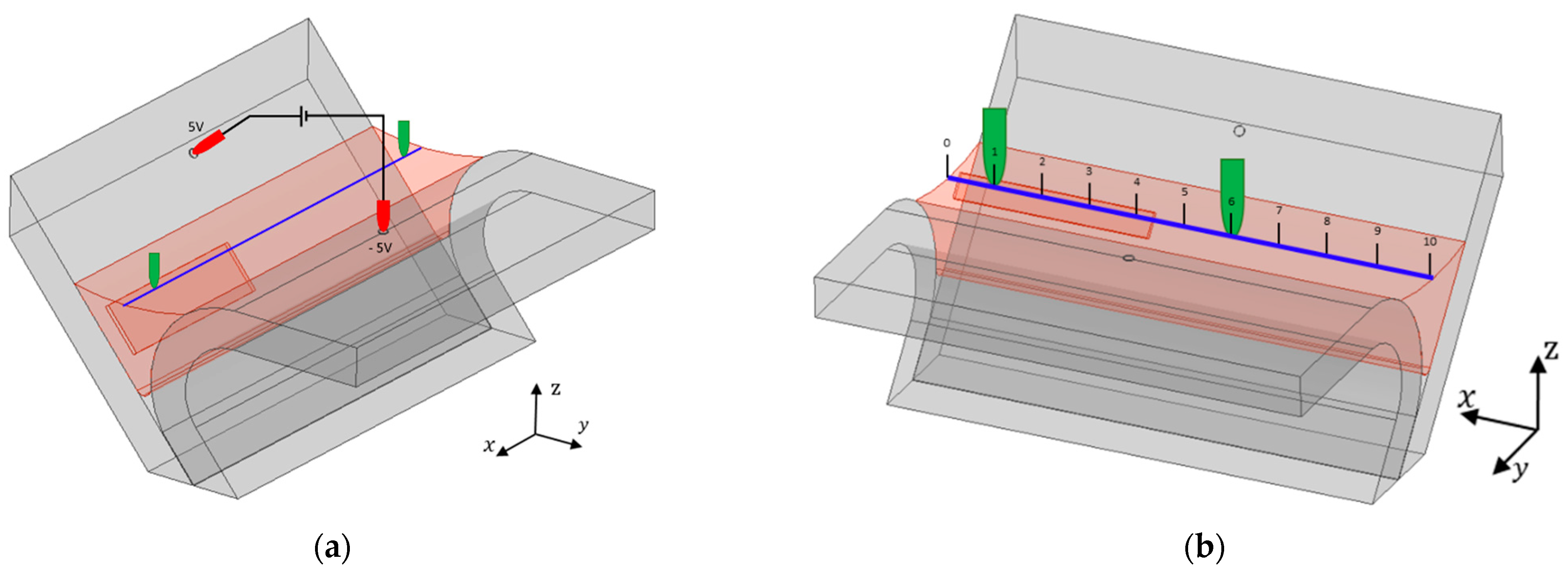
3.2. Four-Point Probe for Potential Drop Measurement
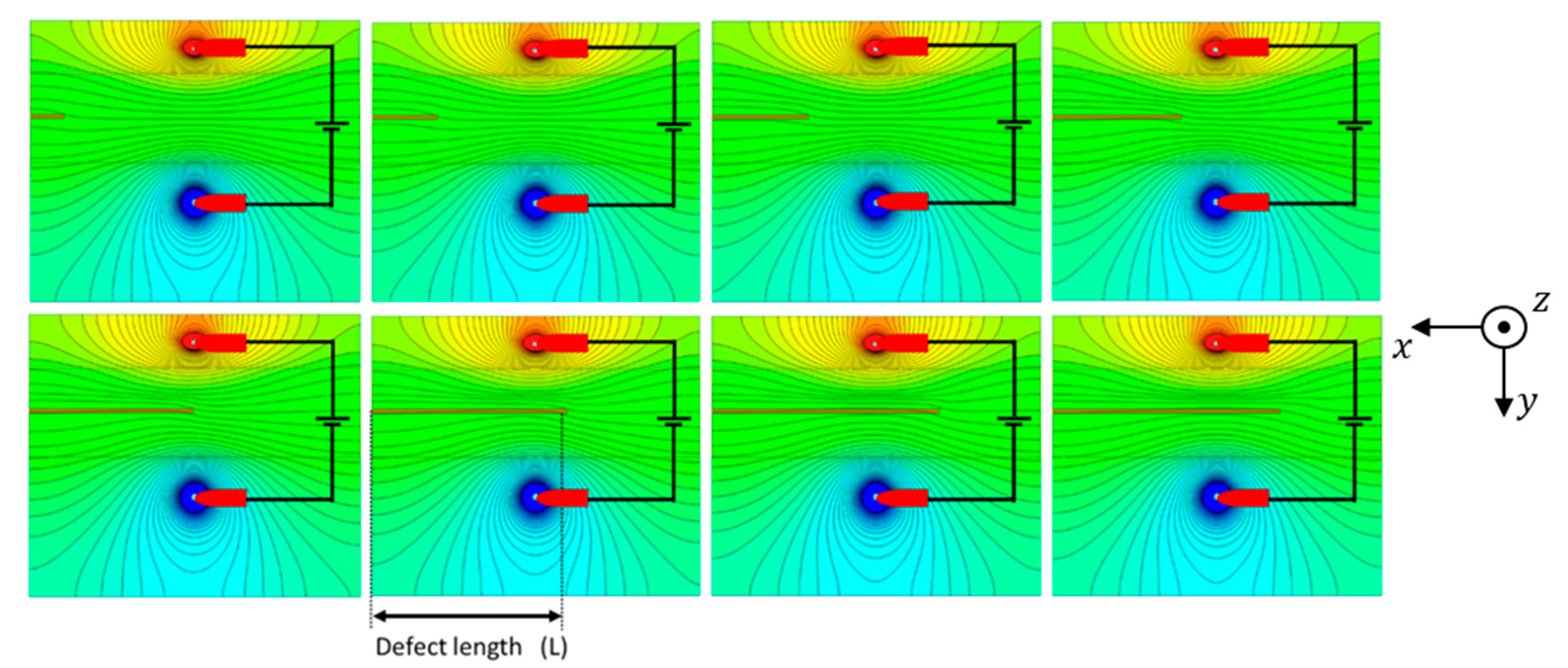
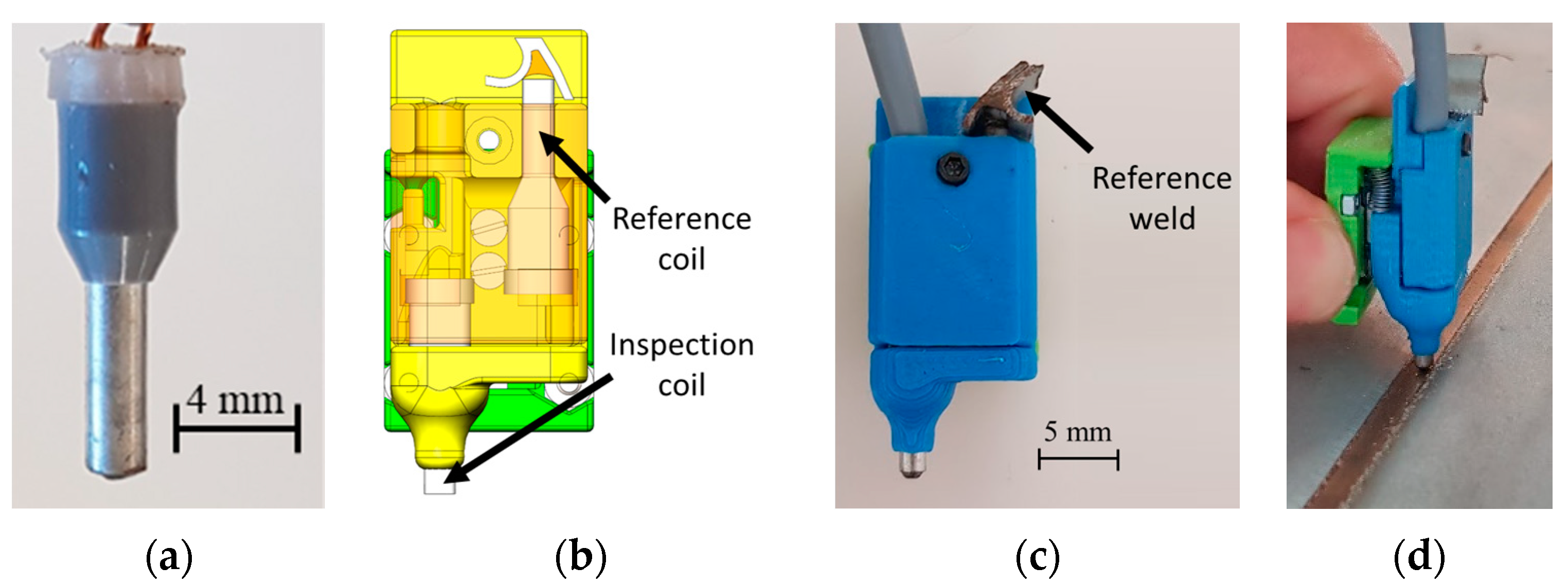
3.3. Eddy Current Probes
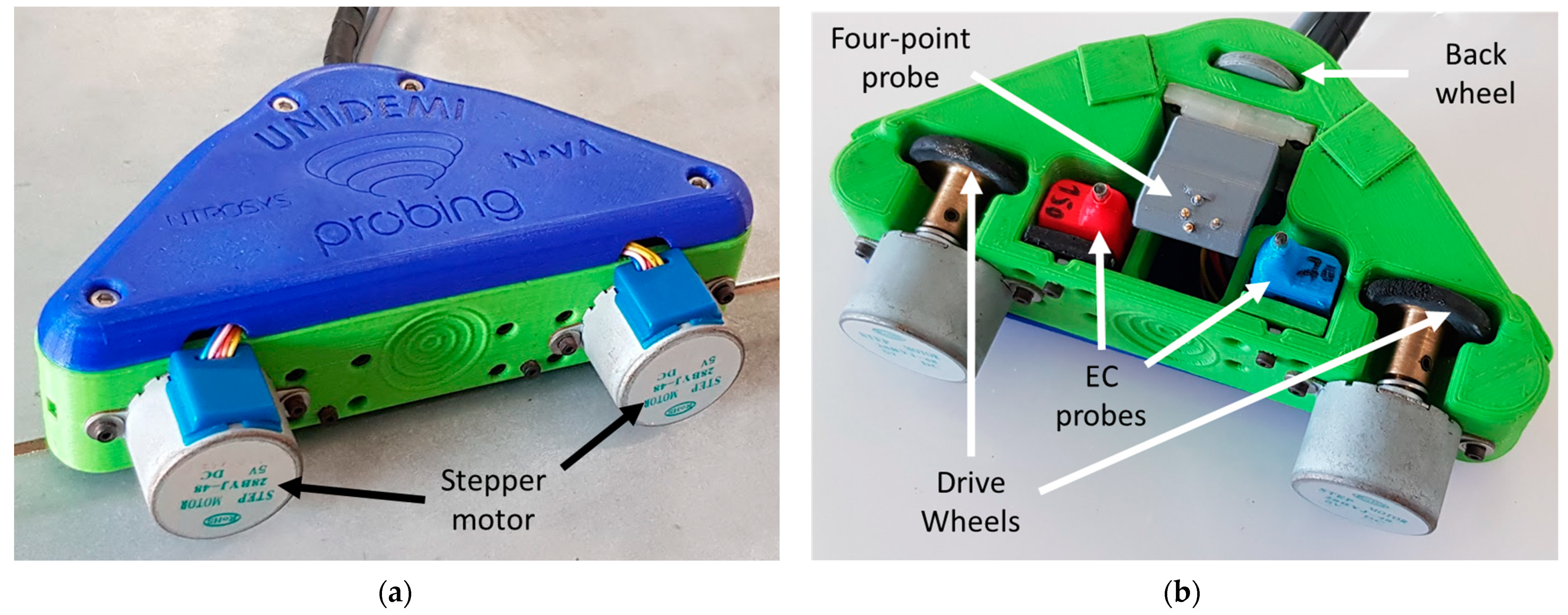
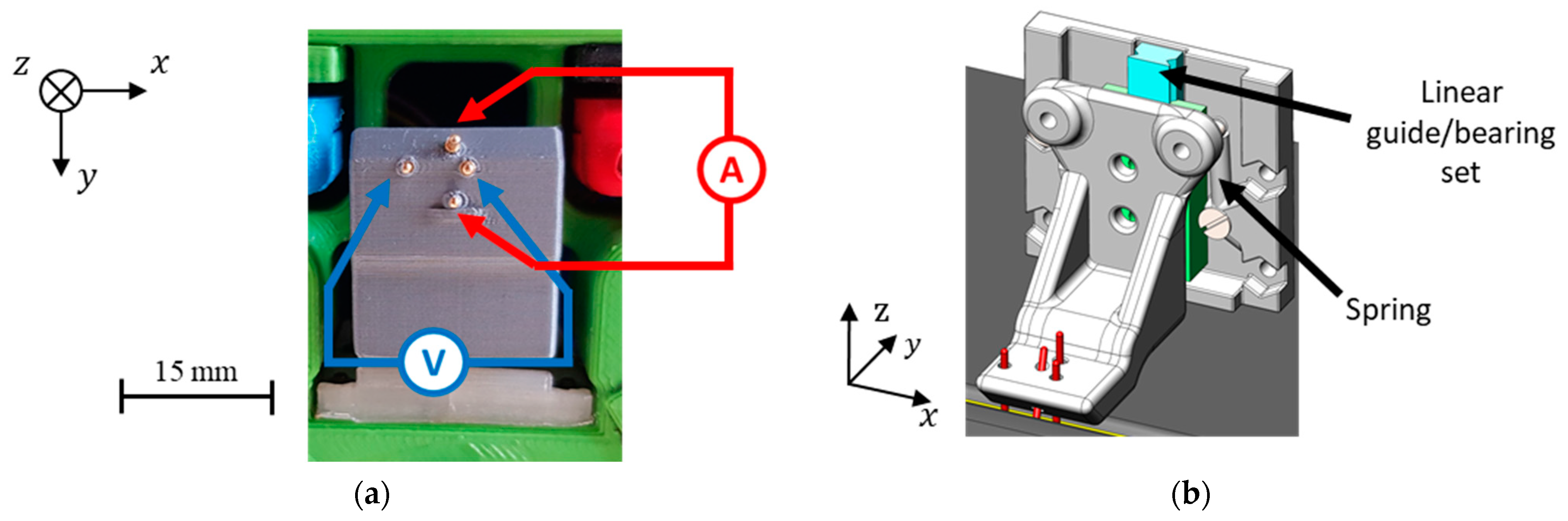
3.4. Scanning Device
3.5. Experimental Results
3.5.1. Sample Description
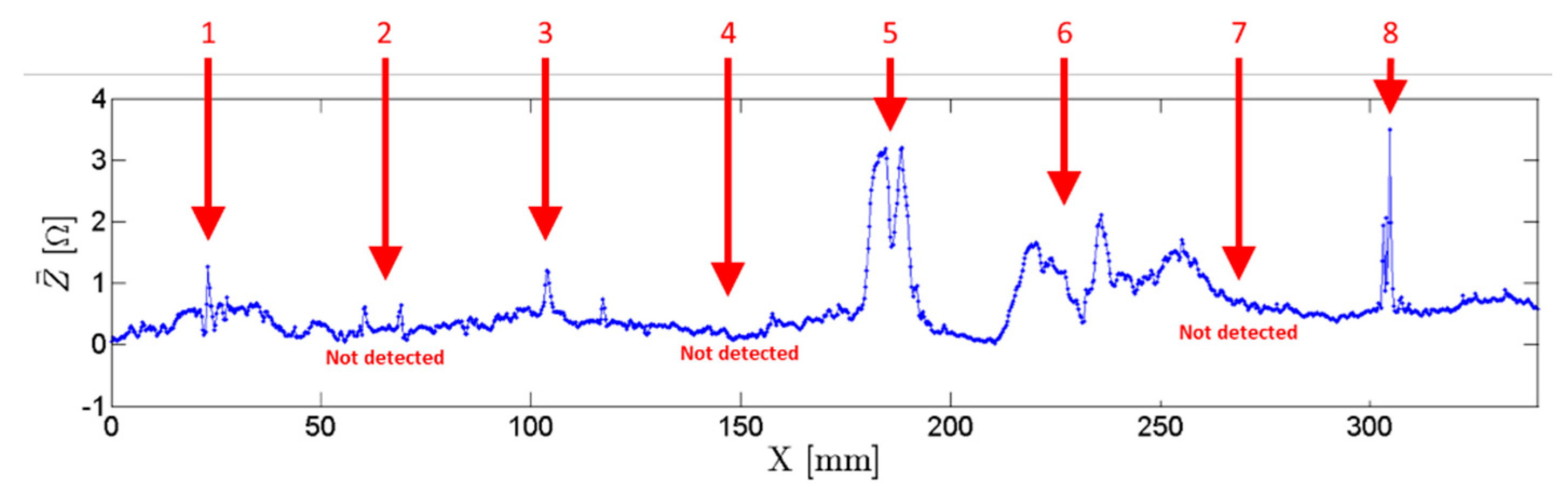
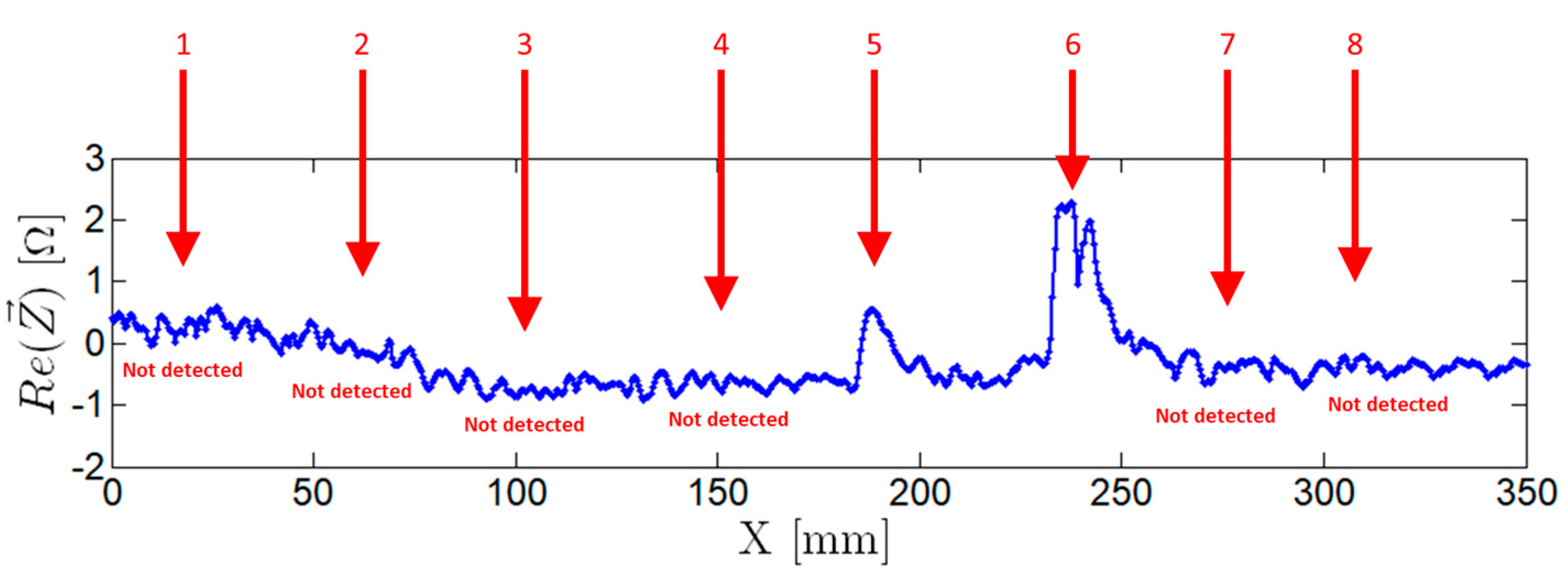
3.5.2. Eddy Currents and Analysis
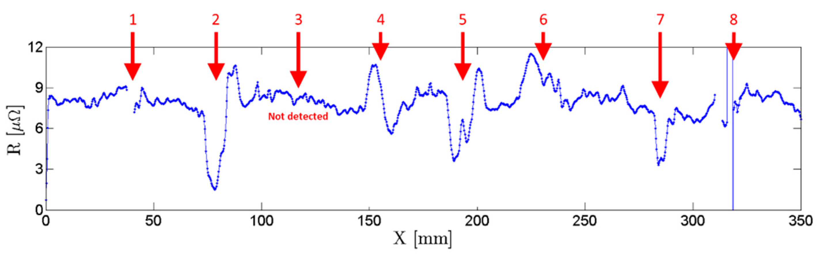
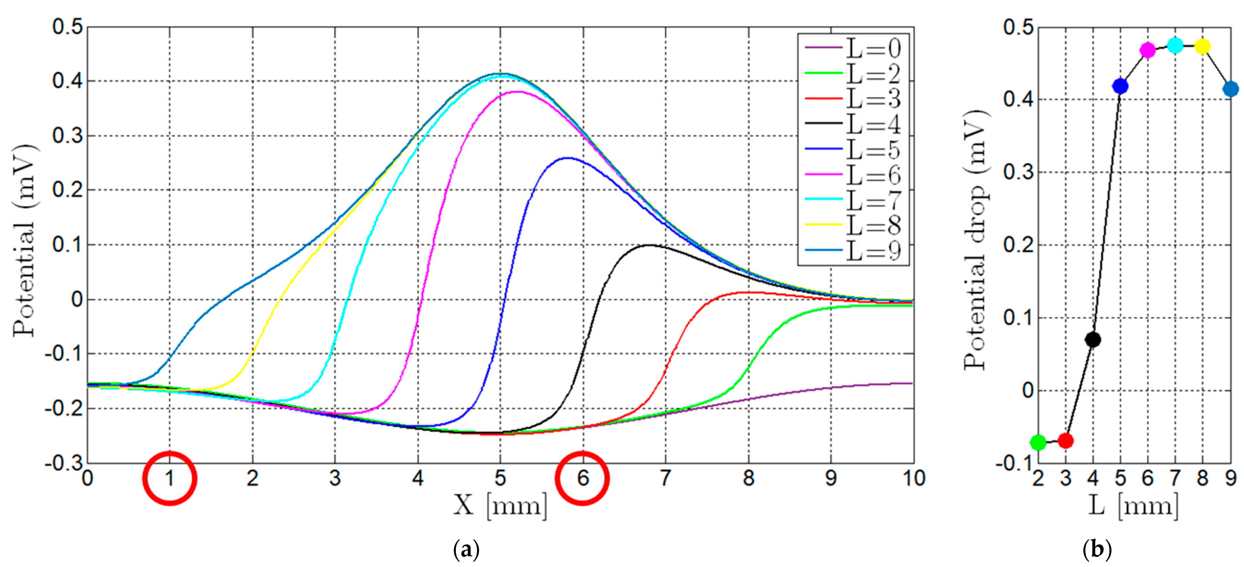
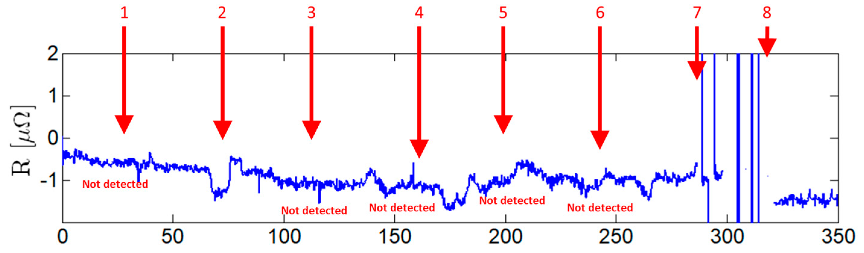
3.5.3. Potential Drop Measurement
4. Discussion and Conclusions
Author Contributions
Funding
Institutional Review Board Statement
Informed Consent Statement
Acknowledgments
Conflicts of Interest
References
- Krishnaja, D.; Cheepu, M.; Venkateswarlu, D. A Review of Research Progress on Dissimilar Laser Weld-Brazing of Automotive Applications. IOP Conf. Ser. Mater. Sci. Eng. 2018, 330, 012073. [Google Scholar] [CrossRef]
- Frank, S.; Ungers, M.; Rolser, R. Coaxial Control of Aluminum and Steel Laser Brazing Processes. Phys. Procedia 2011, 12, 752–760. [Google Scholar] [CrossRef]
- Stavridis, J.; Papacharalampopoulos, A.; Stavropoulos, P. Quality assessment in laser welding: A critical review. Int. J. Adv. Manuf. Technol. 2018, 94, 1825–1847. [Google Scholar] [CrossRef]
- Huang, W.; Kovacevic, R. Development of a real-time laser-based machine vision system to monitor and control welding processes. Int. J. Adv. Manuf. Technol. 2012, 63, 235–248. [Google Scholar] [CrossRef]
- Senthil Kumar, G.; Natarajan, U.; Ananthan, S.S. Vision inspection system for the identification and classification of defects in MIG welding joints. Int. J. Adv. Manuf. Technol. 2012, 61, 923–933. [Google Scholar] [CrossRef] [Green Version]
- Wang, W.; Cai, Y.; Wang, H.-P.; Carlson, B.E.; Poss, M. Quality inspection scheme for automotive laser braze joints. Int. J. Adv. Manuf. Technol. 2020, 106, 1553–1566. [Google Scholar] [CrossRef]
- Sato, Y.; Kim, H. Detection and sizing of cracks using potential drop techniques based on electromagnetic induction. E-J. Adv. Maint. 2011, 3, 39–53. [Google Scholar]
- Ösch, A.Z.; Eidel, M.S. Non Destructive Testing of Laser Welded Lap Seams by Eddy Current Technique. Evaluation 2006, 1–8. [Google Scholar]
- Todorov, E.; Nagy, B.; Levesque, S.; Ames, N.; Na, J. Inspection of laser welds with array eddy current technique. AIP Conf. 2013, 1511, 1065–1072. [Google Scholar] [CrossRef] [Green Version]
- Machado, M.A.; Rosado, L.F.S.G.; Mendes, N.A.M.; Miranda, R.M.M.; dos Santos, T.J.G. New directions for inline inspection of automobile laser welds using non-destructive testing. Int. J. Adv. Manuf. Technol. 2021, 1–13. [Google Scholar] [CrossRef]
- Nagy, P.B. NDT Techniques: Electrical. Ref. Modul. Mater. Sci. Mater. Eng. 2016. [Google Scholar] [CrossRef]
- Bär, J. Crack Detection and Crack Length Measurement with the DC Potential Drop Method–Possibilities, Challenges and New Developments. Appl. Sci. 2020, 10, 8559. [Google Scholar] [CrossRef]
- Raja, M.K.; Mahadevan, S.; Rao, B.P.C.; Behera, S.P.; Jayakumar, T.; Raj, B. Influence of crack length on crack depth measurement by an alternating current potential drop technique. Meas. Sci. Technol. 2010, 21, 105702. [Google Scholar] [CrossRef]
- Liu, X.; Qin, J.; Chen, Z.; Tian, S. Qualitative Study on Cable Breakage of Nb3Sn CICC Based on Direct Current Potential Drop Method. IEEE Trans. Appl. Supercond. 2021, 31, 1–4. [Google Scholar] [CrossRef]
- Riba, J.-R.; Gómez-Pau, Á.; Martínez, J.; Moreno-Eguilaz, M. On-Line Remaining Useful Life Estimation of Power Connectors Focused on Predictive Maintenance. Sensors 2021, 21, 3739. [Google Scholar] [CrossRef] [PubMed]
- Mahammed, M.S.; Faris, S.T. Cracks length OF AA7075 measurement under electrical potential drop technique. J. Mech. Eng. Res. Dev. 2021, 44, 158–169. [Google Scholar]
- Van Minnebruggen, K.; Hertelé, S.; Verstraete, M.A.; De Waele, W. Crack growth characterization in single-edge notched tension testing by means of direct current potential drop measurement. Int. J. Press. Vessel. Pip. 2017, 156, 68–78. [Google Scholar] [CrossRef]
- Xue, H.; Xu, P.; Ni, C.; Wei, Q.; Cui, Y.; Zhang, L.; Bashir, R. A Monitoring System for Crack Growth Rate Based on Direct Current Potential Drop. In Proceedings of the 2018 International Conference on Sensor Networks and Signal Processing, Xi’an, China, 28–31 October 2018; IEEE: Xi’an, China, 2018; pp. 317–321. [Google Scholar] [CrossRef]
- Campagnolo, A.; Bär, J.; Meneghetti, G. Analysis of crack geometry and location in notched bars by means of a three-probe potential drop technique. Int. J. Fatigue 2019, 124, 167–187. [Google Scholar] [CrossRef]
- Ryu, K.; Lee, T.; Baek, D.; Park, J. Pipe thinning model development for direct current potential drop data with machine learning approach. Nucl. Eng. Technol. 2020, 52, 784–790. [Google Scholar] [CrossRef]
- Tohmyoh, H.; Ikarashi, H.; Matsui, Y.; Hasegawa, Y.; Obara, S. Evaluation of the nugget diameter in spot welded joints between two steel sheets by means of a potential drop technique. Meas. Sci. Technol. 2015, 26, 085602. [Google Scholar] [CrossRef]
- Sorger, G.L.; Oliveira, J.P.; Inácio, P.L.; Enzinger, N.; Vilaça, P.; Miranda, R.M.; Santos, T.G. Non-destructive microstructural analysis by electrical conductivity: Comparison with hardness measurements in different materials. J. Mater. Sci. Technol. 2019, 35, 360–368. [Google Scholar] [CrossRef]
- Corcoran, J.; Nagy, P.B. Magnetic Stress Monitoring Using a Directional Potential Drop Technique. J. Nondestruct. Eval. 2018, 37, 60. [Google Scholar] [CrossRef] [PubMed] [Green Version]
- García-Martín, J.; Gómez-Gil, J.; Vázquez-Sánchez, E. Non-destructive techniques based on eddy current testing. Sensors 2011, 11, 2525–2565. [Google Scholar] [CrossRef] [PubMed] [Green Version]
- Huang, L.; Liao, C.; Song, X.; Chen, T.; Zhang, X.; Deng, Z. Research on Detection Mechanism of Weld Defects of Carbon Steel Plate Based on Orthogonal Axial Eddy Current Probe. Sensors 2020, 20, 5515. [Google Scholar] [CrossRef]
- Duarte, V.R.; Rodrigues, T.A.; MacHado, M.A.; Pragana, J.P.M.; Pombinha, P.; Coutinho, L.; Silva, C.M.A.; Miranda, R.M.; Goodwin, C.; Huber, D.E.; et al. Benchmarking of Nondestructive Testing for Additive Manufacturing. 3D Print. Addit. Manuf. 2021, 8, 263–270. [Google Scholar] [CrossRef]
- Santos, T.G.; Oliveira, J.P.; Machado, M.A.; Inácio, P.L.; Duarte, V.R.; Rodrigues, T.A.; Santos, R.A.; Simão, C.; Carvalho, M.; Martins, A.; et al. Reliability and NDT Methods. Addit. Manuf. Hybrid Process. Compos. Syst. 2020, 129, 265–295. [Google Scholar] [CrossRef]
- Machado, M.A.; Antin, K.-N.; Rosado, L.S.; Vilaça, P.; Santos, T.G. High-speed inspection of delamination defects in unidirectional CFRP by non-contact eddy current testing. Compos. Part B Eng. 2021, 224, 109167. [Google Scholar] [CrossRef]
- Antin, K.-N.; Machado, M.A.; Santos, T.G.; Vilaça, P. Evaluation of Different Non-destructive Testing Methods to Detect Imperfections in Unidirectional Carbon Fiber Composite Ropes. J. Nondestruct. Eval. 2019, 38, 23. [Google Scholar] [CrossRef] [Green Version]
- Fan, S.; Yi, J.; Sun, H.; Yun, F. Quantifying Hole-Edge Crack of Bolt Joints by Using an Embedding Triangle Eddy Current Sensing Film. Sensors 2021, 21, 2567. [Google Scholar] [CrossRef] [PubMed]
- Machado, M.A.; Rosado, L.; Pedrosa, N.; Miranda, R.M.; Piedade, M.; Santos, T.G. Customized Eddy Current Probes for Pipe Inspection. Stud. Appl. Electromagn. Mech. 2017, 42, 283–290. [Google Scholar] [CrossRef]
- Meng, X.; Lu, M.; Yin, W.; Bennecer, A.; Kirk, K.J. Evaluation of Coating Thickness Using Lift-Off Insensitivity of Eddy Current Sensor. Sensors 2021, 21, 419. [Google Scholar] [CrossRef] [PubMed]
- Rodrigues, N.M.; Rosado, L.S.; Ramos, P.M. A portable embedded contactless system for the measurement of metallic material conductivity and lift-off. Measurement 2017, 111, 441–450. [Google Scholar] [CrossRef]
- Bowler, N. Theory of four-point alternating current potential drop measurements on a metal half-space. J. Phys. D Appl. Phys. 2006, 39, 584–589. [Google Scholar] [CrossRef] [Green Version]
- Hua, S.; Li, B.; Shu, L.; Jiang, P.; Cheng, S. Defect detection method using laser vision with model-based segmentation for laser brazing welds on car body surface. Measurement 2021, 178, 109370. [Google Scholar] [CrossRef]
- Cheng, L.; Mi, G.; Li, S.; Wang, C.; Hu, X. Defects diagnosis in laser brazing using near-infrared signals based on empirical mode decomposition. Opt. Laser Technol. 2018, 100, 12–20. [Google Scholar] [CrossRef]


| N° | Picture | N° | Picture |
|---|---|---|---|
| 1 | Surface welded defect | 5 | Interface defect between steel and weld |
| 2 | Surface welded defect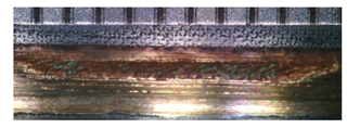 | 6 | Interface defect between steel and weld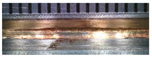 |
| 3 | Interface defect between steel and weld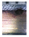 | 7 | Interface defect between steel and weld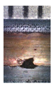 |
| 4 | Interface defect between steel and weld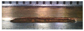 | 8 | Surface welded defect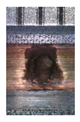 |
Test piece | |||
Publisher’s Note: MDPI stays neutral with regard to jurisdictional claims in published maps and institutional affiliations. |
© 2021 by the authors. Licensee MDPI, Basel, Switzerland. This article is an open access article distributed under the terms and conditions of the Creative Commons Attribution (CC BY) license (https://creativecommons.org/licenses/by/4.0/).
Share and Cite
Machado, M.A.; Rosado, L.S.; Mendes, N.M.; Miranda, R.M.; Santos, T.G. Multisensor Inspection of Laser-Brazed Joints in the Automotive Industry. Sensors 2021, 21, 7335. https://doi.org/10.3390/s21217335
Machado MA, Rosado LS, Mendes NM, Miranda RM, Santos TG. Multisensor Inspection of Laser-Brazed Joints in the Automotive Industry. Sensors. 2021; 21(21):7335. https://doi.org/10.3390/s21217335
Chicago/Turabian StyleMachado, Miguel A., Luís S. Rosado, Nuno M. Mendes, Rosa M. Miranda, and Telmo G. Santos. 2021. "Multisensor Inspection of Laser-Brazed Joints in the Automotive Industry" Sensors 21, no. 21: 7335. https://doi.org/10.3390/s21217335
APA StyleMachado, M. A., Rosado, L. S., Mendes, N. M., Miranda, R. M., & Santos, T. G. (2021). Multisensor Inspection of Laser-Brazed Joints in the Automotive Industry. Sensors, 21(21), 7335. https://doi.org/10.3390/s21217335