You are currently viewing a new version of our website. To view the old version click .
Sensors
  • Article
  • Open Access

27 October 2021

A Manycore Vision Processor for Real-Time Smart Cameras †

,
,
,
and
1
Automation & Control Group, University of Brasilia, Brasilia 70910-900, Brazil
2
Graduate Program in Electrical Engineering, Department of Electronic Engineering, Federal University of Minas Gerais (UFMG), Belo Horizonte 31270-901, Brazil
3
Computer Engineering, Technical University Brandenburg, 03046 Brandenburg, Germany
*
Author to whom correspondence should be addressed.
This article belongs to the Special Issue Camera as a Smart-Sensor (CaaSS)

Abstract

Real-time image processing and computer vision systems are now in the mainstream of technologies enabling applications for cyber-physical systems, Internet of Things, augmented reality, and Industry 4.0. These applications bring the need for Smart Cameras for local real-time processing of images and videos. However, the massive amount of data to be processed within short deadlines cannot be handled by most commercial cameras. In this work, we show the design and implementation of a manycore vision processor architecture to be used in Smart Cameras. With massive parallelism exploration and application-specific characteristics, our architecture is composed of distributed processing elements and memories connected through a Network-on-Chip. The architecture was implemented as an FPGA overlay, focusing on optimized hardware utilization. The parameterized architecture was characterized by its hardware occupation, maximum operating frequency, and processing frame rate. Different configurations ranging from one to eighty-one processing elements were implemented and compared to several works from the literature. Using a System-on-Chip composed of an FPGA integrated into a general-purpose processor, we showcase the flexibility and efficiency of the hardware/software architecture. The results show that the proposed architecture successfully allies programmability and performance, being a suitable alternative for future Smart Cameras.

1. Introduction

The emergence of new trends in technology, such as the Internet of Things and Industry 4.0, pulled out several applications based on image processing and computer vision (IP/CV) techniques. Cyber-physical systems, augmented reality, and autonomous machines, among others, all have applications supported by the extensive use of cameras. Most of the conventional cameras are designed for the acquisition and transmission of images and videos. These cameras are not able to support complete applications running under real-time constraints. For these reasons, there is a need for devices capable of acquiring and processing images and videos efficiently and in real-time.
Images are inherently parallel, and the literature shows that for the IP/CV domain, the efficient parallelism exploration is the key for performance improvement. The underlying hardware/software architecture, as well as the programming model offered to the users, must be designed under application-specific constraints to reach higher performance [1,2,3]. To explore the parallelism massively, our approach was to parallelize the processing right after image capture by the pixel sensor. Figure 1 shows the concept used, in which the image is divided into parallel processing units [4].
Figure 1. The intrinsic IP/CV parallelism explored using multiple processing tiles.
Hardware architectures span a broad diversity: ASICs, direct field-programmable gate array (FPGA) implementations, application-specific instruction set processors (ASIPs), very-large instruction word (VLIW) processors, digital signal processors (DSPs), graphics processing units (GPUs), and multi-processor System-on-Chip (MPSoCs), etc. Each approach is an attempt to explore data parallelism, higher processing frequencies, pipelines, or complex instructions. Considering the characteristics of pixel parallelism, depicted in Figure 1, as well as in previous findings from the literature, we propose an IP/CV application-specific architecture: a manycore vision processor system. All hardware/software design decisions are based on IP/CV application-specific needs, from the processing elements microarchitecture to the Network-on-Chip (NoC) interconnects. A general-purpose processor (GPP) and a direct memory access (DMA) scheme complement the manycore to build a novel heterogeneous smart camera architecture.
The rest of this work is organized as follows: Section 2 depicts a literature review of the main challenges in the area, the state-of-art solutions, as well as the gaps we propose to cover with this work. In Section 3, we explain the HW/SW organization, the main design decisions, and implementation details of each hardware block. Section 4 explains the application used to characterize the HW/SW architecture. Section 5 presents and discusses the results. Finally, in Section 6, we present the conclusion and future works.

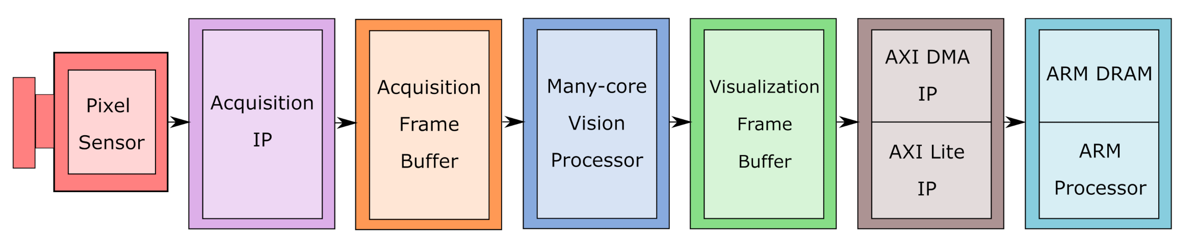
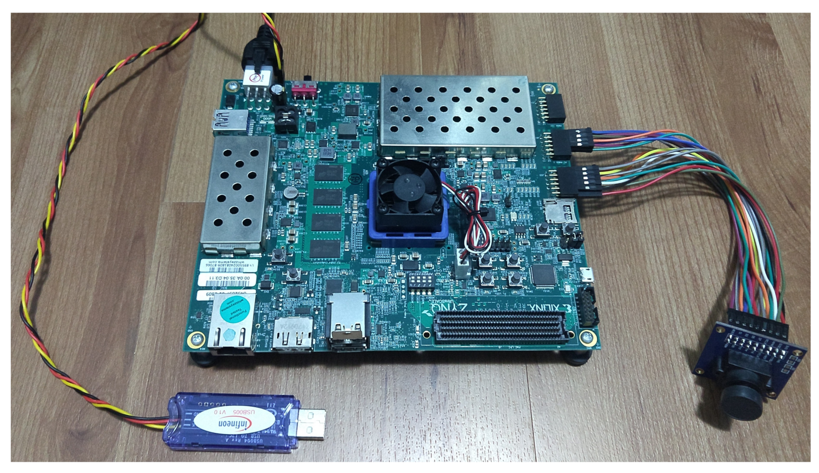
3. The HW/SW Platform

The architecture proposed in this work was designed considering the diversity and complexity of IP/CV algorithms, the parallelism exploration on different abstraction levels, and the hardware costs. Figure 2 shows the block diagram of the complete Smart Camera proposed [21]. We selected a ZYNQ Ultrascale+ device (ZCU104 development kit from Xilinx), a state-of-art SoC [22], which integrates a GPP with an FPGA fabric in the same chip. The first block is a common pixel sensor module, which connects to the development board through a GPIO port. The ZYNQ Chip receives the pixel stream and stores the input image in the acquisition frame buffer. The pixels are then distributed among the tiles within the manycore vision processor to be processed. After the image processing, the output image is stored in the visualization frame buffer, which is then read out through DMA by an ARM processor, integrated into the SoC. The next sections explain in detail all the Smart Camera components.
Figure 2. Block diagram of the complete Smart Camera system.

3.1. Pixel Sensor

This work uses the OmniVision OV7670 CMOS sensor [23], a commercial OEM model with industry standard parallel interface. The sensor is set to QVGA resolution, 320 × 240 pixels, achieving up to 60 frames per second in the current setting. It outputs pixels in RGB444 encoding, which is therefore converted to grayscale in the Acquisition IP. The sensor pins are connected directly to the ZCU104 board through two GPIO interfaces, as shown in Figure 3 [21].
Figure 3. Photography of the Xilinx ZCU104 development kit with the OV7670 CMOS sensor and the Infineon power monitor device.

3.2. Acquisition IP and Acquisition Frame Buffer

The Acquisition IP is a group of different modules: to control the CMOS sensor, to receive pixel data, and to store it in the acquisition frame buffer. This scheme uses an open-source project [24] as the main reference with modifications.
Five modules, i.e., AXI Camera Control IP, Debounce, OV7670 Capture, RGB444 to Grayscale and OV7670 Controller, compose the IP, either for control or data sampling. OV7670 Controller module is responsible for the CMOS initialization. The controller sets the image size, output data format (RGB444 in this case), prescaler, contrast, gamma, UV auto adjust, image orientation, color conversion, VSYNC/HREF setups, and other configurations.
The sensor could be configured to output YUV format, avoiding the use of RGB to grayscale conversion; however, we wanted to show that it is also possible to explore direct FPGA IP/CV implementations, such as the ones depicted in Section 2.

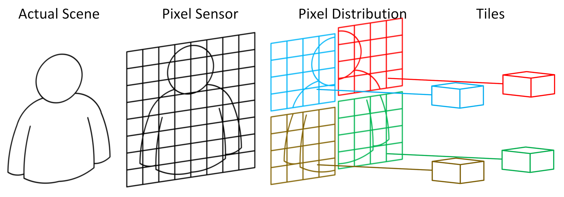
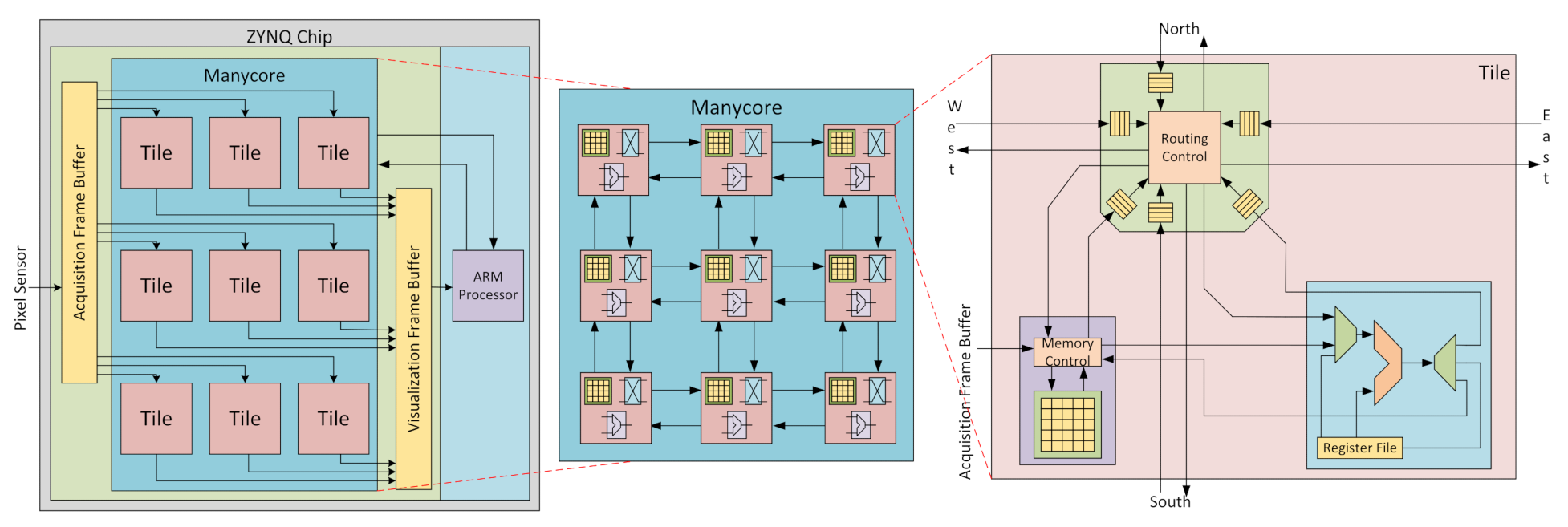
3.3. Manycore Vision Processor
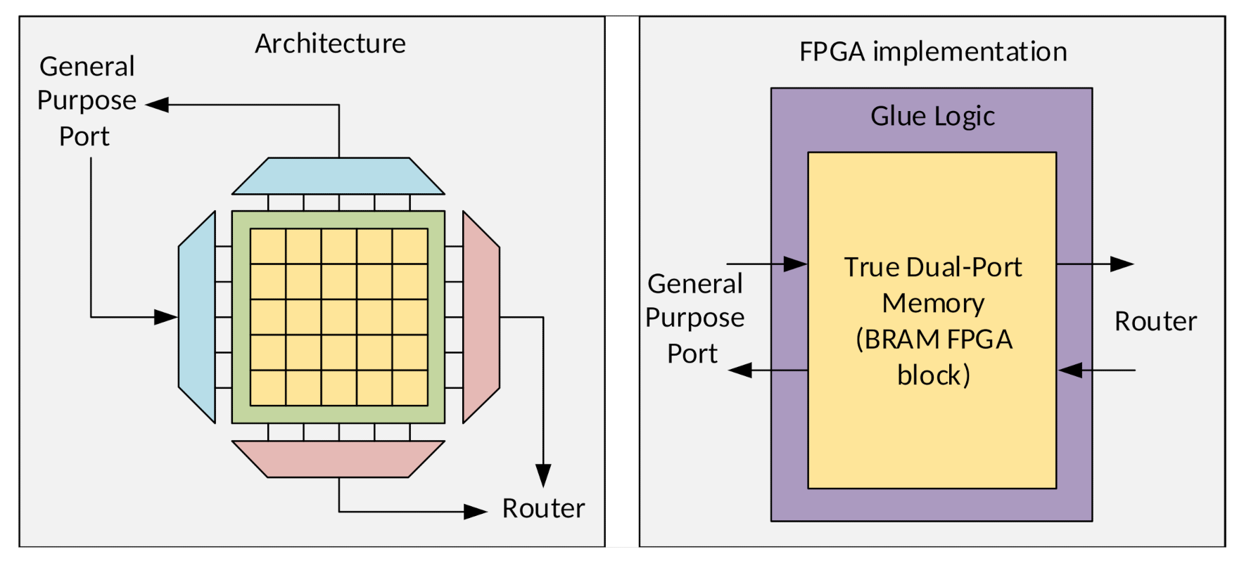
This section describes the manycore vision processor architecture and its HW/SW integration, as shown in Figure 4 [4]. It is made of basic units, called tiles, that process and store pixel values in memory and communicate with the other tiles using a router. Multiple tiles form a 2D-mesh Network-on-Chip, which transmits pixel data and control messages, forming a homogeneous manycore processing system. We run the same program code in all tiles to explore natural pixel parallelism, providing the usability at the IP/CV domain.
Figure 4. The manycore hardware architecture designed in our work.

3.3.1. Pixel Memory

The PM has to interface with the router, the PE, and also interact with external components such as the ARM processor or the input/output image buffers, as shown in Figure 5 [21]. Each pixel memory ideally stores a defined image region. In practice, there are some exceptions in border tiles, where it can have more storage than pixels in its sub-image. This happens because pixels can not be equally divided in regions depending on the manycore size. Furthermore, our automation tool has limitations and does not optimize the image slice for multiple architectures, which is not possible depending on the image resolution and MCVP size. However, for simplicity, these exceeding addresses are not taken into account in the implemented algorithms. Furthermore, Vivado’s block memory code generator cannot cut the exact BRAM slices depending on the architecture and image configurations due to its physical limitations, but it does not affect the implementations.
Figure 5. The pixel memory architecture.

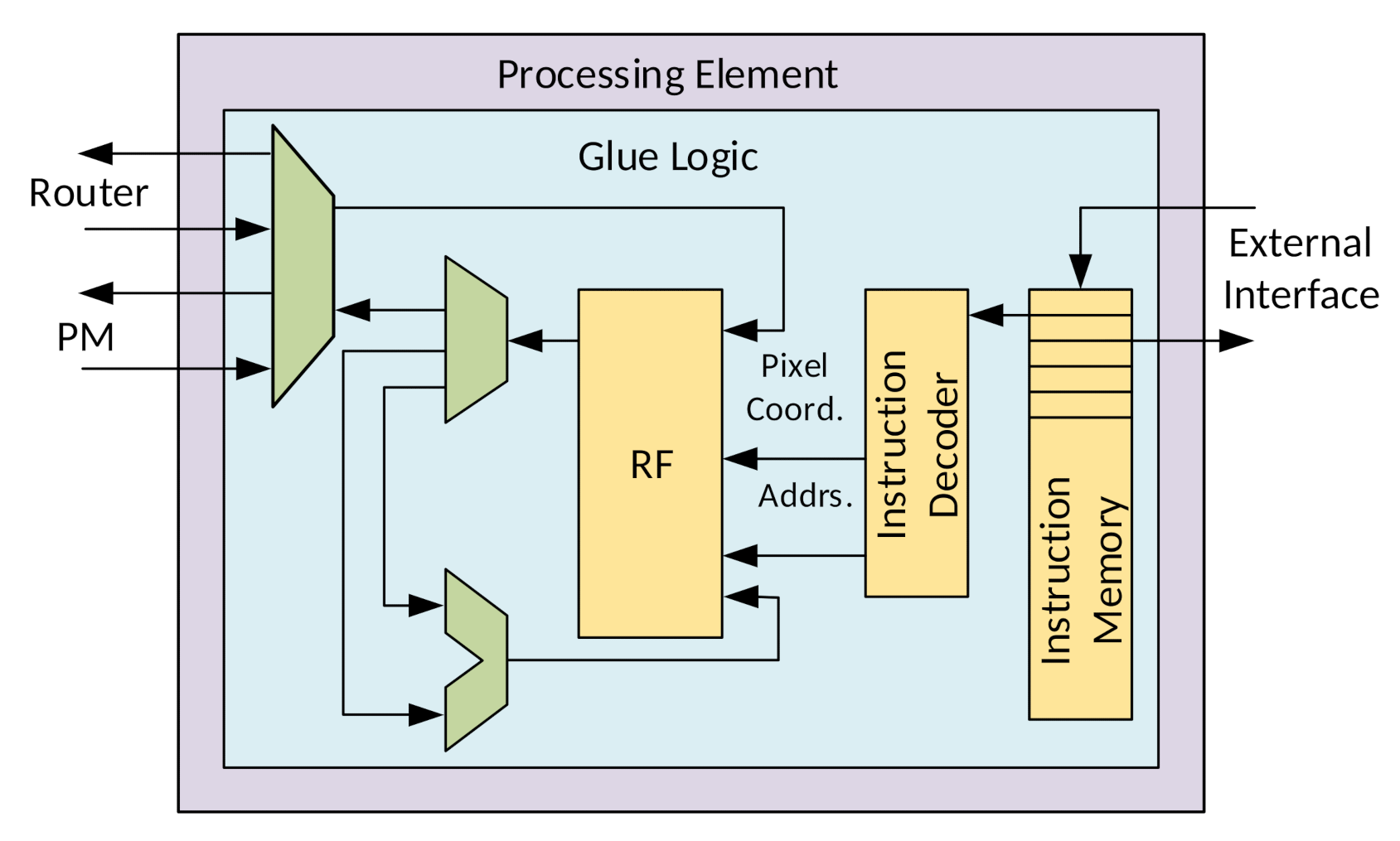
3.3.2. Processing Element
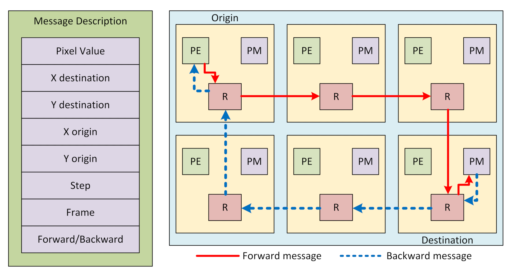
Processing elements must be able to perform simple computations such as basic arithmetic and branch operations. Furthermore, they must be compliant with the application-specific needs of IP/CV algorithms. With that in mind, a minimalist RISC processor, with only 16 instructions, was designed, as shown in Figure 6 [21]. The PEs have access to the register file and to the PM to use in tasks. Instruction memories store programming code for execution.
Figure 6. Processing element microarchitecture for P-type and R-type instructions.
The PE was developed focusing on: basic arithmetic operations necessary to most image processing algorithms, defined here as R-type instructions; branch and jump operations to control flow, named as Branch and Jump instructions, respectively; pixel data communication (P-type) and Control instructions. Those five constitute all instruction formats necessary for the PE to implement any type of IP/CV algorithm, turning the PE in a Turing-complete machine.

3.3.3. Router

The router is the component responsible for exchanging pixels among the tiles. Its interface consists of 6 ports, each one with one input and one output channel. All the channels are unidirectionally connected to the neighboring tiles (N, S, E, W) and the local PE and PM. Between each tile pair, there are message buffers used to avoid network stalls. The size of these buffers is configurable and depends on the algorithms used and the overall architecture configuration (image resolution and number of tiles). Figure 7 illustrates a message and how it is routed through the manycore [21].
Figure 7. Message description and route.
For example, if a PE has to perform a get-pixel instruction (GPX), which means that it needs a specific pixel at the RF to process, the PE wrapper verifies if the pixel belongs to its image region or another one. If it is a local pixel, the wrapper asks the local PM for the pixel value. In the case that a pixel is in another image region, the wrapper asks the local router. The router has an arbiter and, when it is the PE communication slot, the router decodes the destination and forwards the message to a neighbor router. Take Figure 7 as a sample, the top left tile requests a pixel that belongs to the bottom right one. Because of this distribution, the forward message passes through all routers in the red arrow route until it arrives at its destination. After obtaining the desired pixel, the PM sends it to the nearest router, which passes the message (as shown by the dashed blue arrow) to neighbor routers until the pixel arrives at its origin.

3.4. Visualization Frame Buffer

The visualization frame buffer controls pixel transfer from the manycore vision processor to the ARM processor, after the MCVP ends the processing of a frame. It has one AXI4-Lite interface to control and read relevant data from visualization FB. Furthermore, a memory interface, made of a true dual-port block RAM with two write ports in read-first mode [25], stores pixels written by the MCVP. This IP deals with two interfaces to link the manycore with the ARM processor: a memory interface from the MCVP, and an AXI4 Stream interface to communicate with the AXI DMA IP.
An AXI4 Stream interface sends data without ARM direct intervention. This approach reduces the processor load but demands a new IP to convert the stream to memory-mapped transfer (AXI DMA IP) and a finite state machine to read pixels from the block RAM and send it through AXI Stream interface.

3.5. AXI Direct Memory Access IP

This work uses an AXI direct memory access (DMA) IP [26] to write inside ARM’s DRAM. The work uses this model to deal with the DMA to reduce ARM’s workload. Another way to use it is to interrupt the processor every time a DMA iteration is complete. Them, the IP needs to be reprogrammed and so forth. Using descriptors, there is no need to interrupt the processor and reprogram anything, although it is still possible to interrupt the processor if necessary.
In the implemented design, one memory segment is reserved for the image, but the architecture can handle even multichannel cases. This situation can deal with two distinct cameras for stereo computer vision, for example.

3.6. ARM Processor

This work uses a Zynq UltraScale+ XCZU7EV-2FFVC1156 MPSoC with an ARM Cortex-A53-based application processing unit (APU) from the ZCU104 development kit. In this work, the ARM processor runs a bare-metal implementation, using only a single core from the four available. The ARM has PL-PS interruption enabled to address DMA IP needs. Furthermore, the initialization process and other low-level tools are all dealt with by Xilinx proprietary tools: the Vivado Design Suite to synthesize and implement the architecture, and the Xilinx Software Development Kit to handle software and FPGA setup.
The ARM processor is used to configure, program, monitor and debug the manycore system, as well as to contribute to the IP/CV application in higher abstraction levels. It communicates to the manycore system through the AXI (Lite/DMA) interfaces described earlier in the text. Through these interfaces, the ARM processor has access to pixel memories (PMs), instruction memories (IMs), and special-purpose registers for control and debug purposes.

4. Application Domain Analysis

The architecture proposed in this work aims to implement any type of IP/CV applications. In this context, we decided to show its flexibility with the implementation of an application suitable to explore different types of IP/CV algorithms: a motion estimation using the Harris corner detector (HCD). Several IP/CV algorithms manipulate pixels in similar ways. The Khronos group consortium established the OpenVX standard as a set of IP/CV functions selected as the most representative components of more complex applications.
In Table 2, we classify all 58 OpenVX functions into five classes, depending on how the image pixels are analyzed/manipulated [27]. In the first class, there are some complex applications, which can be built by combining functions from other classes. The last three classes are the lower-level ones and responsible for direct pixel manipulation. These classes are the most computationally expensive, and efficiently explored by our architecture. To show the performance of our solution for the IP/CV application domain, we selected an application from the first class, which we consider as representative of the most common applications in this domain: a motion estimation based on the Harris corner detector.
Table 2. Classification of the 58 OpenVX functions by operation structure.

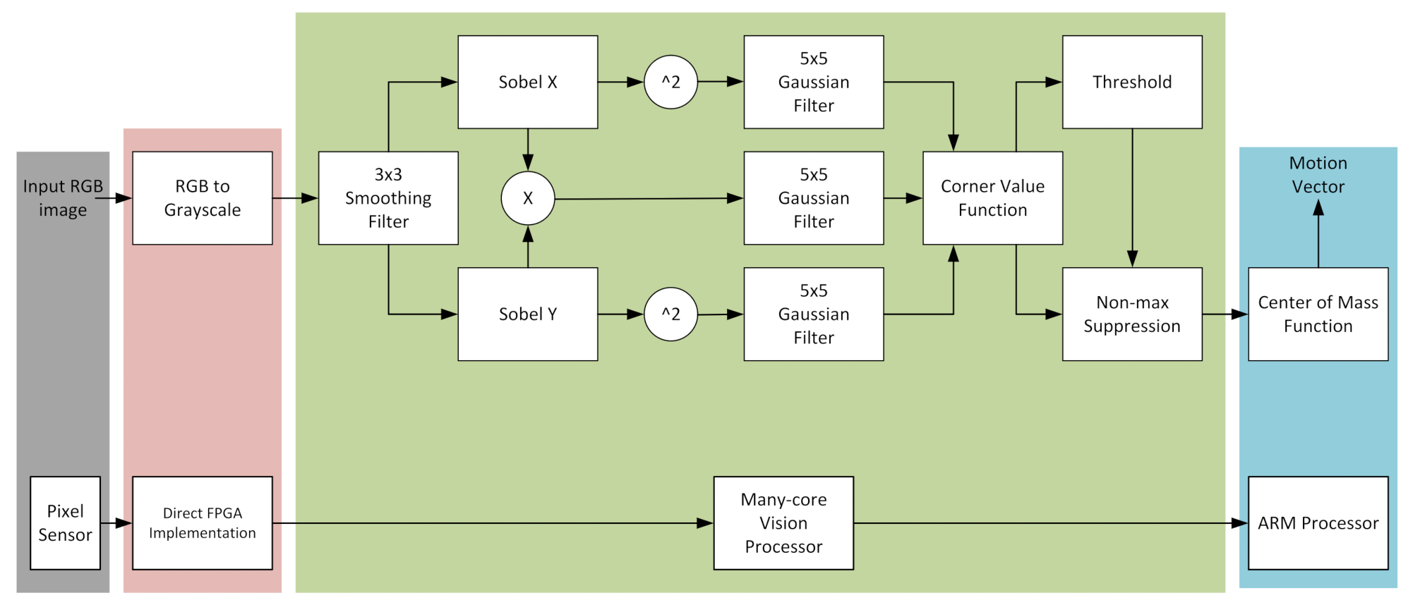
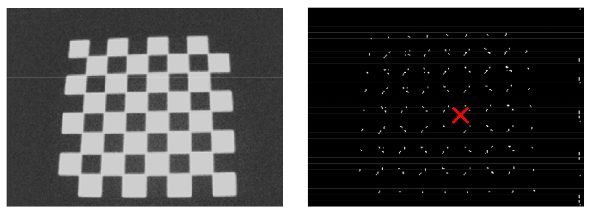
4.1. Harris Corner Detector

Figure 8 shows the HCD processing chain based on common textbook implementations [28]. The HCD algorithm is composed of several smaller blocks, all of them present in the OpenVX specification. To have different comparisons to the literature, we evaluated the performance of the complete HCD, the convolution with sizes 3 × 3, 5 × 5, 7 × 7, and the Sobel edge detector.
Figure 8. Motion estimation using a corner detector.
The HCD was implemented completely in the manycore architecture. It reads the grayscale image from the acquisition frame buffer, processes it with the HCD algorithm, and outputs the resulting image to the visualization frame buffer.

4.2. Motion Estimation

The ARM processor is responsible for the motion estimation. It receives the manycore’s processed images (HCD results) through the DMA interface. For each image, the center of mass (CoM) of the detected corners is computed in a software routine. A CoM’s displacement vector is then determined containing the CoM’s trajectory. The motion estimation described here is a global operation, in the sense that it requires the corners positions of the complete image. This level of abstraction is better implemented in the ARM processor than in the manycore.

5. Results and Analysis

This section presents the results of the complete IP/CV processing chain, from the image acquisition in the OV7670 sensor to the ARM’s motion estimation. All data use the QVGA image resolution with the FPGA running at 100 MHz, and the ARM processor running at 667 MHz. We intend to address the general characteristics of the manycore, discussing its advantages and disadvantages. Figure 3 shows a photograph of the OV7670 CMOS sensor and Infineon power monitor device attached to the ZCU104 Development Kit used in this section’s results.

5.1. Resource Usage

Table 3 shows the hardware resources used by the complete chain, for different manycore sizes from 1 to 81 Tiles, which reaches the physical limit of the Xilinx ZCU104 Evaluation Kit (currently a state-of-the-art device) [4]. We can see in the table the manycore’s scalability while increasing the processing parallelism levels.
Table 3. Resources for the complete IP/CV processing chain, QVGA image, different manycore’s sizes.

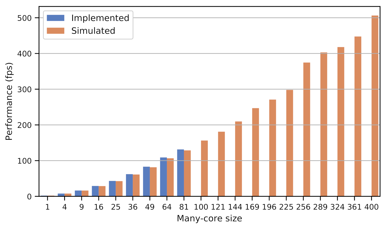
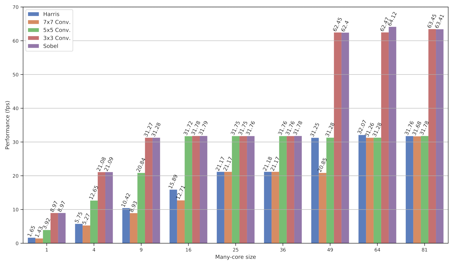
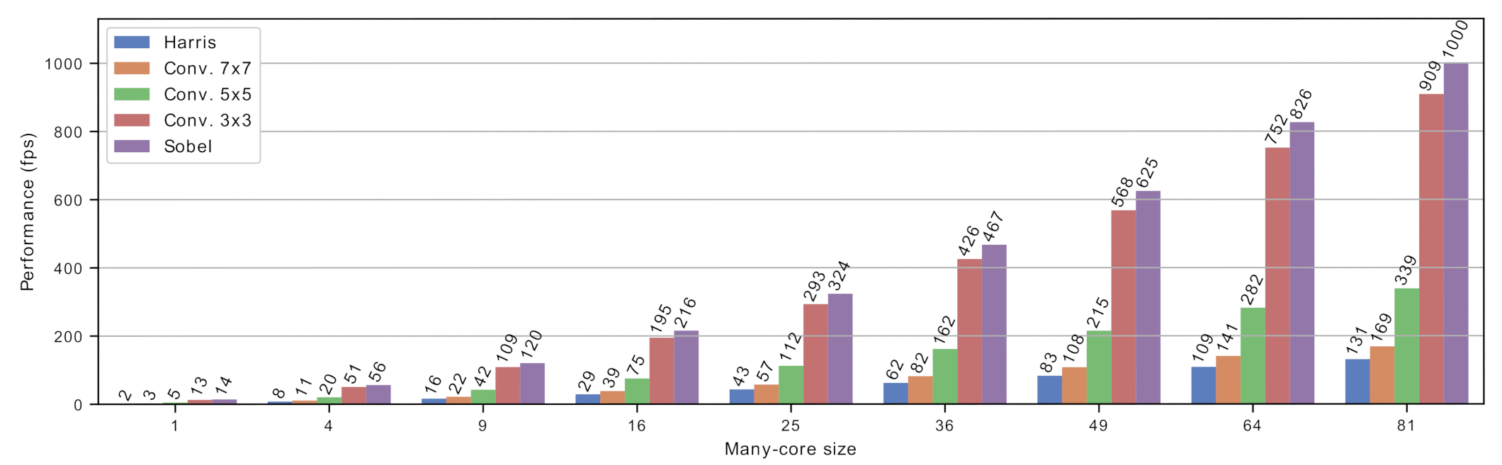
5.2. Performance Evaluation

The performance experiment was set to capture 500 frames, where the camera is set to a free-capture mode, saving all the frames in the acquisition frame buffer. The ARM processor controls the MPSoC to wait for the camera VSYNC signal and guarantee correct frame processing. As image transfer time from the acquisition FB to PMs takes about 1 ms, which is similar to the DMA transfer time, there is no pixel loss in free-capture with the camera producing 60 fps.
To determine the processing delay, the timer starts to count when the ARM finishes the setup and initialize peripherals (the MCVP, DMA, camera, and Acquisition FB) and stops to count after writing the last pixel in ARM’s DRAM through the DMA.
Five algorithms are implemented: the Harris, Sobel, 3 × 3, 5 × 5, and 7 × 7 convolutions. Figure 9 (left) shows a chessboard captured image from the sensor and read from ARM DRAM through an UART interface, for evaluation purposes. Figure 9 (right) depicts the final CoM computed over an HCD output image.
Figure 9. Left: real image acquired by the pixel sensor; right: center of mass (red cross) calculated by the ARM processor over an HCD output from the manycore.
Figure 10 shows the performance of the manycore system in simulation (up to 400 tiles) and implemented alone in the FPGA-fabric (up to 81 tiles) [4]. The implementation could reach only 81 tiles, due to the device physical limitations. However, through simulation, we can see the scalability and performance improvement by exploring the natural parallelism of the IP/CV algorithms.
Figure 10. Performance in frames per second comparing implemented and simulated results for the Harris Detector.
Figure 11 shows time performance results for the algorithms executed, from 1 to 81 PEs, in frames per second (fps) [4]. The results differ from Figure 10 due to the synchronization with the image sensor. The sensor configuration could only be used to output single-shot images (1 and 4 tiles), 30 fps (9 to 36 tiles), and 60 fps (49 to 81 tiles). The processing architecture is able to reach the performance depicted in Figure 10; however, the pixel sensor was the system’s main bottleneck. It is important to highlight that the processing architecture was designed to fulfill the real-time constraints given by the sensor frame rate.
Figure 11. Execution time for multiple algorithms with acquisition and visualization scheme.
It is not easy to compare different architecture types, as well as systems designed with different VLSI technologies. To have a kind of normalization, we computed the c y c l e s / p i x e l , which is a metric that shows how efficiently a computing architecture implements an IP/CV application. This metric is independent of the VLSI technology and the operating frequency. We believe that, with this normalization, we can fairly compare the architectural designs from several years ago until now.
A comparison, only for the Sobel edge detector against our 81 tiles implementation, is shown in Table 4 [4]. We can see that our architecture provides a good performance, while still being flexible. The authors of [20] build a method to program heterogeneous MPSoCs using the Xilinx SDSoC framework. It implements an edge detection algorithm in multiple scenarios: software only, HW/SW with static and runtime task mapping/scheduling. The authors of [12] uses a 2D mesh NoC-based 16 RISC core processor to implement different image processing tasks for its parallel programming model called threaded MPI. The authors of [19] develop a high-level synthesis tool to facilitate time-to-market heterogeneous MPSoCs design, using an MPI-based programming model and Vivado tools for HLS and TCL scripting.
Table 4. Comparison of implementations of Sobel edge detector.
Table 5 compares our best timing performance MPSoC with related architectures for the Harris corner detector application [4]. We show in the table two results: the simulated one, with 400 tiles, and the implemented one (limited by the FPGA size), with 81 tiles. The authors of [29] utilize a Jetson (ARM and GPU) similar to this work, with a GPU instead of using programmable logic. The authors of [30] implement HCD on a ASIC SIMD architecture. The authors of [12] use an NoC-based MPSoC with 16 RISC cores assisted by an external ARM CPU. The authors of [31] build the application in a processor array using VLIW PEs and point-to-point communication, building a tightly-coupled processor array. The authors of [32,33,34,35] implement pipelined HCD architectures in FPGA.
Table 5. Comparison of implementations of the HCD.
The motion estimation was implemented only in the ARM processor. Its performance is independent of the manycore’s performance, for the same input image. The center of mass computation and the motion estimation resulted in an average performance of only 1.43 ms.
In general, non-programmable pipelined FPGA architectures have better results but lack flexibility. However, other device types can also achieve similar performance, in terms of frames per second, for ICs that can run at higher frequencies but consume more power. It is important to emphasize that this work explored the platform physical limits in the Zynq ZCU104 board and still can reduce HCD execution time for larger FPGAs. Moreover, our solution brings full flexibility with a performance close to non-programmable architectures. Reference [12] is also an NoC-based MPSoC with RISC processors, and the most similar implementation to our architecture in Table 5.
The main goal of our architecture is to provide a feasible processing system for real-time IP/CV applications. A very popular architecture with similar utilization is a GPU, for example, the NVidia Jetson family [29]. Despite not being similar in the microarchitecture characteristics, we can compare our work to GPUs, considering the huge number of processing cores. We divided the comparison with GPUs into two parts: the first one with a soft GPU, and the second one with a commercial GPU.
Our manycore was implemented as an overlay architecture, so it should be fair to compare it with an overlay GPU. In [6], the authors provide the FGPU, a general-purpose GPU optimized for FPGAs. The FGPU architecture is composed of several computing units (CUs), where each CU has eight processing elements. The FGPU’s programming model is based on single-instruction multiple-threads (SIMT) and provides full-thread divergence, which means that each PE operates individually over the same program. Our manycore has the same characteristic, where each PE is independent and runs the same program. The authors in [6] benchmarked the FGPU with a varied number of CUs, as well as with a diversity of application domains. The authors connected the FGPU to an ARM processor using the AXI bus in a similar fashion to our work. The ARM was then responsible for sending data to be processed and receiving back the results. To perform this comparison, we used the ARM processor to operate in the place of our camera, resulting in a very similar testbench. Figure 12 shows the results for our testbench in different configurations, running some applications [4].
Figure 12. Performance in frames per second per architecture, all running in a testbench without a camera.
In [6], there is the benchmarking of a Sharpen filter, a convolution operation in a 5 × 5 neighborhood. For the sake of comparison, we selected their results with an eight-CUs configuration (64 PEs), the one with the highest number of PEs. Table 6 shows the comparison in its first two rows. We can see there that the manycore architecture is more efficient in parallelism exploration for the same number of PEs, reaching a higher throughput (pixels/s) with a smaller operating frequency.
Table 6. Efficiency comparison among.
The second comparison is against a commercial embedded GPU [36]. The third and fourth rows of Table 6 show the comparison. In [36], a NVidia Jetson TX2 with 256 cores runs the HCD algorithm. We compared it with our manycore with 64 PEs (4 times fewer PEs than the Jetson TX2). We can see in Table 6 that our architecture is more efficient in the parallelism exploration, with 5 × fewer cycles needed per pixel.

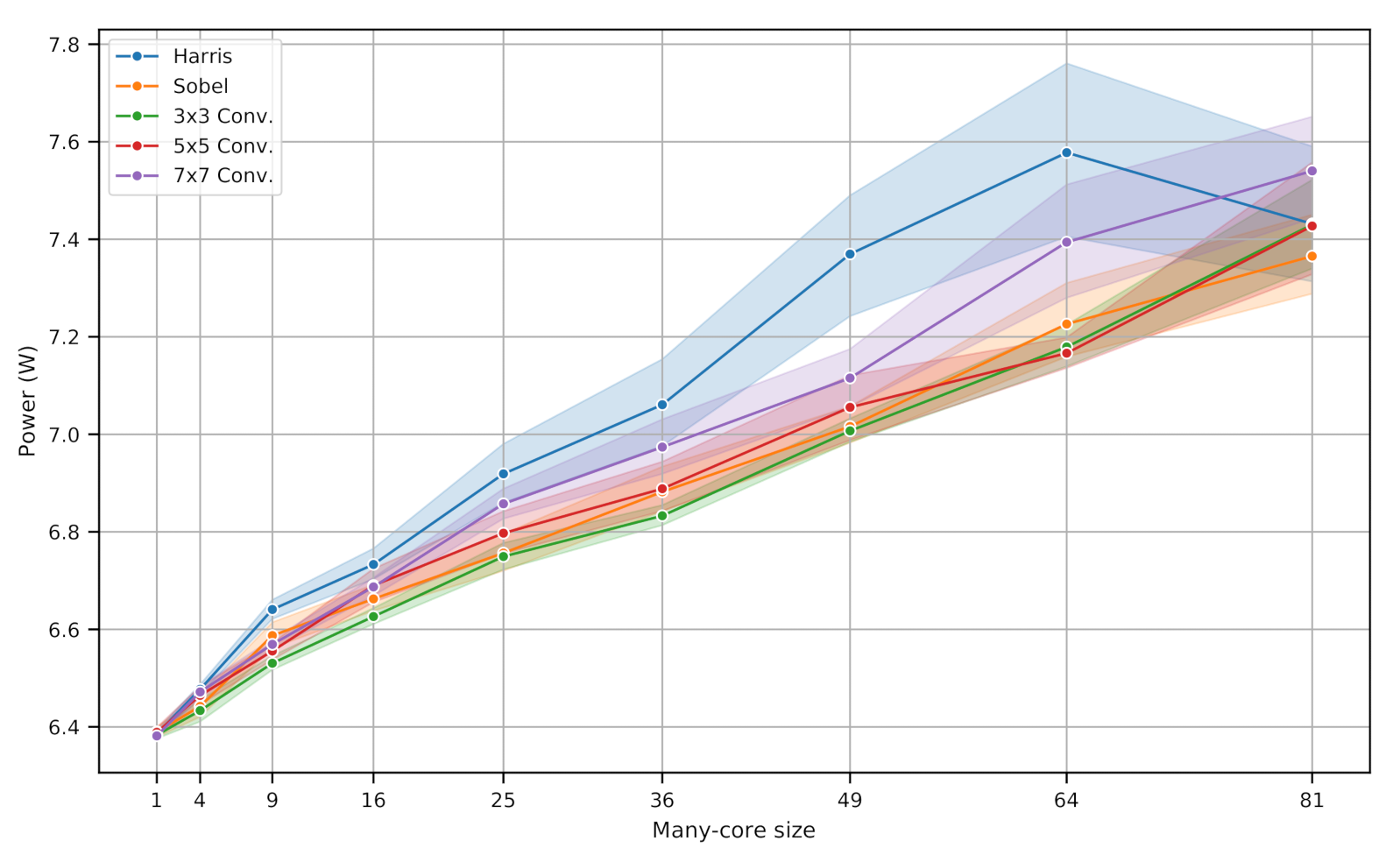
5.3. Power Consumption

The ZCU104’s power system has components to monitor voltage and current on the power rails by the Infineon manufacturer [37]. An Infineon USB005 USB cable [38] is used to obtain power results directly from a board’s specific connector.
We used the PowIRCenter GUI application to obtain power results from all rails. Considering that the ZCU104 development kit shares different peripherals in the same rail, mixing the FPGA fabric with DRAM power supply [22], for example, it is not possible to separate FPGA from ARM or other subsystems. For this reason, experimental power results concern the total instantaneous consumption in Watts (W) for all rails, including the pixel sensor. This means that the power measured is bigger than the power used by the Sensor + FPGA + ARM part.
Similarly to previous timing results, this subsection also tests the Harris, Sobel, 3 × 3, 5 × 5, and 7 × 7 convolutions, varying the number of processing frames with the algorithm and manycore size. For each algorithm, a sequence of approximately 500 images was captured to provide an average power consumption.
Figure 13 shows the power performance graphic for different algorithms and architecture sizes. Lines and points represent the measurements mean, and the shaded area is the 95% confidence interval based on the mean estimator [39]. The power behavior relates to all of the architecture components: the pixel sensor, image capture system, DMA, manycore, ARM processor, and other board subsystems.
Figure 13. Power consumed for different algorithms and architecture sizes.
With more tiles, there is more instantaneous power consumption because there are more pixel transmissions between each of them. With more routers and memory in use, the data transferences between each tile and routers’ queues occupation is less predictable. Furthermore, as we deal with a large digital system, in terms of resource usage that consumes thousands of logic units, the Flip-Flops clock distribution is not completely uniform, causing propagation delays. Combining the MCVP behavior with the FPGA and physical characteristics, the system has variable and less predictable instantaneous power consumption, leading to a standard deviation increase. As expected, the HCD takes more power to be finished since it has more operations that also take more time.

6. Conclusions

In this work, we developed a Smart Camera system based on a manycore architecture for real-time image processing and computer vision applications. The main contribution of this work is a novel manycore architecture specially designed for the IP/CV application domain. All design decisions were made considering the domain-specific needs, which resulted in a refined and efficient hardware/software architecture.
Our approach makes use of Region-based and operation level parallelism to optimize the processing time. Additionally, we designed a pixel distribution and control unit using an embedded ARM processor and AXI bus scheme. All subsystems are addressed and explained with construction details, focusing on matching application-specific needs. As a proof-of-concept, we implemented some IP/CV algorithms: the motion estimation, Harris corner detector, Sobel edge detector, and convolution filters. The results show that our architecture is capable of overcoming similar real-time architecture depending on the manycore size and application demands. The architecture is also flexible and easy to scale for higher numbers of tiles.
The manycore architecture proposed was compared to state-of-art approaches based on highly specialized FPGA implementations, reaching a good performance, while providing an application-agnostic solution. In comparison to embedded GPUs (commercial and academic ones), our solution is more efficient on parallelism exploration. GPUs are directly programmed in C/C++. Our architecture does not yet have a C/C++ compiler; however, it is almost as programmable as the GPU solutions.
In future works, we envision the utilization of a higher frame rate sensor to reach the full potential of the architecture. The proposed system is heterogeneous: we can implement the IP/CV algorithms in different architectures (direct FPGA, manycore, ARM processor). A mapping tool to obtain the algorithm description and divide it optimally over the system would also be beneficial. In addition, the other cores of the ARM processor could also be used to perform control and processing separately, as well as to run an embedded Linux operating system, bringing even more application possibilities to our Smart Camera system.

Author Contributions

Conceptualization, J.A.-G., M.H. and J.Y.; methodology, B.A.d.S., M.H. and J.Y.; codification, B.A.d.S. and A.M.L.; supervision, J.A.-G., M.H. and J.Y.; experiments, B.A.d.S., A.M.L. and J.Y.; data analysis, all authors; writing—original draft preparation, B.A.d.S., A.M.L. and J.Y.; writing—review and editing, all authors. All authors have read and agreed to the published version of the manuscript.

Funding

This study was financed in part by the following institutions: Coordenação de Aperfeiçoamento de Pessoal de Nível Superior, Brasil (CAPES)—Finance Code 001; Fundação de Apoio à Pesquisa do Distrito Federal (FAPDF); National Council for Scientific and Technological Development (CNPq).

Institutional Review Board Statement

Not applicable.

Data Availability Statement

Not applicable.

Conflicts of Interest

The authors declare no conflict of interest.

References

  1. Yudi, J.; Llanos, C.H.; Huebner, M. System-level design space identification for Many-Core Vision Processors. Microprocess. Microsyst. 2017, 52, 2–22. [Google Scholar] [CrossRef]
  2. Schmitz, J.A.; Gharzai, M.K.; Balkır, S.; Hoffman, M.W.; White, D.J.; Schemm, N. A 1000 frames/s vision chip using scalable pixel-neighborhood-level parallel processing. IEEE J. Solid State Circuits 2016, 52, 556–568. [Google Scholar] [CrossRef]
  3. Kehtarnavaz, N.; Gamadia, M. Real-time image and video processing: From research to reality. Synth. Lect. Image Video Multimed. Process. 2006, 2, 1–108. [Google Scholar] [CrossRef]
  4. Silva, B.A.; Lima, A.M.; Yudi, J. A manycore vision processor architecture for embedded applications. In Proceedings of the 2020 X Brazilian Symposium on Computing Systems Engineering (SBESC), Florianopolis, Brazil, 24–27 November 2020; pp. 1–8. [Google Scholar]
  5. Mori, J.Y.; Llanos, C.H.; Berger, P.A. Kernel analysis for architecture design trade off in convolution-based image filtering. In Proceedings of the 2012 25th Symposium on Integrated Circuits and Systems Design (SBCCI), Brasilia, Brazil, 30 August–2 September 2012; pp. 1–6. [Google Scholar]
  6. Kadi, M.A.; Janssen, B.; Yudi, J.; Huebner, M. General-Purpose Computing with Soft GPUs on FPGAs. ACM Trans. Reconfigurable Technol. Syst. 2018, 11, 1–22. [Google Scholar] [CrossRef]
  7. Hoozemans, J.; de Jong, R.; van der Vlugt, S.; Straten, J.V.; Elango, U.K.; Al-Ars, Z. Frame-based Programming, Stream-Based Processing for Medical Image Processing Applications. J. Signal Process. Syst. 2019, 91, 47–59. [Google Scholar] [CrossRef] [PubMed]
  8. Joshi, J.; Bade, S.; Batra, P.; Adyanthaya, R. Real Time Image Processing System using Packet Based on Chip Communication . In Proceedings of the National Conference on Communications, Kanpur, India, 26–28 January 2007. [Google Scholar]
  9. Joshi, J.; Karandikar, K.; Bade, S.; Bodke, M.; Adyanthaya, R.; Ahirwal, B. Multi-core image processing system using network on chip interconnect. In Proceedings of the 2007 50th Midwest Symposium on Circuits and Systems, Montreal, QC, Canada, 5–8 August 2007; pp. 1257–1260. [Google Scholar]
  10. Fresse, V.; Aubert, A.; Bochard, N. A predictive NoC architecture for vision systems dedicated to image analysis. Eurasip J. Embed. Syst. 2007, 2007, 1–13. [Google Scholar] [CrossRef][Green Version]
  11. Saponara, S.; Fanucci, L.; Petri, E. A multi-processor NoC-based architecture for real-time image/video enhancement. J. Real-Time Image Process. 2013, 8, 111–125. [Google Scholar] [CrossRef]
  12. Ross, J.A.; Richie, D.A.; Park, S.J. Implementing Image Processing Algorithms for the Epiphany Many-Core Coprocessor with Threaded MPI. In Proceedings of the 2015 IEEE High Performance Extreme Computing Conference, Waltham, MA, USA, 15–17 September 2015. [Google Scholar]
  13. Kadi, M.A. FGPU: A Flexible Soft GPU Architecture for General Purpose Computing on FPGAs. Ph.D. Thesis, Ruhr-University Bochum, Bochum, Germany, 2018. [Google Scholar]
  14. Lee, S.H.; Yang, C.S. A real time object recognition and counting system for smart industrial camera sensor. IEEE Sens. J. 2017, 17, 2516–2523. [Google Scholar] [CrossRef]
  15. Ali, K.M.; Atitallah, R.B.; Hanafi, S.; Dekeyser, J.L. A generic pixel distribution architecture for parallel video processing. In Proceedings of the 2014 International Conference on ReConFigurable Computing and FPGAs (ReConFig14), Cancun, Mexico, 8–10 December 2014. [Google Scholar]
  16. Khalil, K.; Eldash, O.; Kumar, A.; Bayoumi, M. A speed and energy focused framework for dynamic hardware reconfiguration. In Proceedings of the 2019 32nd IEEE International System-on-Chip Conference (SOCC), Singapore, 3 September 2019; pp. 388–393. [Google Scholar]
  17. Mori, J.Y.; Llanos, C.H.; Hüebner, M. A framework to the design and programming of many-core focal-plane vision processors. In Proceedings of the 2015 IEEE 13th International Conference on Embedded and Ubiquitous Computing, Porto, Portugal, 21–23 October 2015. [Google Scholar]
  18. Mori, J.Y.; Hübner, M. Multi-level parallelism analysis and system-level simulation for many-core Vision processor design. In Proceedings of the 2016 5th Mediterranean Conference on Embedded Computing (MECO), Bar, Montenegro, 12–16 June 2016; pp. 90–95. [Google Scholar]
  19. Rettkowski, J.; Göhringer, D. SDMPSoC: Software-Defined MPSoC for FPGAs. J. Signal Process. Syst. 2019, 92, 1187–1196. [Google Scholar] [CrossRef]
  20. Suriano, L.; Arrestier, F.; Rodríguez, A.; Heulot, J.; Desnos, K.; Pelcat, M.; de la Torre, E. DAMHSE: Programming heterogeneous MPSoCs with hardware acceleration using dataflow-based design space exploration and automated rapid prototyping. Microprocess. Microsyst. 2019, 71, 102882. [Google Scholar] [CrossRef]
  21. da Silva, B.A. A Manycore Vision Processor Architecture for Embedded Applications. Master’s Thesis, University of Brasilia, Brasilia, Brazil, 2021. [Google Scholar]
  22. Xilinx. HW-Z1-ZCU104 Evaluation Board (XCZU7EV-2FFVC1156)—Schematic; v1.0-rev01; Xilinx Inc.: San Jose, CA, USA, 2018. [Google Scholar]
  23. OminiVision. OV7670/OV7171 CMOS VGA (640x480) Camera Chip with OmniPixel Technology; Omnivision Technologies: Santa Clara, CA, USA, 2005. [Google Scholar]
  24. Kendri, D. FPGA Camera System. 2019. Available online: https://www.hackster.io/dhq/fpga-camera-system-14d6ea (accessed on 21 October 2020).
  25. Xilinx. Vivado Design Suite User Guide—Synthesis; Xilinx Inc.: San Jose, CA, USA, 2020. [Google Scholar]
  26. Xilinx. AXI DMA v7.1—LogiCORE IP Product Guide; Xilinx Inc.: San Jose, CA, USA, 2019. [Google Scholar]
  27. Tkg, Inc. Khronos Releases OpenVX 1.3 Open Standard for Cross-Platform Vision and Machine Intelligence Acceleration. 2019. Available online: https://www.khronos.org/news/press/khronos-releases-openvx-1.3-open-standard-for-cross-platform-vision-and-machine-intelligence-acceleration (accessed on 5 December 2020).
  28. Burger, W.; Burge, M. Digital Image Processing: An Algorithmic Introduction Using Java; Texts in Computer Science; Springer: London, UK, 2016. [Google Scholar]
  29. Chahuara, H.; Rodríguez, P. Real-time corner detection on mobile platforms using cuda. In Proceedings of the 2018 IEEE XXV International Conference on Electronics, Electrical Engineering and Computing (INTERCON), Lima, Peru, 8–10 August 2018; pp. 1–4. [Google Scholar]
  30. Hosseini, F.; Fijany, A.; Fontaine, J.G. Highly Parallel Implementation of Harris Corner Detector on CSX SIMD Architecture. In Euro-Par 2010 Parallel Processing Workshops; Springer: Berlin/Heidelberg, Germany, 2011. [Google Scholar]
  31. Sousa, É.R.; Tanase, A.; Hannig, F.; Teich, J. Accuracy and performance analysis of harris corner computation on tightly-coupled processor arrays. In Proceedings of the 2013 Conference on Design and Architectures for Signal and Image Processing, Cagliari, Italy, 8–10 October 2013; pp. 88–95. [Google Scholar]
  32. Aydogdu, M.F.; Demirci, M.F.; Kasnakoglu, C. Pipelining Harris corner detection with a tiny FPGA for a mobile robot. In Proceedings of the 2013 IEEE International Conference on Robotics and Biomimetics (ROBIO), Shenzhen, China, 12–14 December 2013; pp. 2177–2184. [Google Scholar]
  33. Liu, S.; Lyu, C.; Liu, Y.; Zhou, W.; Jiang, X.; Li, P.; Chen, H.; Li, Y. Real-time implementation of harris corner detection system based on fpga. In Proceedings of the 2017 IEEE International Conference on Real-time Computing and Robotics (RCAR), Okinawa, Japan, 14–18 July 2017; pp. 339–343. [Google Scholar]
  34. Amaricai, A.; Gavriliu, C.E.; Boncalo, O. An FPGA sliding window-based architecture Harris corner detector. In Proceedings of the 2014 24th International Conference on Field Programmable Logic and Applications (FPL), Munich, Germany, 2–4 September 2014; pp. 1–4. [Google Scholar]
  35. Possa, P.R.; Mahmoudi, S.A.; Harb, N.; Valderrama, C.; Manneback, P. A multi-resolution FPGA-based architecture for real-time edge and corner detection. IEEE Trans. Comput. 2013, 63, 2376–2388. [Google Scholar] [CrossRef]
  36. Bleijerveld, B. Harris and FAST Corner Detection on the NVIDIA Jetson TX2 Using OpenCV. Bachelor’s Thesis, University of Twente, Enschede, The Netherlands, 2019. [Google Scholar]
  37. Xilinx. ZCU104 Evaluation Board v1.1—User Guide; Xilinx Inc.: San Jose, CA, USA, 2018. [Google Scholar]
  38. International Rectifier. PowIR-USB005 User Guide; Infineon Technologies AG: Neubiberg, Germany, 2014. [Google Scholar]
  39. Waskon, M. Seaborn Lineplot (Seaborn.Lineplot). 2020. Available online: http://seaborn.pydata.org/generated/seaborn.lineplot.html (accessed on 23 January 2021).
Publisher’s Note: MDPI stays neutral with regard to jurisdictional claims in published maps and institutional affiliations.

Article Metrics

Citations

Article Access Statistics

Multiple requests from the same IP address are counted as one view.