Abstract
Infrared attenuated total reflection (ATR) spectroscopy is a common laboratory technique for the analysis of highly absorbing liquids or solid samples. However, ATR spectroscopy is rarely found in industrial processes, where inline measurement, continuous operation, and minimal maintenance are important issues. Most materials for mid-infrared (MIR) spectroscopy and specifically for ATR elements do not have either high enough infrared transmission or sufficient mechanical and chemical stability to be exposed to process fluids, abrasive components, and aggressive cleaning agents. Sapphire is the usual choice for infrared wavelengths below 5 µm, and beyond that, only diamond is an established material. The use of diamond coatings on other ATR materials such as silicon will increase the stability of the sensor and will enable the use of larger ATR elements with increased sensitivity at lower cost for wavelengths above 5 µm. Theoretical and experimental investigations of the dependence of ATR absorbances on the incidence angle and thickness of nanocrystalline diamond (NCD) coatings on silicon were performed. By optimizing the coating thickness, a substantial amplification of the ATR absorbance can be achieved compared to an uncoated silicon element. Using a compact FTIR instrument, ATR spectra of water, acetonitrile, and propylene carbonate were measured with planar ATR elements made of coated and uncoated silicon. Compared to sapphire, the long wavelength extreme of the spectral range is extended to approximately 8 μm. With effectively nine ATR reflections, the sensitivity is expected to exceed the performance of typical diamond tip probes.
1. Introduction
Infrared attenuated total reflection (ATR) spectroscopy is a common laboratory technique for the analysis of highly absorbing liquids or solid samples. When radiation in an optical material is totally reflected at an interface with a material of a lower index of refraction, part of the wave penetrates into the sample. The penetration depth of this evanescent wave, i.e., the probed sample thickness, is approximately equal to the radiation wavelength λs in the sample [1,2]. In the mid-infrared (MIR) range (3 < λ < 20 µm), this is only a few µm. The ATR technique is used in many applications, e.g., in medical diagnostics [3,4], food quality analysis [5], beverage industry [6,7], water contamination monitoring [8,9], determination of moisture in transformer and lubrication oil [10], pharmaceutical process analytics [11], and monitoring of rubber polymerization [12].
However, ATR spectroscopy is rarely found in industrial processes where inline measurements, continuous operation, and low maintenance costs are key issues. Most materials for MIR spectroscopy and especially for ATR do not have either high enough infrared transmission or sufficient mechanical and chemical stability to be exposed to process fluids, abrasive components, and aggressive cleaning agents. Up to a wavelength of 5 µm sapphire is an established material [6,7,13]. For longer wavelengths diamond is most frequently used. However, because of the high costs only very small diamond elements, e.g., tiny crystals at the tip of fiber probes, are generally used [14,15]. These diamond crystals allow only a few ATR reflections, so that the sensitivity of such arrangements is reduced compared to planar sensors with larger ATR elements and correspondingly higher number of reflections. However, rugged fiber probes with a planar diamond tip allowing multiple ATR reflections are also available and have been successfully used for process analytics in a laboratory environment [16,17]. A compact multireflection ATR setup using a diamond disk with a diameter of 14 mm and a thickness of 1 mm was recently used for the online detection of hydrogen peroxide [18].
In the laboratory, ATR crystals made of other materials like silicon, germanium, and zinc selenide are used for the longer wavelength MIR range. However, these materials are not sufficiently robust for use in industrial processes, either chemically or mechanically [19]. This is especially the case for process analytical applications in chemical and food industries. Process instruments must cope with challenging cleaning-in-place (CIP)-processes where materials in contact with process media must withstand mechanical scrubbing as well as hot water vapor and cleaning acids and bases.
Thus, for compact and cost-effective ATR process sensors a less expensive ATR material compared to bulk diamond is needed. Next to the selection of a suitable material for the ATR element, the geometry of the sensor element and packaging are also important issues to prevent fouling and enable easy cleaning of the surface [13].
In the present work, we investigated how nanocrystalline diamond (NCD) coatings on ATR elements of silicon can be realized and how sensitive and robust those process sensors for MIR-ATR measurements can become. NCD coatings can be applied to silicon substrates using an effective manufacturing process. In addition to an increased chemical and mechanical resistance of the ATR element surface, the optical properties of the diamond top layer influence the optical behavior of the entire ATR element. This effect is investigated theoretically and experimentally. Subsequently, uncoated and coated Si ATR elements are used in a process spectrometer, ATR spectra of different fluids are recorded, and the results are evaluated. Finally, the use of diamond-coated ATR elements in compact process sensors is discussed and an outlook is given.
2. Materials and Methods
2.1. Preparation and Characterization of Nanocristalline Diamond Films on Silicon
Silicon hemispheres and ATR crystals (see Table 1), obtained from Alkor Technologies, St. Petersburg, Russia, were coated with nanocrystalline diamond (NCD) films using a Hot Filament CVD process at GFD GmbH, Ulm, Germany. Typical HFCVD process parameters using CH4 and H2 as main reaction gases were: substrate temperatures 750–900 °C, filament temperatures: 1900–2200 °C, chamber pressure 1–20 mbar, and growth rates 50–400 nm/h. Optimizing the process parameters, homogeneous NCD films with a thickness up to several µm were obtained. Further details on the HFCVD process can be found in the literature, e.g., [20,21].

Table 1.
Silicon hemispheres (radius 12.5 mm) and silicon ATR crystals (50 mm × 10 mm × 2 mm; the short faces are wedged at a 45° angle). The thickness data of H1, H2 were optically determined by IPM. Data for C1, C2 were reported by the manufacturer based on the coating process parameters. Due to the spatial inhomogeneity of the coatings (see Figure 7b), a 10% uncertainty is assumed for all coating values.
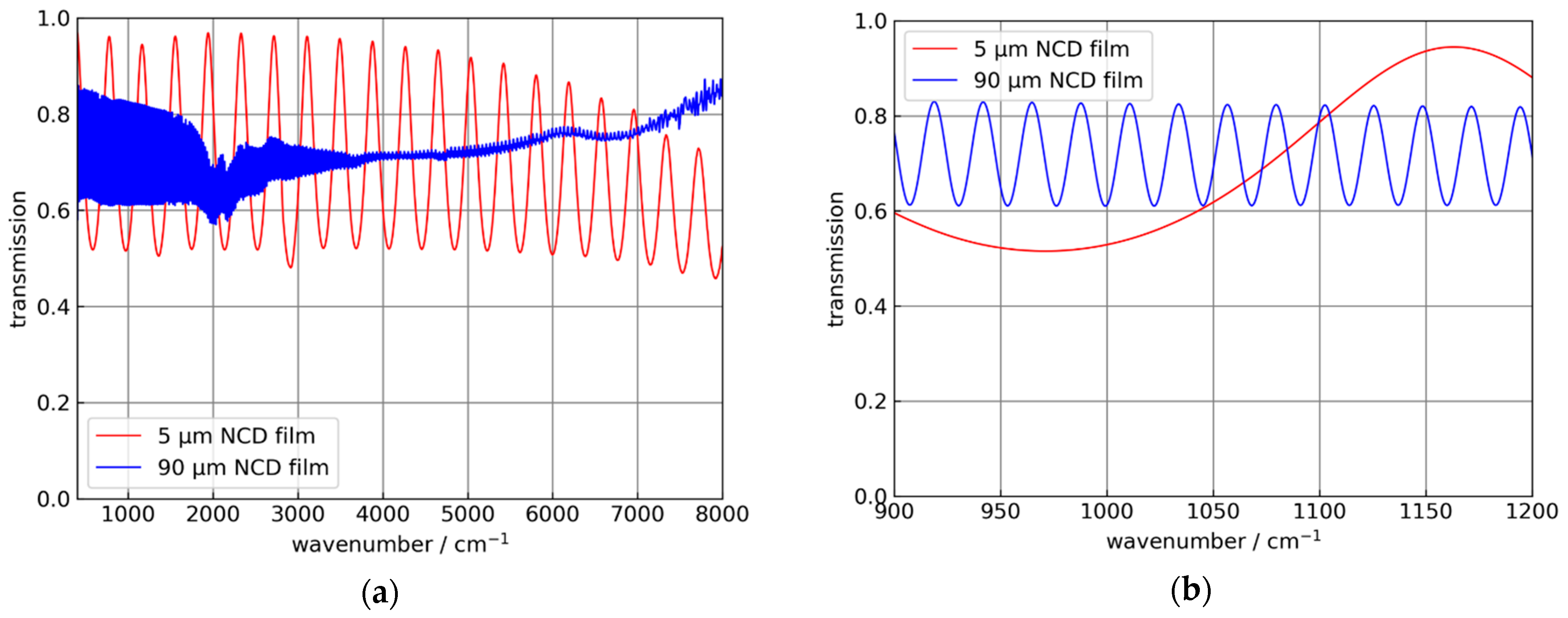
In the following, for the Si hemispheres and the Si ATR crystals a refractive index of 3.43 for Si in the MIR spectral range was used [22]. For the NCD films, a value of 2.38, which is typical for CVD-diamond materials, was used [23,24]. This value was confirmed by infrared transmission measurements of freestanding NCD films with 5 and 90 µm thickness, respectively, measured with a Bruker Vertex 80V FTIR spectrometer (Bruker Optik GmbH, Ettlingen, Germany), and shown in Figure 1.
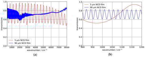
Figure 1.
Transmission measurements of “thick” NCD films, which were used to determine the effective refractive index of the material. (a) Infrared transmission of 5 and 90 µm thick NCD films. (b) Detail showing the interference fringes of the 90 µm thick NCD film with higher resolution.
For process applications, the coating on a Si ATR surface must not have any defects. For that reason, exemplary tests were performed by GFD: Visually defect-free NCD-coated Si samples were exposed to concentrated KOH, which is an established etching solution for Si. After rinsing and drying, the NCD coating was removed by an O2 plasma etching process. The formerly coated Si surface was then inspected for the occurrence of any etch pits by optical and scanning electron beam microscopy. In the case of pinholes in the NCD coating, such etch pits at the interface would have been formed by KOH intrusion. However, for NCD films with a thickness >300 nm no etch pits were observed, indicating that the original NCD coating was pinhole-free.
Additionally, the suitability of NCD-coated Si elements for applications in the beverage industry was investigated by CENTEC GmbH, Maintal, Germany. Uncoated and NCD-coated Si elements were exposed to 5% v/v NaOH solutions at 80 °C, 3% v/v HNO3 solution at 40 °C, and several beverages.
Subsequent visual inspection showed that the coated sides of the samples were not affected by the agents. Uncoated Si surfaces were not stable.
2.2. Theoretical Background and Simulation
2.2.1. Attenuated Total Reflection (ATR)
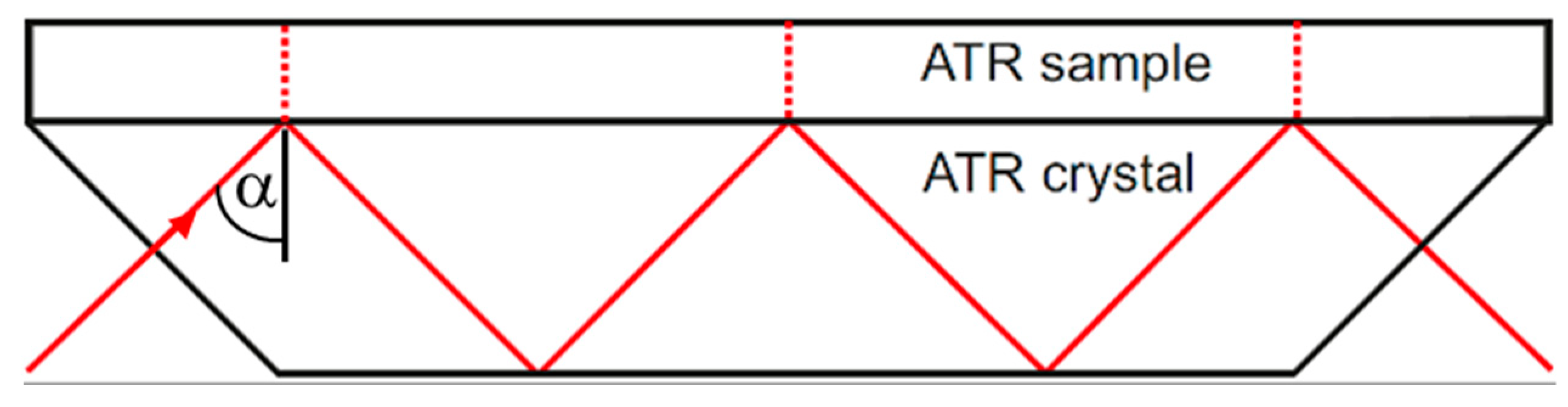
The basic principles of the effect of attenuated total reflection (ATR) are explained in many textbooks, e.g., Harrick [2]. A typical configuration for multireflection ATR is shown in Figure 2. The angle of incidence α is higher than the critical angle αc, so that the wave is totally reflected at the interface.
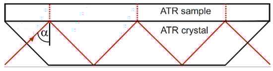
Figure 2.
Typical ATR multireflection configuration.
In the ATR crystal, a standing wave is generated and because of the boundary conditions, the electromagnetic field decays exponentially into the sample. This field is called the evanescent field.
The critical angle αc can be defined as follows [25], where n1 and n2 are the real parts of the refractive indices of ATR crystal and sample, respectively.
Because of the electromagnetic continuity conditions, the wave intrudes into the sample and decays exponentially. The penetration depth dp is defined as the distance from the interface when the amplitude of the evanescent wave is decreased to 1/e of the amplitude at the interface [25].
Typically, the penetration depth of the evanescent wave is in the range of the wavelength λ of the radiation used. The wavelength-dependent absorption of the evanescent wave inside the sample leads to an attenuation of the reflected beam. By measuring the spectral dependence of the reflected beam intensity, an ATR spectrum is obtained.
For a standard transmission measurement, one obtains for the transmission factor T according to Beer’s law:
where I0 is the initial intensity, I denotes the intensity after passing the sample with the thickness d, k is the optical extinction coefficient, and a describes the absorption coefficient of the sample. With k, the complex refractive index n of a material can be expressed as:
This also allows us to define the important term of absorbance:
The absorbance A is a dimensionless quantity. However, in spectroscopy the AUs (absorbance units) and milli-absorbance units (mAUs) are commonly used. Throughout this paper we use this convention.
Compared to transmission spectroscopy, ATR spectroscopy has some special characteristics: the strength of the absorbance also depends on parameters such as incidence angle and the refractive indices of ATR material and sample.
Analogous to transmission spectroscopy, the effective penetration depth de can be defined for ATR spectroscopy [25]. It describes the path length through the sample that is necessary to produce the same absorbance in a transmission experiment:
where R describes the polarization-dependent reflection factor. For uncoated ATR crystals it is calculated in a straightforward way using the Fresnel equations [25]. By analogy to Equation (5), the absorbance for ATR measurements is obtained:
The extension for coated ATR crystals is shown in Section 2.2.2. The use of a multireflection configuration as in Figure 2 linearly increases the absorbance by the number of reflections.
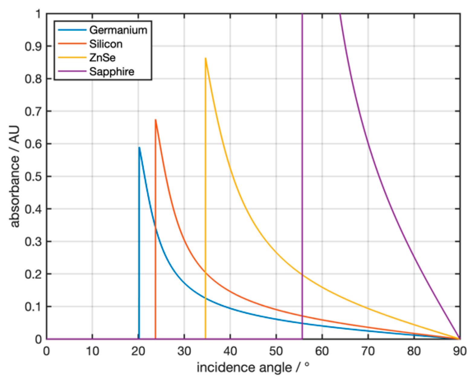
Figure 3 shows the theoretically calculated, angle-dependent absorbances for different ATR crystal materials and a water sample for a single reflection of infrared radiation at 3300 cm−1 (corresponding to the strong absorption band of water). The complex refractive index of the sample is 1.404 + 0.253i [26]. The simulation shows that both the crystal material and the angle of incidence have a strong influence on the absorbance.
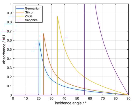
Figure 3.
Theoretical absorbance of water at 3300 cm−1 for the ATR materials germanium, zinc selenide, sapphire, and silicon.
2.2.2. Simulations for ATR Elements with a Coating Layer
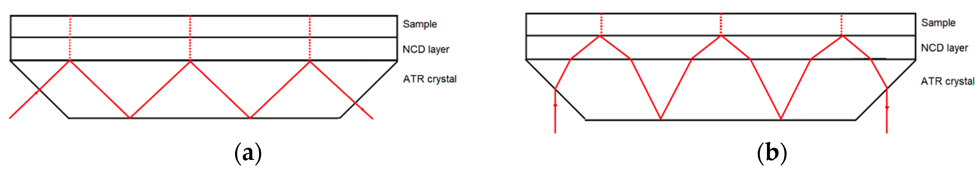
The ATR effect is strongly changed by a covering layer on the ATR element. The optical properties of the coating material, the coating thickness, and the angle of incidence influence the measured absorbance of a sample. In the following, these influences for NCD layers on silicon are described by theoretical calculations. Depending on the incidence angle α, two different scenarios are possible (see Figure 4).
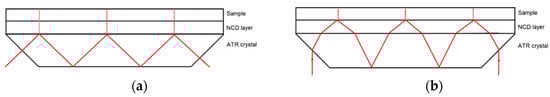
Figure 4.
(a) Scenario 1: total internal reflection at the interface between ATR crystal and coating layer. A 45° wedged element with perpendicular incidence is shown. (b) Scenario 2: total internal reflection at the interface between coating layer and sample. To achieve a smaller incidence angle at the Si–NCD interface a 45° incidence angle at the air–Si interface is shown. The dimensions do not have the same scale.
In scenario 1, the incident radiation is totally reflected at the interface between ATR crystal and diamond coating. Thus, the electromagnetic field in the diamond coating and in the sample is evanescent. According to Equation (1) for NCD layers on Si, this is the case for incident angles at the Si–NCD interface α ≥ 44°. In scenario 2, the incident wave intrudes into the diamond coating and is totally reflected at the interface between diamond coating and sample. In this case, the evanescent field is only present in the sample. According to Snell’s law and Equation (1) for NCD layers on Si and a water sample this is the case for incident angles at the Si–NCD interface 23° < α < 44°.
Subsequently, it is interesting to investigate the influence of an NCD coating on the absorbance of the ATR measurement. The coating leads to an increase or decrease of the absorbance caused by interferences in the coating. The absorbance for scenario 1 can be determined by using numeric simulation software, e.g., the Lumerical 3D/2D Maxwell’s Solver for Nanophotonic Devices [27].
In the following, only scenario 2 is considered, in which the absorbance is calculated analytically using Equation (7). However, the reflection factor R for a coated ATR system is different from the reflection factor of an uncoated ATR system. The corresponding equations can be found in [28]. In Figure 5, the calculated absorbances of an uncoated Si ATR crystal and a Si ATR crystal with a 500 nm thick NCD coating are shown for the strong water absorption band at a wavenumber of 3300 cm−1. For the refractive indices of silicon, diamond, and the sample, the values 3.43 [22], 2.38 [23,24], and 1.404 + 0.253i [26] are used, respectively.
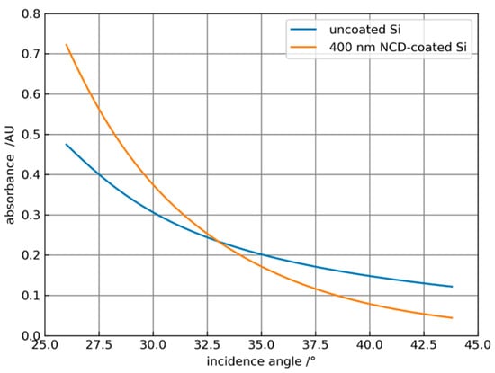
Figure 5.
Dependence of the water absorbance at 3300 cm−1 on the angle of incidence for uncoated Si and NCD-coated Si with a thickness of 400 nm.
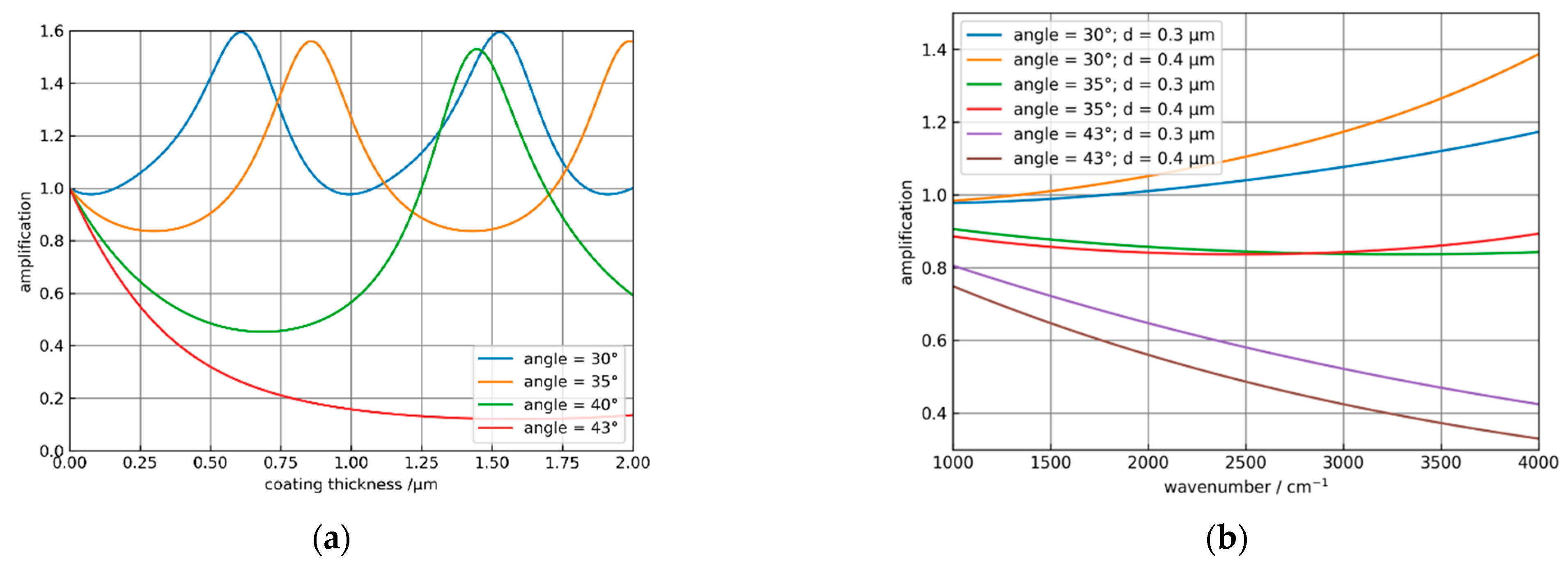
Obviously, the coating leads to an amplification of the absorbance for angles smaller than 33°. As the angles increase, the decrease in the absorbance of the coated system is stronger than for the uncoated element. In Figure 6a the amplification = absorbancecoated/absorbanceuncoated is plotted against the coating thickness of the ATR crystal for different incidence angles for water with the same parameters, as in Figure 5. Obviously, it is possible to optimize the coating thickness for a specific angle of incidence or vice versa to maximize the amplification. Figure 6b shows the spectral dependence of the amplification for the solvent propylene carbonate (PC) with an index of refraction of 1.41 for different angles of incidence and 300 and 400 nm thick NCD coatings. Here, amplification is only possible at an angle of 30° and increases toward higher wavenumbers. For α > 35° an increasing attenuation is calculated. Corresponding measurements of ATR spectra of PC are reported in Section 3.2.
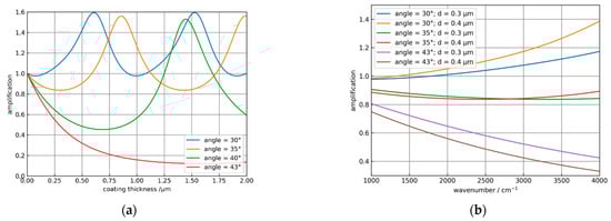
Figure 6.
(a) Dependence of the amplification on the coating thickness for water at 3300 cm−1 and incidence angles α of 30°, 35°, 40°, and 43°. (b) Spectral dependence of the amplification for α = 30°, 35°, and 43° and two different NCD coating thicknesses for propylene carbonate (PC).
2.3. Experimental ATR Setup Using Si Hemispheres
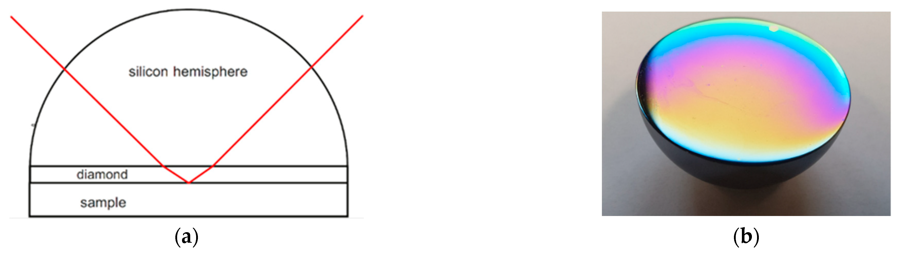
To perform variable-angle ATR spectroscopy, a “Seagull” ATR accessory setup (Harrick Scientific Inc., New York, NY, USA) was attached to a Bruker Vertex 80V FTIR spectrometer (Bruker Optik GmbH, Ettlingen, Germany). With this setup it was possible to set the angle of incidence in a range between 5° and 85°. The ATR elements were hemispheres in order to use this range of possible angles. In Figure 7a the optical path in such a hemispherical ATR crystal is shown. Figure 7b shows the planar surface of a coated silicon hemisphere. The thin-film interference indicated that the coating thickness was not uniform. Since the optical beam was mainly reflected at the center of the basal plane predominantly the coating thickness at the center was relevant for the measurements. The coating thickness can be determined from the interference pattern of, e.g., a normal incidence transmission or reflection spectrum. With respect to film inhomogeneity a 10% uncertainty of the thickness determination was estimated.
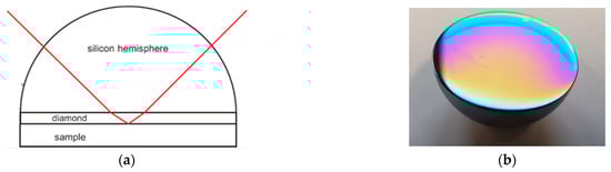
Figure 7.
(a) Optical path in a hemispherically shaped and NCD-coated ATR element. The diamond layer is shown enlarged for visibility. (b) Image of an NCD-coated Si hemisphere.
2.4. Experimental ATR Setup Using Planar Si ATR Elements
With the “Seagull” setup, only one ATR reflection can be realized. Planar ATR elements with multiple reflections (as sketched in Figure 2) can be used to provide a larger absorbance signal for a given sample. This is important for process applications, where a more compact and robust design is required, and measurements are generally performed using a fixed incidence angle.
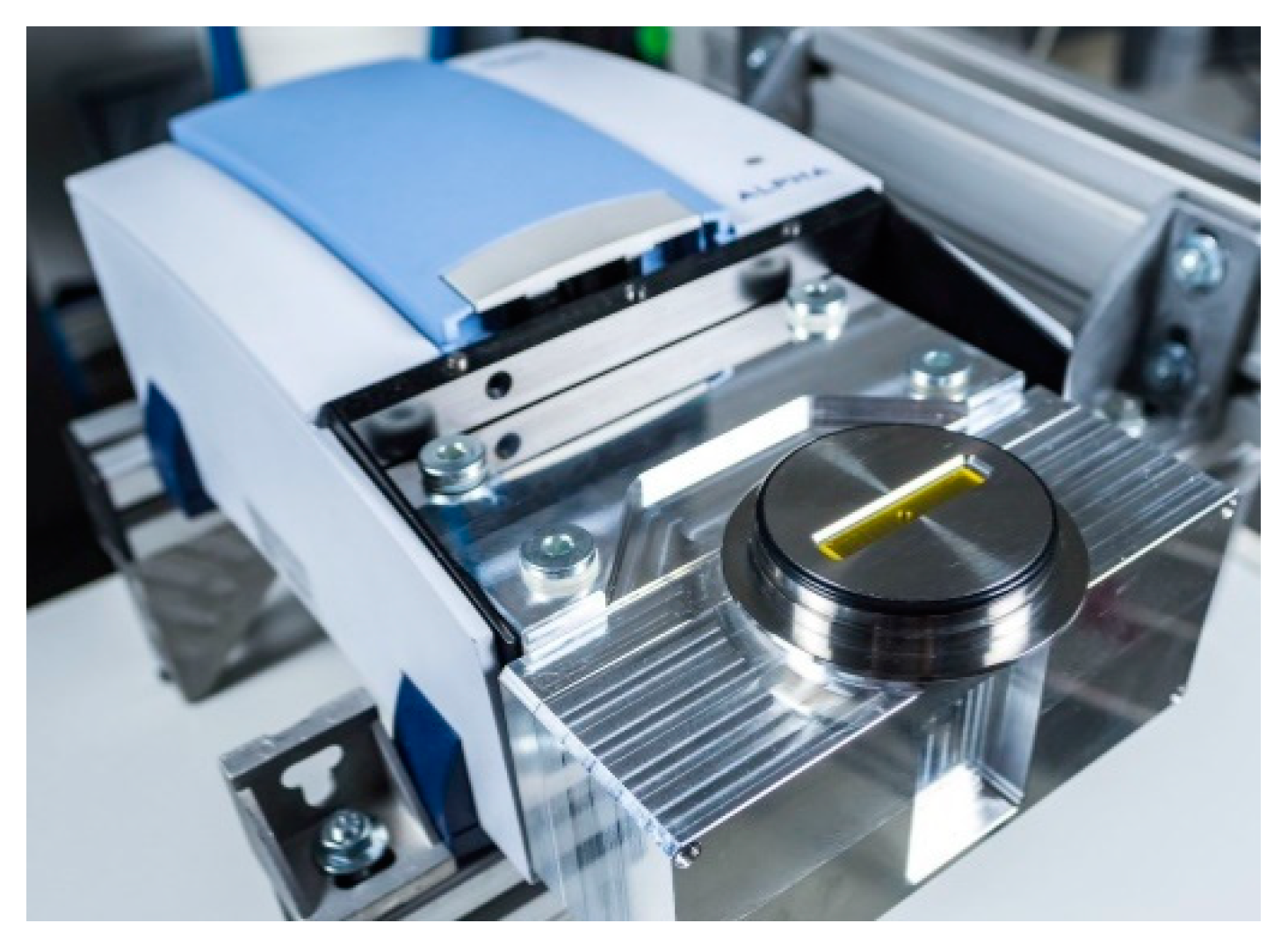
Therefore, planar Si ATR elements with a 45° wedge for radiation in- and outcoupling (see Table 1) were mounted into a Varivent flange, which is frequently used for instrumentation in the beverage industry. Figure 8 shows how the flange was coupled to an Alpha FTIR spectrometer (Bruker Optik GmbH, Ettlingen, Germany). With such ATR elements, 11 ATR reflections can be achieved nominally. Furthermore, other ATR materials such as sapphire or ZnSe can be easily mounted into the Varivent flange for comparison [13]. Results of the spectroscopy measurements with the planar Si ATR elements C0, C1, C2 are reported in Section 3.2.

Figure 8.
Planar ZnSe-ATR element with Varivent flange coupled to a Bruker Alpha FTIR instrument.
The entire unit (flange and spectrometer) can be coupled to a process line for continuous operation. Alternatively, the Varivent flange assembly may be coupled to a compact photometer or micro-spectrometer module to realize a compact process sensor [13]. Such a sensor with a sapphire ATR element is available, for example, from CENTEC GmbH, Maintal, Germany, to measure the CO2 content in beverages [7].
3. Results
3.1. Results from Uncoated and NCD-Coated Hemispheres
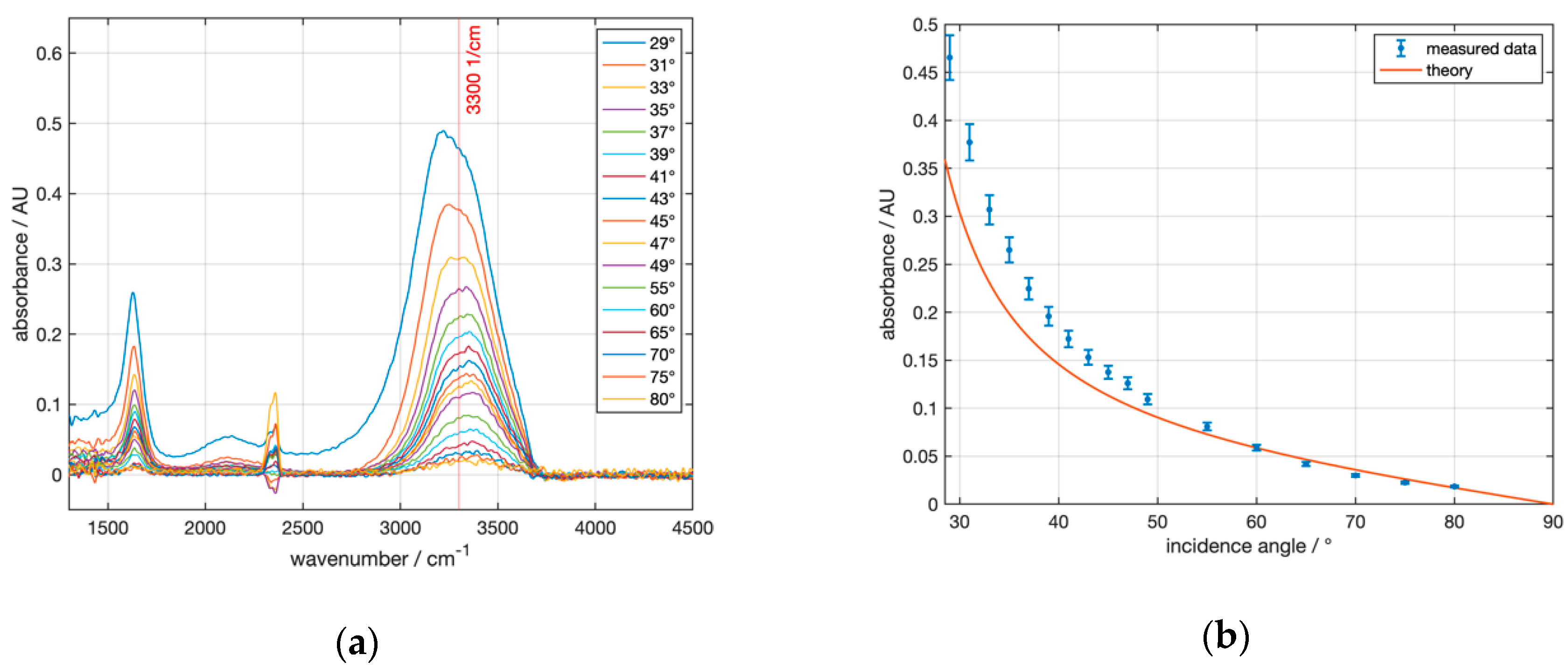
With the “Seagull” setup, angle-dependent ATR measurements with uncoated and coated silicon ATR crystals H0, H1, H2 were performed. Figure 9a shows the absorbance of water measured with the uncoated hemisphere H0 at angles of incidence of 29° and above. The distinct water absorption band at 3300 cm−1 is clearly visible.
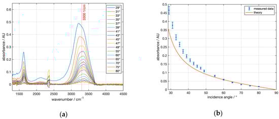
Figure 9.
ATR absorbance spectra of water recorded with the Seagull setup using the Si hemisphere H0 with varying angles of incidence. (a) shows the water absorbance spectra with reference to air at the respective angle, smoothed by a moving average filter and offset-corrected to 4000 cm−1. (b) compares the angle-dependent absorbance values at 3300 cm−1 to theoretical values.
Qualitatively, there was a fair agreement of the experimental data with the model calculation in Figure 3 for uncoated Si. Figure 9b shows that almost all measured absorbances were above the theoretically predicted values. These deviations became very large, especially at small angles, i.e., close to the critical angle. One possible reason is that close to the critical angle, owing to the divergence of the infrared beam, a considerable portion of the radiation was lost by transmission, resulting in a reduced intensity of the reflected beam and, hence, an apparently increased absorbance.
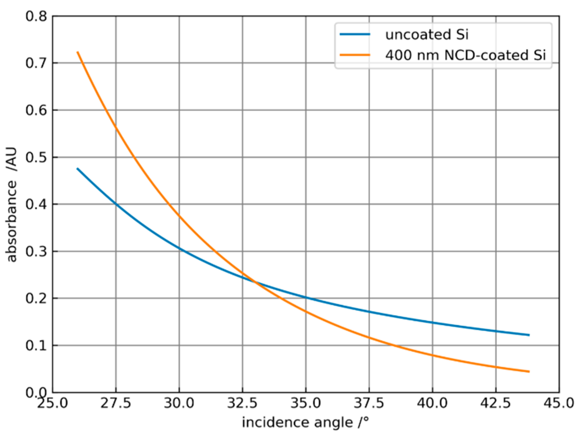
The experimental results of the angle-dependent ATR measurements of the water absorption band at 3300 cm−1 with NCD-coated silicon hemispheres are shown in Figure 10a for water as a sample. For angles of 29° < α < 34° an increase in the absorbance compared to H0 was observed for hemisphere H1. For hemisphere H2 no amplification effect was observed. Above an angle of 34°, however, the absorbance of both diamond-coated silicon hemispheres H1 and H2 was lower than for H0. In Figure 10b the measurement was repeated with the solvent propylene carbonate (PC) at a strong absorption band at 1782 cm−1. Here, diamond coating led to an attenuation of the absorption for all angles. The attenuation increased at larger angles.
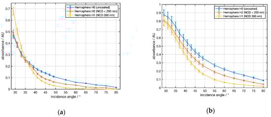
Figure 10.
Experimentally determined angular dependence of the absorbance for silicon as ATR material and two NCD coatings with two samples: (a) water at a wavenumber of 3300 cm−1 and (b) propylene carbonate at a wavenumber of 1782 cm−1. Data points are connected by lines to guide the eye.
To compare the experimental observations shown in Figure 10 with the theoretical results (Figure 5 and Figure 6) selected data are shown in Table 2. For water at 3300 cm−1 the experimental value of the amplification exceeded the result of the simulation at all angles. For PC @ 1781 cm−1 the simulation predicted a small amplification at 30° that was not observed in the experiment. However, for 35° and 43° the simulation fit well to the measured data.
Regarding the inhomogeneity and the estimated 10% uncertainty of the thickness of the NCD films the experimental data gave a qualitative confirmation of the calculated angular dependence of the amplification in both settings.
3.2. Results with Planar ATR Elements
With the setup described in Section 2.4, measurements with planar uncoated (C0) and coated (C1, C2) Si elements were performed. Sample liquids were dripped onto the surface of the ATR elements. To prevent evaporation of the liquid the wet surfaces were covered with microscope lids during the measurements.
3.2.1. ATR Spectra of Water
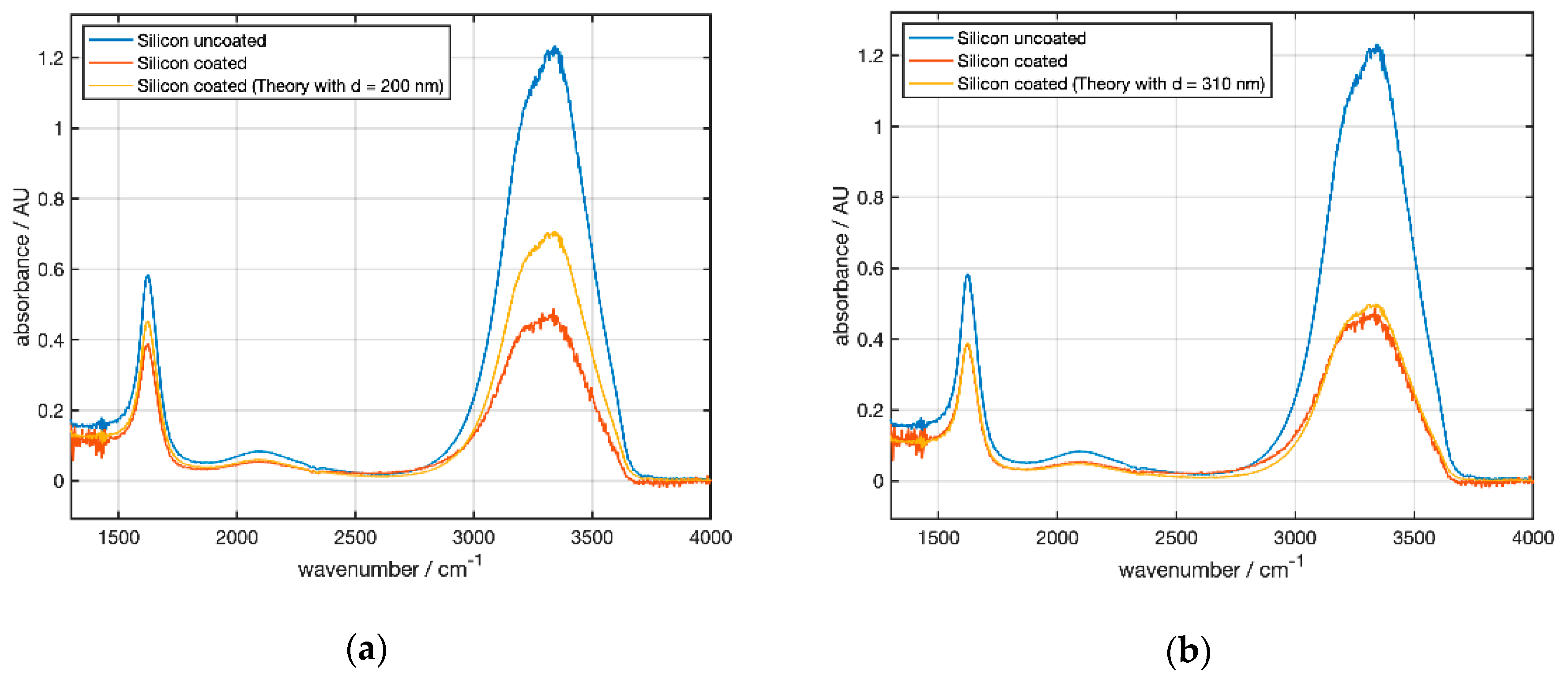
Figure 11a gives an absorbance of 1.23 at 3300 cm−1 compared to 0.14 for the uncoated hemisphere C0 at an angle of 45° (Figure 10a), which is a factor of 8.8 because of multiple reflections.
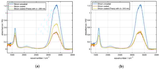
Figure 11.
ATR spectra at 45° for water measured with the alpha spectrometer. Blue curve: measurement of uncoated Si Element C0. Red curve: measurement of coated element C1. The orange curve shows a simulated spectrum obtained by multiplication of the blue curve by a wavelength-dependent attenuation factor. (a) A coating thickness of 200 nm is used for the simulation. (b) Using a coating thickness of 310 nm an optimum fit of simulated and measured spectra is obtained.
According to Figure 10 one would expect an attenuation of the absorbance for a 200 nm thick NCD coating to ≈ 0.4 at 3300 cm−1 (see Table 3). Figure 11a shows that for C1 both peaks (3300 and 1600 cm−1) showed a smaller absorbance than the simulation for a layer thickness of 200 nm. This indicated that the real layer thickness was larger than reported by the supplier (see Table 1). Extrapolating the simulated spectral dependence of the attenuation factor (Figure 6b) to 45° allowed us to adjust the coating thickness. The best agreement was obtained for 310 nm (Figure 11b).
Table 3.
Peak absorbance values for uncoated and coated Si hemispheres at 45° incidence angle (data from Figure 10).
The increased noise below 1500 cm−1 was caused by low transmission of the Si substrates because of intrinsic absorption. At 3300 cm−1 noise resulted from low transmission owing to the strong liquid water absorption. Additionally, atmospheric water vapor in the setup had sharp absorption lines between 3300 and 4000 cm−1, which also contributed to the measured spectra.
3.2.2. ATR Spectra of Acetonitrile and Propylene Carbonate
For further investigations, solutions of acetonitrile (AC) in propylene carbonate (PC) were used. To study the feasibility of an ATR setup, spectroscopy of AC solutions is an alternative to pressurized dissolved CO2, which is important for the beverage industry and to toxic isocyanates, which are key chemicals with high-volume production worldwide [13]. Acetonitrile has a strong absorption at 2252 cm−1.
Additionally, propylene carbonate has a strong absorption band at 1782 cm−1, which is out of reach of the frequently used sapphire ATR elements. AC and PC are miscible liquids.
The results of the measurements of AC in PC solutions for uncoated and NCD-coated Si ATR elements are shown in Figure 12 and Figure 13.
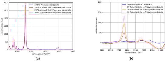
Figure 12.
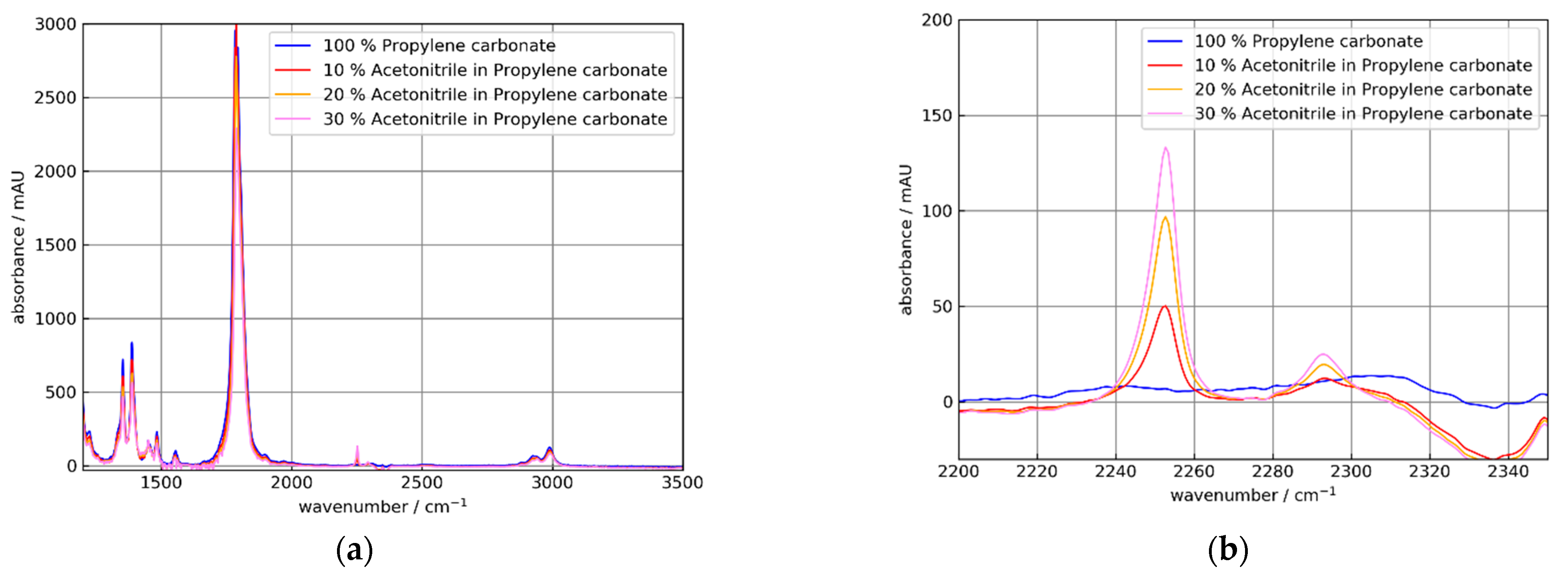
Absorbance spectra of 0, 10, 20, und 30% m/m solutions of acetonitrile (AC) in propylene carbonate (PC) using the uncoated Si ATR element C0. The absorbance spectra were referenced to air. (a) Broad spectral range showing strong PC absorption at 1782 cm−1 and relatively weak AC absorption at 2250 cm−1. (b) Detail showing AC absorption bands at 2250 and 2292 cm−1. The apparent negative absorption at 2340 cm−1 is an artifact caused by gaseous CO2 in the optical path.
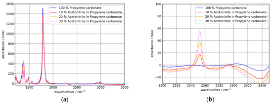
Figure 13.
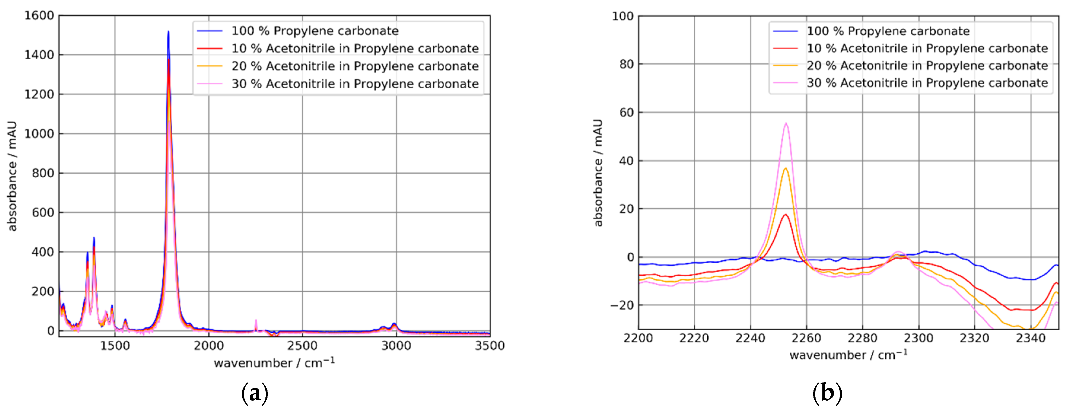
Absorbance spectra of 0, 10, 20, und 30% m/m solutions of acetonitrile (AC) in propylene carbonate (PC) using the Si ATR element C2. (a) Broad spectral range showing strong PC absorptions at 1388 and 1782 cm−1 and a weak AC absorption at 2250 cm−1. (b) Detail showing acetonitrile absorption bands at 2250 and 2292 cm−1. The absorbance spectra were referenced to air. The apparent negative absorption at 2340 cm−1 is caused by gaseous CO2.
As expected from Figure 10, the absorbance for the coated crystal C2 was smaller than for the uncoated element C0. Additionally, the AC absorbance increased approximately linearly with the AC concentration. Respectively, the PC peak decreased similar to the PC concentrations. For further discussion, the peak absorbance data are collected in Table 3 and Table 4.
4. Discussion
It was shown that NCD-coated Si elements can serve as suitable materials for ATR process sensors. A thickness larger than approximately 300 nm was sufficient to ensure long operation time and stability of the surface sensor against cleaning agents. Compared to commonly used sapphire elements the long wavelength extreme of the spectral range was extended to approximately 8 µm.
Additionally, the results from Si hemispheres showed that with an angle of incidence of less than 34° and a suitable coating thickness, an amplification of the absorbances compared to uncoated Si elements could be achieved.
At larger angles of incidence, coating resulted in absorbance attenuation. For the strong water peak at 3300 cm−1, the data in Table 3 yield absorbance ratios of 0.61 for H2/H0 and 0.37 for H1/H0 as a result of the thicker coating of H1. The corresponding ratio for C1/C0 in Table 4 from Figure 11 is 0.38, indicating that the NCD thickness value reported by the manufacturer was too low. Experimental data were best fit by simulations assuming a layer thickness of 310 nm. Additionally, both absorbance ratios for water and PC in Table 3 fit well to the calculations in Figure 6a,b.
Comparing the water absorbances of the ATR crystals and the hemispheres yielded C0/H0 = 8.78, clearly showing the absorbance increase by multiple reflections. For the coated elements, a similar value of C1/H1 = 9 was obtained. This effective number of reflections was lower than the geometrically determined reflection number of 11 for the 45° elements. This discrepancy was attributed to intrinsic absorption, beam divergence, and scattering effects in the ATR element. (The strong PC absorbance at 1782 cm−1 saturation for the C0 signal reduced the value to ≈7).
A closer look at the data in Table 4 showed that the absorbance ratio of coated to uncoated Si elements C2/C0 moderately decreased from ≈0.6 at 1388 cm−1 to ≈0.4 at 3300 cm−1 within the experimental uncertainties (e.g., saturation effects for the strong PC absorption band at 1782 cm−1 and baseline corrections). This observation agreed qualitatively with the calculation in Figure 6b.
The absorbance increase at 2252 cm−1 with the AC concentration was slightly nonlinear. This was expected from previous work [13]. A similar behavior was found for the corresponding decrease of the PC peaks with increasing AC concentrations.
To indicate the potential of such diamond-coated Si ATR elements the following line of argument may be used: since ZnSe and diamond have almost the same MIR indices of refraction, for a bulk diamond crystal with identical dimensions the same absorbance is expected. Using a ZnSe element, ATR spectra of mixtures of AC in isopropanol were measured in [13] using the same FTIR setup with 11 reflections. There, for a 20% m/m mixture an absorbance of 155 mAU was determined, i.e., 14 mAU per reflection. Thus, for a diamond probe with two reflections one would expect 28 mAU.
With the NCD-coated Si element C2 a value of 44 mAU for a 20% m/m mixture of AC in PC (see Table 3) was obtained. Thus, with nine effective reflections a higher sensitivity than a diamond tip probe with two reflections were achieved.
Making use of the amplification effect by selection of an incidence angle of, e.g., 30° and a coating thickness of 0.5 µm would yield higher single reflection absorbance and an increase in the number of reflections. This would clearly outperform the sensitivity of a diamond tip probe.
5. Conclusions and Outlook
As a result, NCD-coated Si elements may be used in typical ATR accessories for FTIR instruments when a higher mechanical and/or chemical resistance of the surface is required. This is especially the case when using a compact FTIR instrument in a process environment.
Furthermore, the advent of compact MIR FPI micro spectrometers [29] opens the way for palm-sized process spectrometers using coated planar Si ATR elements as a cost-effective alternative to bulk diamond ATR crystals. By optimizing the angle of incidence and using suitable AR coatings for the entrance and exit faces of the Si ATR element, a substantially higher sensitivity can be expected owing to the high number of reflections.
Photometric detection is another possibility to realize a compact and robust process sensor as described, e.g., in Lambrecht et al. [13] and Theuer et al. [30]. A further step toward miniaturization is the use of MEMS technologies, as described in De Graaf et al. [31]. Radiation sources and thermopile detector elements can be fabricated using Si MEMS technology on a first wafer. A second Si wafer with the coated ATR element can then be bonded to the first wafer. The entire unit can be hermetically sealed in a compact housing, similar to infrared detector packages. A major advantage of using Si as an ATR element is that the processing and packaging steps are well established and ready for scale-up to high production volumes.
First experiments using such MEMS-integrated devices showed the feasibility of this approach. This topic will be further investigated. Although in several process applications the thermal and mechanical constraints will not allow inline use of such devices, there are still many applications left for cost-effective ATR sensors that can be fabricated in substantial volumes. Possible applications currently performed with FTIR transmission spectroscopy include, e.g., quality control of lubricating oil [32] or milk analysis [33]. Compact ATR sensors can be used for fast at-line analysis and can also be incorporated into handheld instruments.
Instead of using nanocrystalline diamond films as coating material, DLC coating could be an alternative [34]. Our first experiments with DLC-coated Si ATR elements showed that similar results can be obtained and that sufficient mechanical and chemical resistance of the DLC coating can be achieved. A major advantage of DLC is that coating on Ge ATR elements can be realized. Until now, diamond coating on Ge with the HFCVD process was only possible with a metallic bonding layer, which is detrimental for optical applications. Optimization of DLC-coated Ge ATR elements can be performed in a similar way to Si. With DLC-coated Ge an even broader spectral range and access to the MIR fingerprint range for robust, cost-effective, and compact ATR process sensors is foreseeable.
Author Contributions
Conceptualization, N.A., F.K. and G.S.; Theoretical description, N.A., F.K.; Measurements, N.A.; Methodology, G.S., F.K. and A.L.; Data analysis, N.A., C.B. and A.L.; Writing, N.A. and A.L. All authors have read and agreed to the published version of the manuscript.
Funding
This work was funded by the German Ministry of Education and Research (BMBF), grant No. FKZ 13N14577.
Acknowledgments
We gratefully acknowledge the support of our project partners GFD GmbH for supplying the NCD coatings and characterization, CENTEC GmbH for measurements of the chemical resistance in cleaning agents, and Micro-Hybrid GmbH for supplying us with first samples of DLC-coated elements and packaged sensors. Special thanks to our colleagues at IPM Ulrich Ulmer and Jochen Erb for mechanical design and construction.
Conflicts of Interest
The authors declare no conflict of interest. The founding sponsors had no role in the design of the study; in the collection, analyses, or interpretation of data; in the writing of the manuscript, and in the decision to publish the results.
References
- Harrick, N.J. Electric Field Strengths at Totally Reflecting Interfaces. J. Opt. Soc. Am. 1965, 55, 851–856. [Google Scholar] [CrossRef]
- Harrick, N.J. Internal Reflection Spectroscopy, 3rd ed.; Harrick Scientific Corporation: New York, NY, USA, 1987; ISBN 0-933946-13-9. [Google Scholar]
- Heise, H.M.; Voigt, G.; Lampen, P.; Kupper, L.; Rudloff, S.; Werner, G. Multivariate Calibration for the Determination of Analytes in Urine Using Mid-Infrared Attenuated Total Reflection Spectroscopy. Appl. Spectrosc. 2001, 55, 434–443. [Google Scholar] [CrossRef]
- Lambrecht, A.; Beyer, T.; Hebestreit, K.; Mischler, R.; Petrich, W. Continuous glucose monitoring by means of fiber-based, mid-infrared laser spectroscopy. Appl. Spectrosc. 2006, 60, 729–736. [Google Scholar] [CrossRef] [PubMed]
- Su, W.-H.; Sun, D.-W. Mid-infrared (MIR) Spectroscopy for Quality Analysis of Liquid Foods. Food Eng. Rev. 2019, 11, 142–158. [Google Scholar] [CrossRef]
- Anton Paar. Carbo 520 Optical. Available online: https://www.anton-paar.com/us-en/products/details/carbo-520-optical/ (accessed on 16 March 2020).
- Centec. CARBOTEC NIR. Available online: https://www.centec.de/sensors/electronics-semiconductor/carbotec-nir/ (accessed on 16 March 2020).
- Lu, R.; Mizaikoff, B.; Li, W.-W.; Qian, C.; Katzir, A.; Raichlin, Y.; Sheng, G.-P.; Yu, H.-Q. Determination of Chlorinated Hydrocarbons in Water Using Highly Sensitive Mid-Infrared Sensor Technology. Sci. Rep. 2013, 3, 2525. [Google Scholar] [CrossRef] [PubMed] [Green Version]
- Lambrecht, A.; Pfeifer, M.; Konz, W.; Herbst, J.; Axtmann, F. Broadband spectroscopy with external cavity quantum cascade lasers beyond conventional absorption measurements. Analyst 2014, 139, 2070–2078. [Google Scholar] [CrossRef] [PubMed]
- Sim, S.F.; Jeffrey Kimura, A.L. Partial Least Squares (PLS) Integrated Fourier Transform Infrared (FTIR) Approach for Prediction of Moisture in Transformer Oil and Lubricating Oil. J. Spectrosc. 2019, 2019, 1–10. [Google Scholar] [CrossRef]
- Helmdach, L.; Feth, M.P.; Minnich, C.; Ulrich, J. Application of ATR-MIR spectroscopy in the pilot plant-Scope and limitations using the example of Paracetamol crystallizations. Chem. Eng. Process. Process. Intensif. 2013, 70, 184–197. [Google Scholar] [CrossRef]
- Dubé, M.A.; Li, L. In-Line Monitoring of SBR Emulsion Polymerization Using ATR-FTIR Spectroscopy. Polym. Technol. Eng. 2010, 49, 648–656. [Google Scholar] [CrossRef]
- Lambrecht, A.; Bolwien, C.; Erb, J.; Fuhr, H.; Sulz, G. Cylindrical IR-ATR Sensors for Process Analytics. Sensors 2020, 20, 2917. [Google Scholar] [CrossRef] [PubMed]
- Art Photonics GmbH. Fiber Optic ATR-Probes. Available online: https://artphotonics.com/product/fiber-optic-atr-probes/ (accessed on 17 March 2020).
- IFS GmbH. MIR Fiber Probes with Diamond ATR FTIR Technology. Available online: https://ifs-aachen.de/ (accessed on 17 March 2020).
- Koch, C.; Brandstetter, M.; Wechselberger, P.; Lorantfy, B.; Plata, M.R.; Radel, S.; Herwig, C.; Lendl, B. Ultrasound-Enhanced Attenuated Total Reflection Mid-infrared Spectroscopy In-Line Probe: Acquisition of Cell Spectra in a Bioreactor. Anal. Chem. 2015, 87, 2314–2320. [Google Scholar] [CrossRef] [PubMed]
- Steinbach, J.C.; Schneider, M.; Hauler, O.; Lorenz, G.; Rebner, K.; Kandelbauer, A. A Process Analytical Concept for In-Line FTIR Monitoring of Polysiloxane Formation. Polymers 2020, 12, 2473. [Google Scholar] [CrossRef] [PubMed]
- Gasser, C.; Kilgus, J.; Harasek, M.; Lendl, B.; Brandstetter, M. Enhanced mid-infrared multi-bounce ATR spectroscopy for online detection of hydrogen peroxide using a supercontinuum laser. Opt. Express 2018, 26, 12169. [Google Scholar] [CrossRef] [PubMed]
- Pike Technologies Inc. Crystal Selection for ATR. Available online: https://www.piketech.com/atr-crystal-selection/ (accessed on 8 September 2021).
- Wang, T.; Xin, H.W.; Zhang, Z.M.; Dai, Y.B.; Shen, H.S. The fabrication of nanocrystalline diamond films using hot filament CVD. Diam. Relat. Mater. 2004, 13, 6–13. [Google Scholar] [CrossRef]
- Mendoza, F.; Limbu, T.B.; Weiner, B.R.; Morell, G. Hot Filament Chemical Vapor Deposition: Enabling the Scalable Synthesis of Bilayer Graphene and Other Carbon Materials. In Chemical Vapor Deposition—Recent Advances and Applications in Optical, Solar Cells and Solid State Devices; Neralla, S., Ed.; InTech: London, UK, 2016; ISBN 978-953-51-2572-3. [Google Scholar]
- Chandler-Horowitz, D.; Amirtharaj, P.M. High-accuracy, midinfrared refractive index values of silicon. J. Appl. Phys. 2005, 97, 123526. [Google Scholar] [CrossRef]
- Refractive Index Database: Optical Constants of C (Carbon, Diamond, Graphite, Graphene, Carbon Nanotubes). Available online: https://refractiveindex.info/?shelf=main&book=C&page=Phillip (accessed on 21 June 2021).
- Diamond Materials. The CVD Diamond Booklet. Available online: https://www.diamond-materials.com/en/downloads (accessed on 21 June 2021).
- Milosevic, M. Internal Reflection and ATR Spectroscopy; Wiley: Hoboken, NJ, USA, 2012; ISBN 978-0-470-27832-1. [Google Scholar]
- Hale, G.M.; Querry, M.R. Optical Constants of Water in the 200-nm to 200-\mu m Wavelength Region. Appl. Opt. 1973, 12, 555–563. [Google Scholar] [CrossRef] [PubMed]
- Ansys Canada Ltd, Lumerical 3D/2D Maxwell’s Solver for Nanophotonic Devices. Available online: https://www.lumerical.com/products/fdtd/ (accessed on 25 September 2021).
- Lekner, J. Theory of Reflection: Reflection and Transmission of Electromagnetic, Particle and Acoustic Waves, 2nd ed.; chap. 10.6 and 10.7; Springer: Cham, Switzerland, 2016; ISBN 978-3-319-23626-1. [Google Scholar]
- Ebermann, M.; Neumann, N.; Hiller, K.; Seifert, M.; Meinig, M.; Kurth, S. Tunable MEMS Fabry-Pérot filters for infrared microspectrometers: A review. Proceedings of MOEMS and Miniaturized Systems XV, SPIE OPTO, San Francisco, CA, USA, 13–18 February 2016. [Google Scholar]
- Theuer, M.; Hennig, S.; Ferstl, W.; Konz, W.; Lambrecht, A. ATR-Photometer zur Bestimmung der Isocyanatkonzentration in Prozessanwendungen. TM—Tech. Mess. 2015, 82, 16–23. [Google Scholar] [CrossRef]
- De Graaf, G.; Der Vlist, W.; Wolffenbuttel, R. Design and fabrication steps for a MEMS-based infrared spectrometer using evanescent wave sensing. Sens. Actuators A Phys. 2008, 142, 211–216. [Google Scholar] [CrossRef]
- Wagner, C. Used-Oil Analysis Using a Portable FTIR Spectrometer. Available online: https://eralytics.com/instruments/eraspec-oil-used-oil-analysis/ (accessed on 20 June 2021).
- Foss. MilkoScan™ FT1. Available online: https://www.fossanalytics.com/en/products/milkoscan-ft1#Brochures_and_Papers (accessed on 20 June 2021).
- Suasnavas, C.V.; Makeev, M.O.; Osipkov, A.S.; Solano, N.; Shupenev, A.; Mikhalev, P.A. Relationship between hardness and optical properties of diamond-like carbon coatings. IOP Conf. Series Mater. Sci. Eng. 2019, 675, 012051. [Google Scholar] [CrossRef]

Publisher’s Note: MDPI stays neutral with regard to jurisdictional claims in published maps and institutional affiliations. |
© 2021 by the authors. Licensee MDPI, Basel, Switzerland. This article is an open access article distributed under the terms and conditions of the Creative Commons Attribution (CC BY) license (https://creativecommons.org/licenses/by/4.0/).