
A Bidirectional Versatile Buck–Boost Converter Driver for Electric Vehicle Applications

 ,
,  ,
,  ,
,  and
and
Abstract
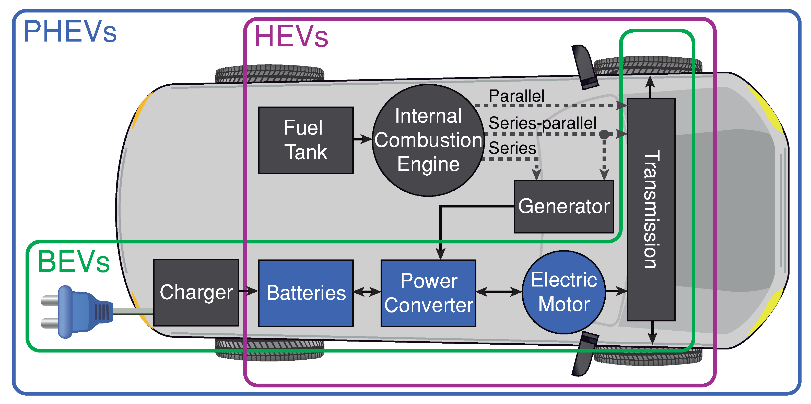
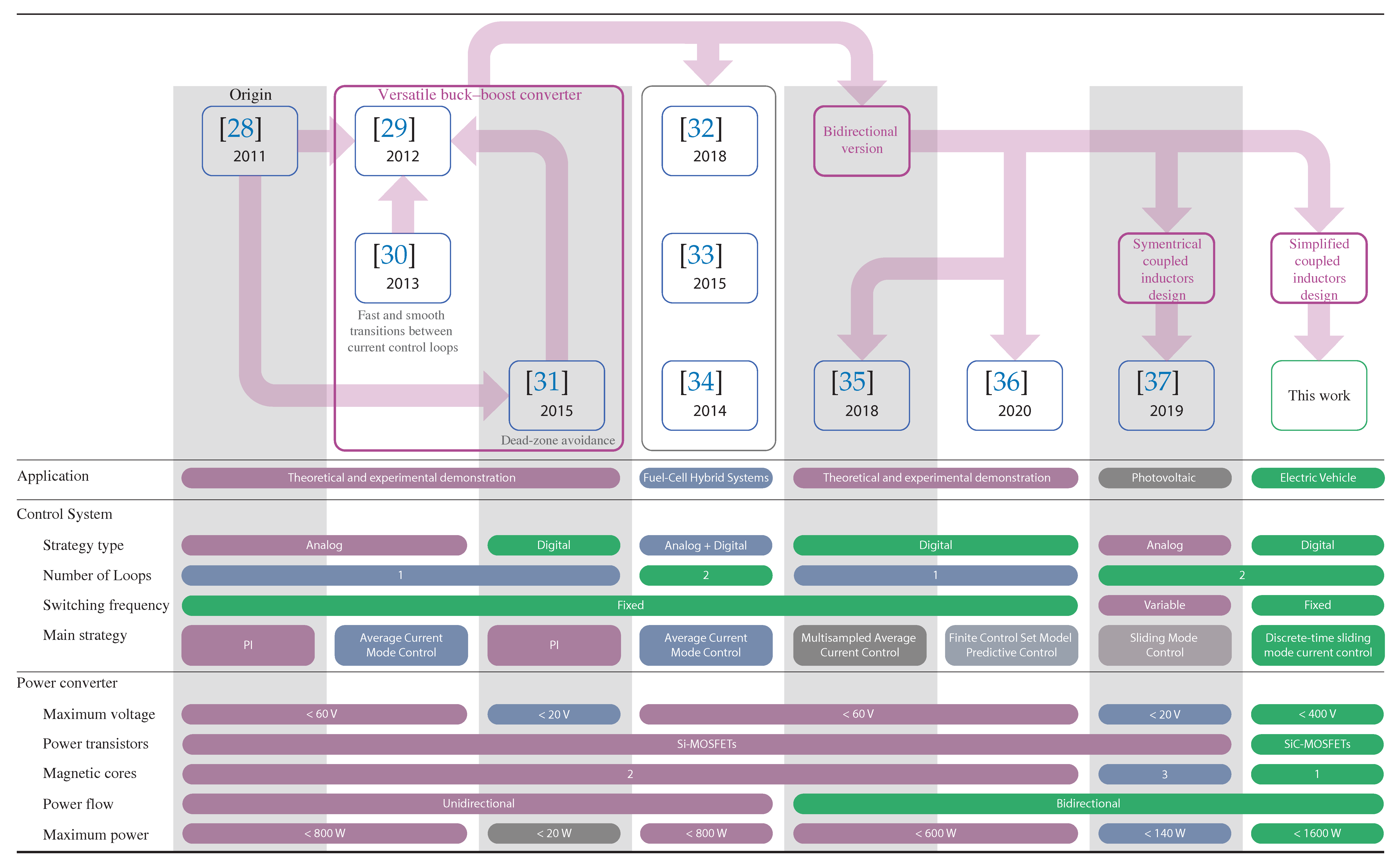
:1. Introduction
- A novel high-voltage high-switching bidirectional converter is presented. This new converter has step-up and step-down characteristics in both current directions to extend the EV traction inverter efficiency under a wide range of speeds. This converter guarantees a high power conversion efficiency for EV powertrain applications due to silicon carbide (SiC) devices and the design with a low winding-to-winding parasitic capacitance of the coupled inductor. It can operate in boost or buck mode.
- A two-loop digital control design with a current (inner loop) controller and a voltage (outer loop) controller regulate the DC-bus voltage during traction and regenerative modes. The proposed controller ensures zero steady-state voltage error and fast transient responses to the voltage reference and power variations.
- A DSMCC control is proposed for the inner loop of the voltage feedback outer loop. The proposed controller ensures fast-tracking of the control set-points and low steady-state error under demanding tests that include system start-up and dc bus voltage reference with small and large variations. It is the first time that the DSMCC control strategy is used for the versatile buck–boost converter.
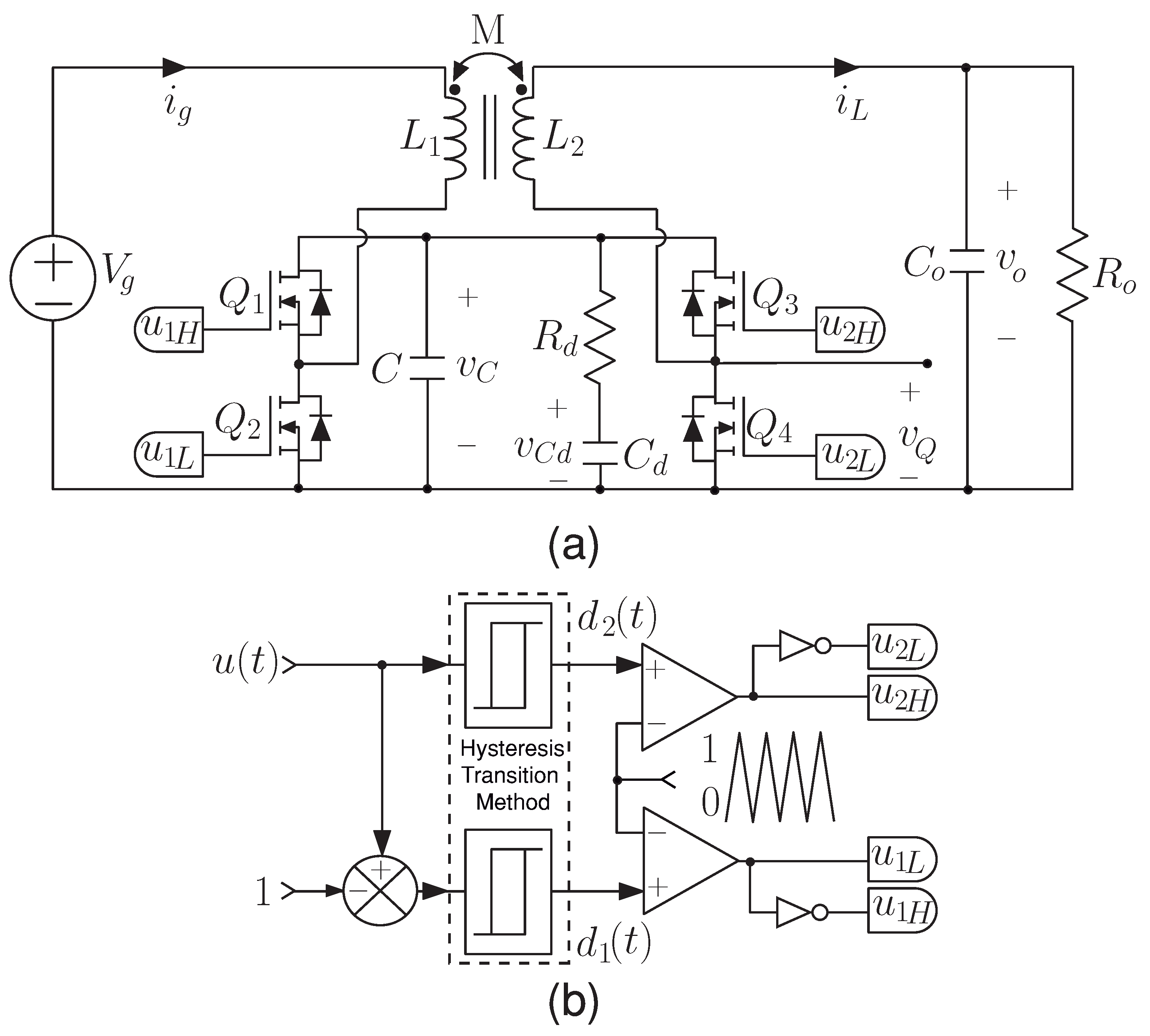
2. Bidirectional Noninverting Coupled-Inductor Buck–Boost Converter
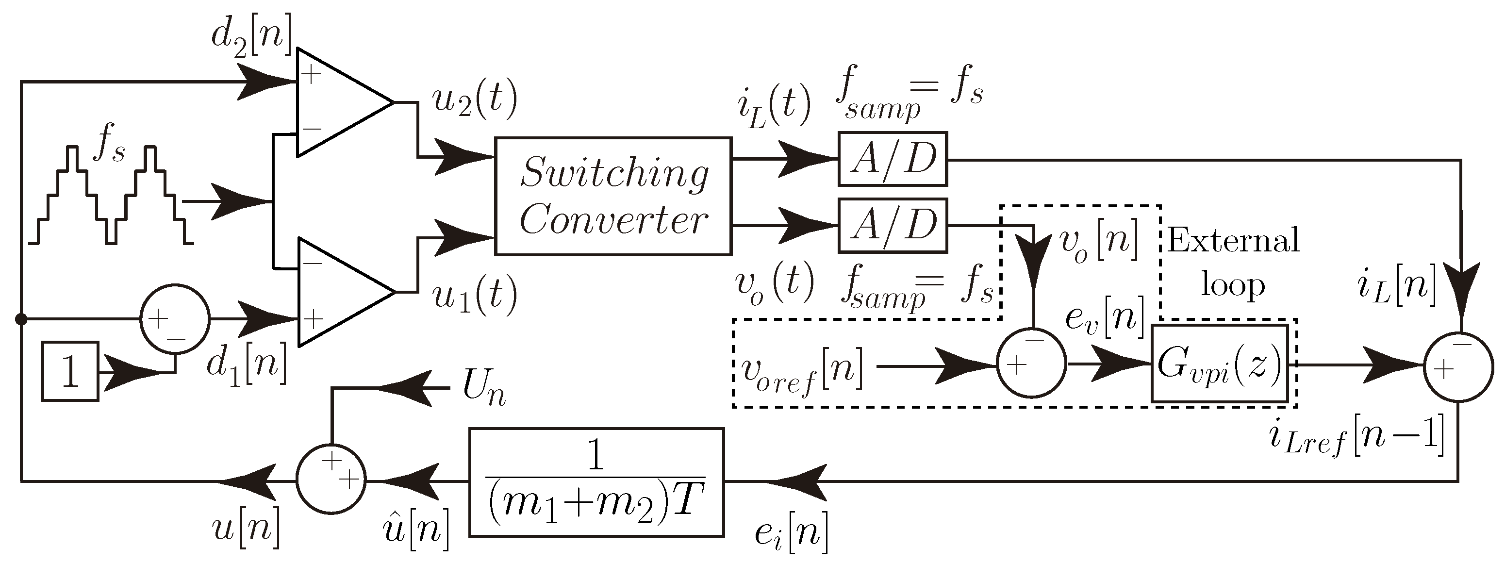
3. Digital Control for Output Voltage Regulation
3.1. Discrete-Time Sliding-Mode Current Control
3.2. Digital Proportional-Integral Voltage Control
4. Simulation and Experimental Results
4.1. System Startup
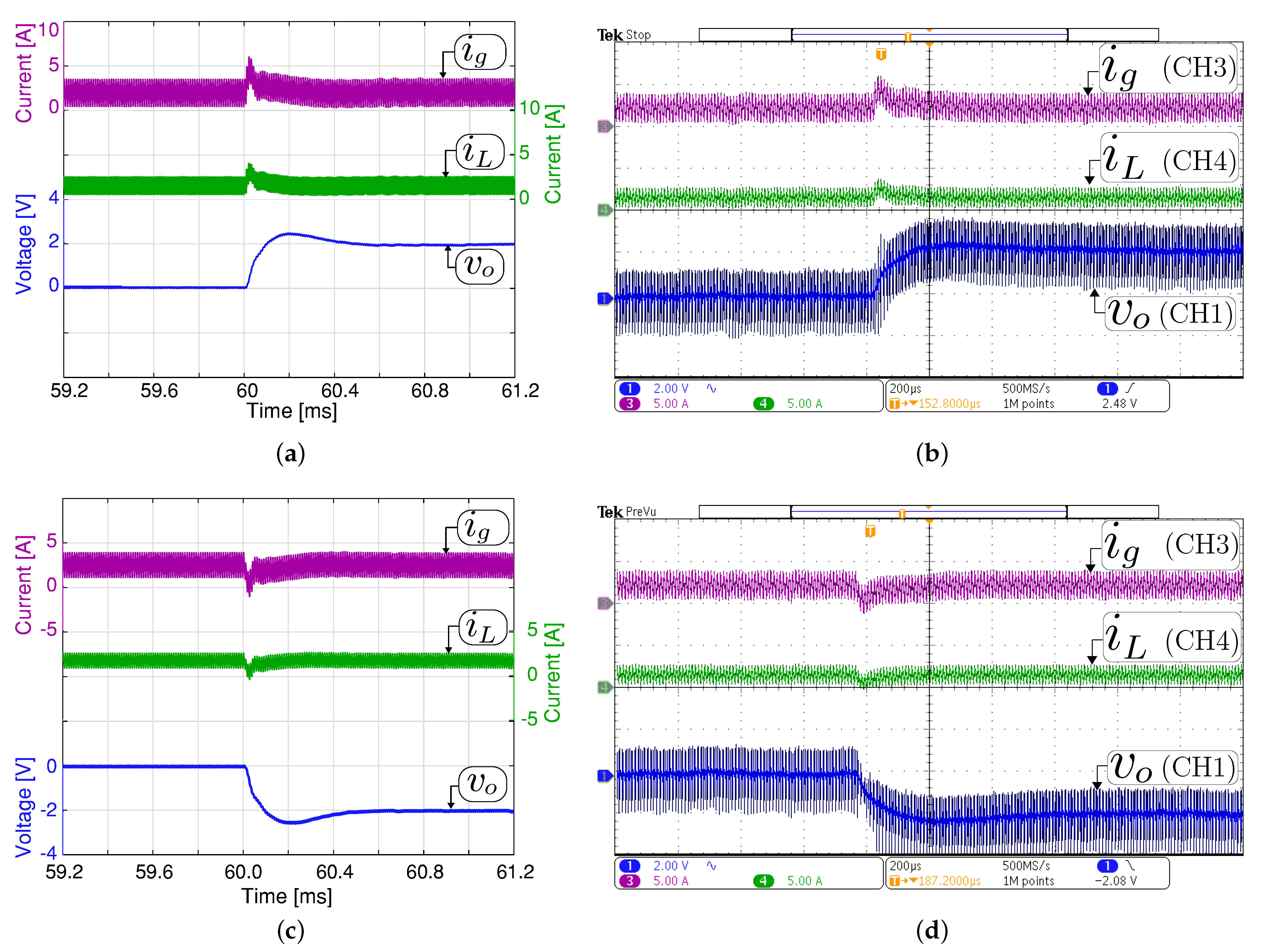
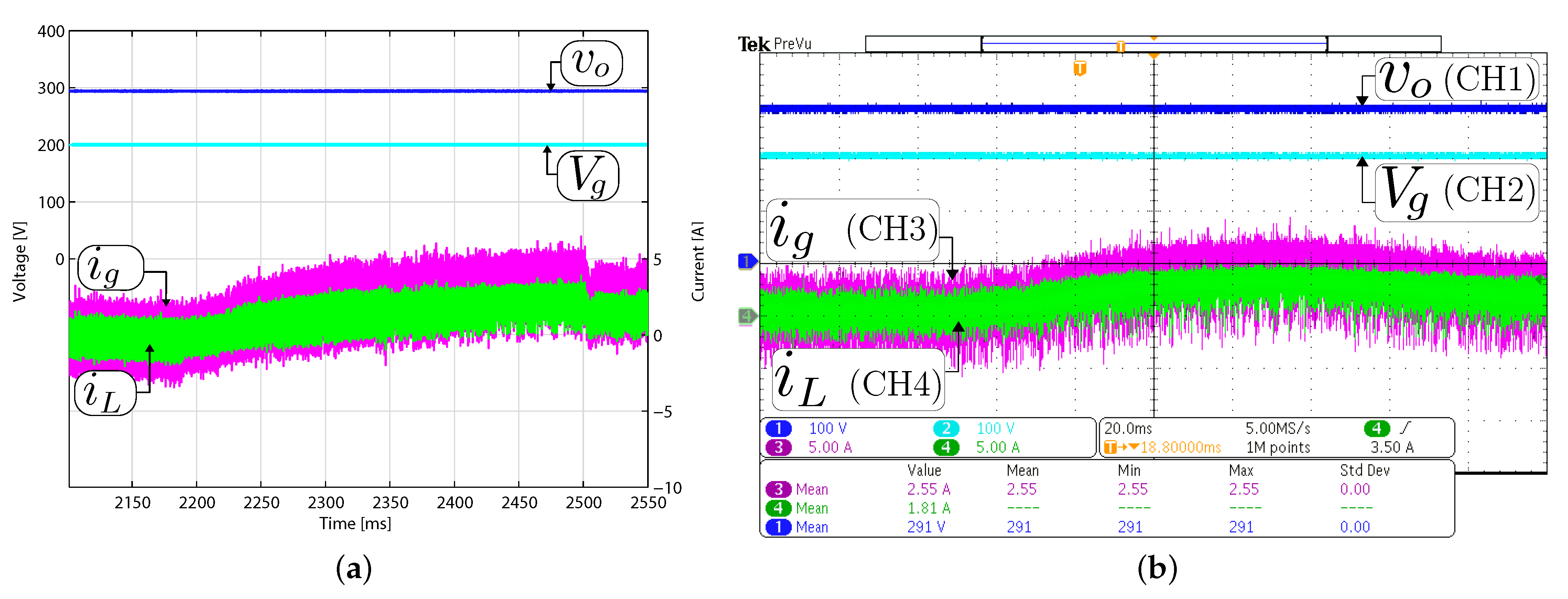
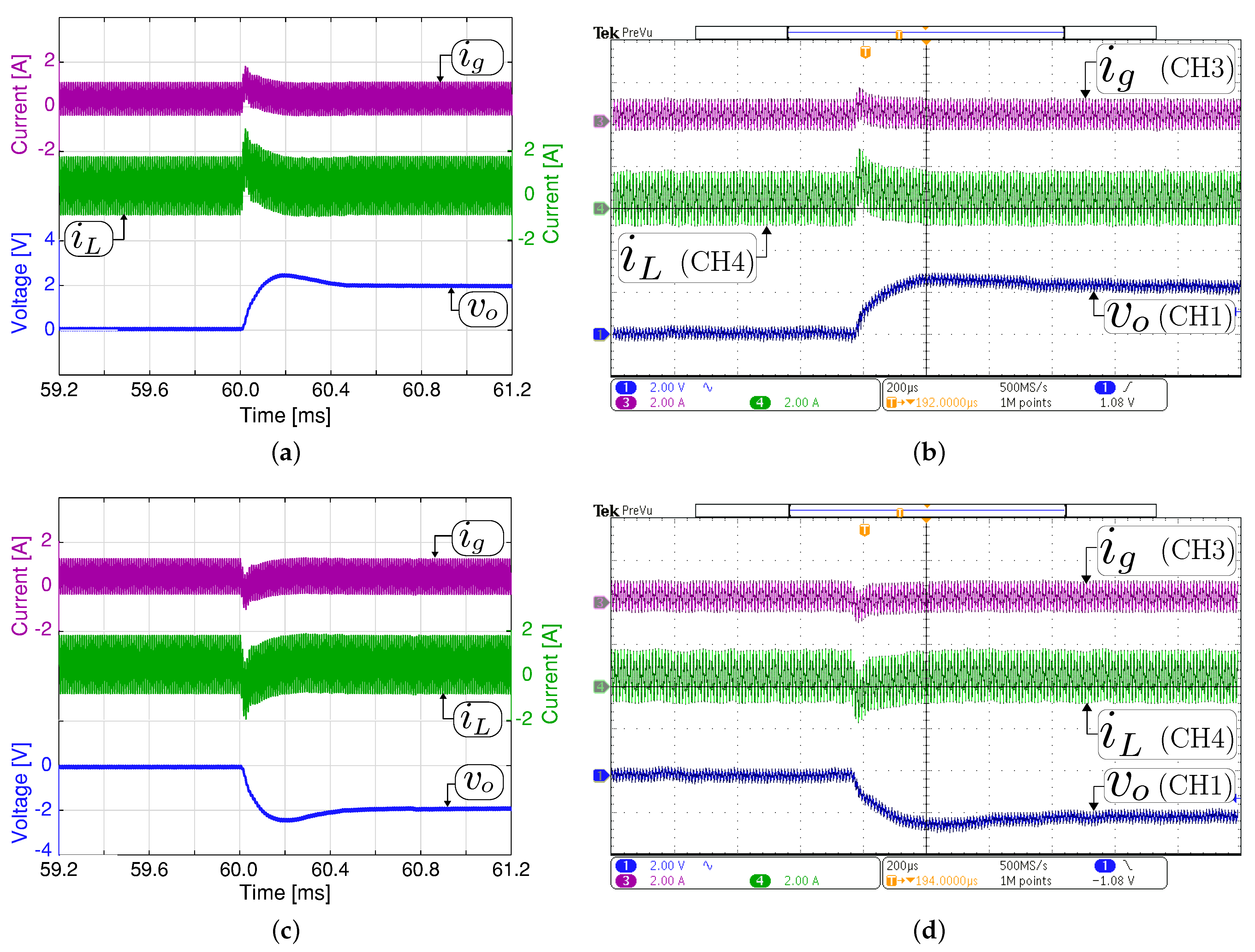
4.2. Small-Signal Response to Output Voltage Reference Variation
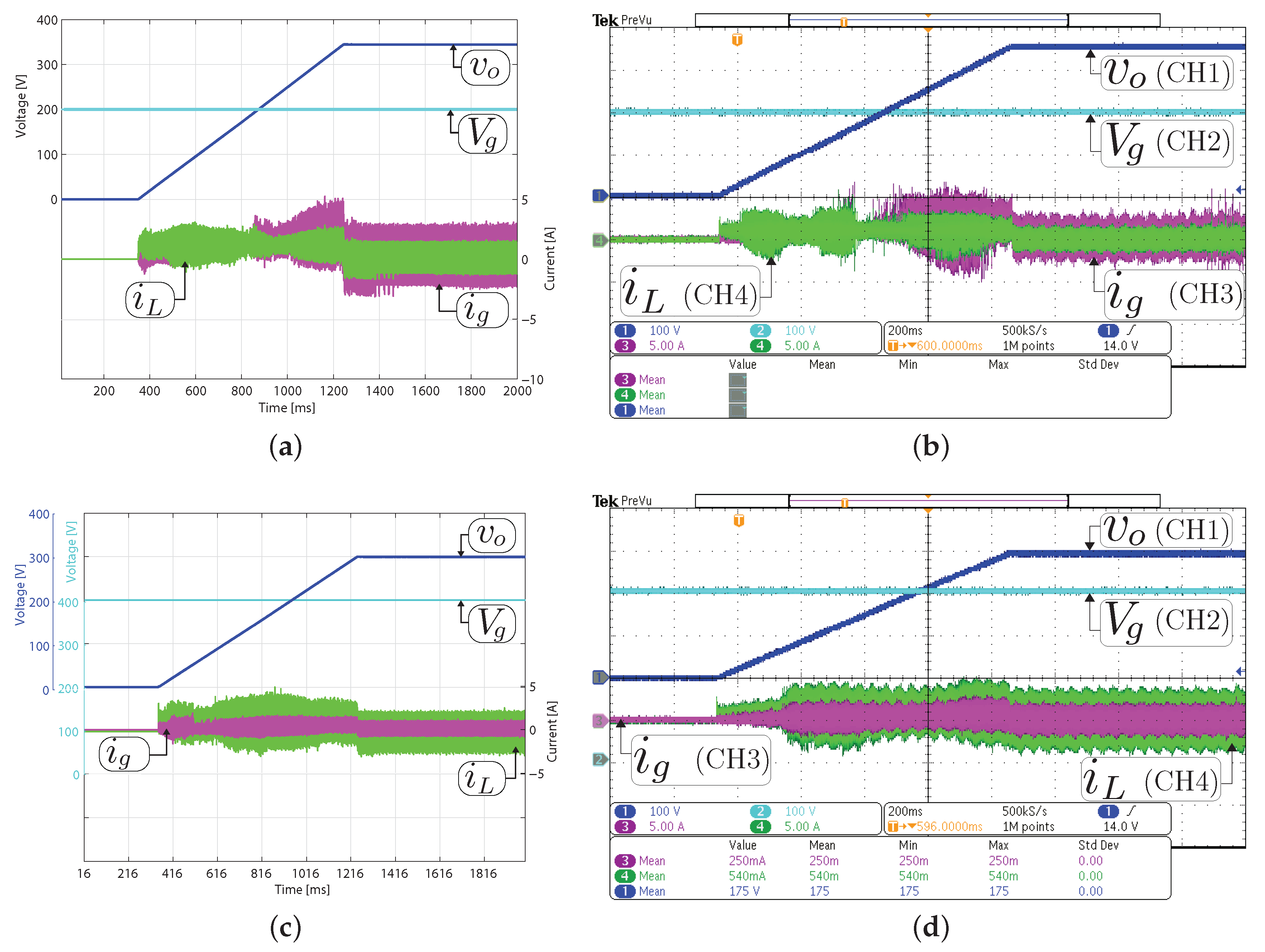
4.3. Large-Signal Response to Output Voltage Reference Variation
4.4. Experiments with an EV Powertrain System Emulation
5. Conclusions
Author Contributions
Funding
Institutional Review Board Statement
Informed Consent Statement
Data Availability Statement
Conflicts of Interest
References
- Yong, J.Y.; Ramachandaramurthy, V.K.; Tan, K.M.; Mithulananthan, N. A review on the state-of-the-art technologies of electric vehicle, its impacts and prospects. Renew. Sustain. Energy Rev. 2015, 49, 365–385. [Google Scholar] [CrossRef]
- Shi, X.; Pan, J.; Wang, H.; Cai, H. Battery electric vehicles: What is the minimum range required? Energy 2019, 166, 352–358. [Google Scholar] [CrossRef]
- Andwari, A.M.; Pesiridis, A.; Rajoo, S.; Martinez-Botas, R.; Esfahanian, V. A review of Battery Electric Vehicle technology and readiness levels. Renew. Sustain. Energy Rev. 2017, 78, 414–430. [Google Scholar] [CrossRef]
- Sewergin, A.; Wienhausen, A.H.; Oberdieck, K.; Doncker, R.W.D. Modular bidirectional full-SiC DC-DC converter for automotive applications. In Proceedings of the 2017 IEEE 12th International Conference on Power Electronics and Drive Systems (PEDS), Honolulu, HI, USA, 12–15 December 2017; pp. 277–281. [Google Scholar]
- Rothgang, S.; Baumhöfer, T.; van Hoek, H.; Lange, T.; Doncker, R.W.D.; Sauer, D.U. Modular battery design for reliable, flexible and multi-technology energy storage systems. Appl. Energy 2015, 137, 931–937. [Google Scholar] [CrossRef]
- Quraan, M.; Tricoli, P.; D’Arco, S.; Piegari, L. Efficiency Assessment of Modular Multilevel Converters for Battery Electric Vehicles. IEEE Trans. Power Electron. 2017, 32, 2041–2051. [Google Scholar] [CrossRef]
- Zhu, Z.Q.; Howe, D. Electrical Machines and Drives for Electric, Hybrid, and Fuel Cell Vehicles. Proc. IEEE 2007, 95, 746–765. [Google Scholar] [CrossRef]
- Yang, Z.; Shang, F.; Brown, I.P.; Krishnamurthy, M. Comparative Study of Interior Permanent Magnet, Induction, and Switched Reluctance Motor Drives for EV and HEV Applications. IEEE Trans. Transp. Electrif. 2015, 1, 245–254. [Google Scholar] [CrossRef]
- Song, Z.; Liu, C.; Zhao, H. Investigation on Magnetic Force of a Flux-Modulated Double-Rotor Permanent Magnet Synchronous Machine for Hybrid Electric Vehicle. IEEE Trans. Transp. Electrif. 2019, 5, 1383–1394. [Google Scholar] [CrossRef]
- Cheng, M.; Sun, L.; Buja, G.; Song, L. Advanced Electrical Machines and Machine-Based Systems for Electric and Hybrid Vehicles. Energies 2015, 8, 9541–9564. [Google Scholar] [CrossRef] [Green Version]
- Zhao, N.; Schofield, N.; Yang, R.; Gu, R. Investigation of DC-Link voltage and temperature variations on EV traction system design. IEEE Trans. Ind. Appl. 2017, 53, 3707–3718. [Google Scholar] [CrossRef]
- Lin, Y.S.; Hu, K.W.; Yeh, T.H.; Liaw, C.M. An electric-vehicle IPMSM drive with interleaved front-end DC/DC converter. IEEE Trans. Veh. Technol. 2015, 65, 4493–4504. [Google Scholar] [CrossRef]
- Deng, W.; Zhao, Y.; Wu, J. Energy efficiency improvement via bus voltage control of inverter for electric vehicles. IEEE Trans. Veh. Technol. 2016, 66, 1063–1073. [Google Scholar] [CrossRef]
- Chen, H.; Kim, H.; Erickson, R.; Maksimović, D. Electrified Automotive Powertrain Architecture Using Composite DC–DC Converters. IEEE Trans. Power Electron. 2017, 32, 98–116. [Google Scholar] [CrossRef]
- Qian, W.; Cha, H.; Peng, F.Z.; Tolbert, L.M. 55-kW variable 3X DC-DC converter for plug-in hybrid electric vehicles. IEEE Trans. Power Electron. 2012, 27, 1668–1678. [Google Scholar] [CrossRef]
- Elsayad, N.; Moradisizkoohi, H.; Mohammed, O.A. A New Hybrid Structure of a Bidirectional DC-DC Converter With High Conversion Ratios for Electric Vehicles. IEEE Trans. Veh. Technol. 2019, 69, 194–206. [Google Scholar] [CrossRef]
- Reimers, J.; Dorn-Gomba, L.; Mak, C.; Emadi, A. Automotive traction inverters: Current status and future trends. IEEE Trans. Veh. Technol. 2019, 68, 3337–3350. [Google Scholar] [CrossRef]
- Dusmez, S.; Hasanzadeh, A.; Khaligh, A. Comparative analysis of bidirectional three-level DC–DC converter for automotive applications. IEEE Trans. Ind. Electron. 2015, 62, 3305–3315. [Google Scholar] [CrossRef]
- Pavlovskỳ, M.; Guidi, G.; Kawamura, A. Assessment of coupled and independent phase designs of interleaved multiphase buck/boost DC–DC converter for EV power train. IEEE Trans. Power Electron. 2013, 29, 2693–2704. [Google Scholar] [CrossRef]
- Lu, X.; Wang, H. A highly efficient multifunctional power electronic interface for PEV hybrid energy management systems. IEEE Access 2018, 7, 8964–8974. [Google Scholar] [CrossRef]
- Hegazy, O.; Mierlo, J.V.; Lataire, P. Analysis, Modeling, and Implementation of a Multidevice Interleaved DC/DC Converter for Fuel Cell Hybrid Electric Vehicles. IEEE Trans. Power Electron. 2012, 27, 4445–4458. [Google Scholar] [CrossRef]
- Onar, O.C.; Kobayashi, J.; Erb, D.C.; Khaligh, A. A Bidirectional High-Power-Quality Grid Interface With a Novel Bidirectional Noninverted Buck–Boost Converter for PHEVs. IEEE Trans. Veh. Technol. 2012, 61, 2018–2032. [Google Scholar] [CrossRef]
- Han, D.; Noppakunkajorn, J.; Sarlioglu, B. Comprehensive efficiency, weight, and volume comparison of SiC-and Si-based bidirectional DC–DC converters for hybrid electric vehicles. IEEE Trans. Veh. Technol. 2014, 63, 3001–3010. [Google Scholar] [CrossRef]
- Lai, C.M.; Cheng, Y.H.; Hsieh, M.H.; Lin, Y.C. Development of a Bidirectional DC/DC Converter With Dual-Battery Energy Storage for Hybrid Electric Vehicle System. IEEE Trans. Veh. Technol. 2018, 67, 1036–1052. [Google Scholar] [CrossRef]
- Guo, J.; Rodriguez, R.; Gareau, J.; Schumacher, D.; Alizadeh, M.; Azer, P.; Bauman, J.; Bilgin, B.; Emadi, A. A Comprehensive Analysis for High-Power Density, High-Efficiency 60 kW Interleaved Boost Converter Design for Electrified Powertrains. IEEE Trans. Veh. Technol. 2020, 69, 7131–7145. [Google Scholar] [CrossRef]
- Sun, Q.; Wu, J.; Gan, C.; Si, J.; Guo, J.; Hu, Y. Cascaded Multiport Converter for SRM-Based Hybrid Electrical Vehicle Applications. IEEE Trans. Power Electron. 2019, 34, 11940–11951. [Google Scholar] [CrossRef]
- Estima, J.O.; Cardoso, A.J.M. Efficiency Analysis of Drive Train Topologies Applied to Electric/Hybrid Vehicles. IEEE Trans. Veh. Technol. 2012, 61, 1021–1031. [Google Scholar] [CrossRef]
- Restrepo, C.; Calvente, J.; Cid-Pastor, A.; El Aroudi, A.; Giral, R. A noninverting buck–boost DC–DC switching converter with high efficiency and wide bandwidth. IEEE Trans. Power Electron. 2011, 26, 2490–2503. [Google Scholar] [CrossRef]
- Restrepo, C.; Calvente, J.; Romero, A.; Vidal-Idiarte, E.; Giral, R. Current-Mode Control of a Coupled-Inductor Buck–Boost DC–DC Switching Converter. IEEE Trans. Power Electron. 2012, 27, 2536–2549. [Google Scholar] [CrossRef]
- Restrepo, C.; Konjedic, T.; Calvente, J.; Milanovic, M.; Giral, R. Fast Transitions Between Current Control Loops of the Coupled-Inductor Buck–Boost DC–DC Switching Converter. IEEE Trans. Power Electron. 2013, 28, 3648–3652. [Google Scholar] [CrossRef]
- Restrepo, C.; Konjedic, T.; Calvente, J.; Giral, R. Hysteretic transition method for avoiding the dead-zone effect and subharmonics in a noninverting buck–boost converter. IEEE Trans. Power Electron. 2015, 30, 3418–3430. [Google Scholar] [CrossRef] [Green Version]
- Ramírez-Murillo, H.; Restrepo, C.; Konjedic, T.; Calvente, J.; Romero, A.; Baier, C.R.; Giral, R. An Efficiency Comparison of Fuel-Cell Hybrid Systems Based on the Versatile Buck–Boost Converter. IEEE Trans. Power Electron. 2018, 33, 1237–1246. [Google Scholar] [CrossRef]
- Ramírez-Murillo, H.; Restrepo, C.; Calvente, J.; Romero, A.; Giral, R. Energy Management of a Fuel-Cell Serial–Parallel Hybrid System. IEEE Trans. Ind. Electron. 2015, 62, 5227–5235. [Google Scholar] [CrossRef]
- Ramírez-Murillo, H.; Restrepo, C.; Calvente, J.; Romero, A.; Giral, R. Energy Management DC System Based on Current-Controlled Buck-Boost Modules. IEEE Trans. Smart Grid 2014, 5, 2644–2653. [Google Scholar] [CrossRef]
- Restrepo, C.; Konjedic, T.; Flores-Bahamonde, F.; Vidal-Idiarte, E.; Calvente, J.; Giral, R. Multisampled Digital Average Current Controls of the Versatile Buck-Boost Converter. IEEE J. Emerg. Sel. Top. Power Electron. 2018, 7, 879–890. [Google Scholar] [CrossRef]
- Restrepo, C.; Garcia, G.; Flores-Bahamonde, F.; Murillo-Yarce, D.; Guzman, J.I.; Rivera, M. Current Control of the Coupled-Inductor Buck–Boost DC–DC Switching Converter using a Model Predictive Control Approach. IEEE J. Emerg. Sel. Top. Power Electron. 2020, 8, 3348–3360. [Google Scholar] [CrossRef]
- Méndez-Díaz, F.; Pico, B.; Vidal-Idiarte, E.; Calvente, J.; Giral, R. HM/PWM Seamless Control of a Bidirectional Buck–Boost Converter for a Photovoltaic Application. IEEE Trans. Power Electron. 2019, 34, 2887–2899. [Google Scholar] [CrossRef]
- Zhang, L.; Yuan, X.; Wu, X.; Shi, C.; Zhang, J.; Zhang, Y. Performance evaluation of high-power SiC MOSFET modules in comparison to Si IGBT modules. IEEE Trans. Power Electron. 2018, 34, 1181–1196. [Google Scholar] [CrossRef]
- Bosshard, R.; Kolar, J.W. All-SiC 9.5 kW/dm3 on-board power electronics for 50 kW/85 kHz automotive IPT system. IEEE J. Emerg. Sel. Top. Power Electron. 2016, 5, 419–431. [Google Scholar] [CrossRef]
- Ghazanfari, A.; Perreault, C.; Zaghib, K. EV/HEV Industry Trends of Wide-bandgap Power Semiconductor Devices for Power Electronics Converters. In Proceedings of the 2019 IEEE 28th International Symposium on Industrial Electronics (ISIE), Vancouver, BC, Canada, 12–14 June 2019; pp. 1917–1923. [Google Scholar]
- González-Castaño, C.; Restrepo, C.; Giral, R.; García-Amoros, J.; Vidal-Idiarte, E.; Calvente, J. Coupled inductors design of the bidirectional non-inverting buck–boost converter for high-voltage applications. IET Power Electron. 2020, 13, 3188–3198. [Google Scholar] [CrossRef]
- Kim, B.S.; Kim, H.J.; Jin, C.; Huh, D.Y. A digital controlled DC-DC converter for electric vehicle applications. In Proceedings of the 2011 International Conference on Electrical Machines and Systems (ICEMS), Beijing, China, 20–23 August 2011; pp. 1–5. [Google Scholar]
- Vidal-Idiarte, E.; Marcos-Pastor, A.; Garcia, G.; Cid-Pastor, A.; Martinez-Salamero, L. Discrete-time sliding-mode-based digital pulse width modulation control of a boost converter. IET Power Electron. 2015, 8, 708–714. [Google Scholar] [CrossRef]
- Vidal-Idiarte, E.; Marcos-Pastor, A.; Giral, R.; Calvente, J.; Martinez-Salamero, L. Direct digital design of a sliding mode-based control of a PWM synchronous buck converter. IET Power Electron. 2017, 10, 1714–1720. [Google Scholar] [CrossRef]
- Teodorescu, R.; Liserre, M.; Rodriguez, P. Grid Converters for Photovoltaic and Wind Power Systems; John Wiley & Sons: New York, NY, USA, 2011; Volume 29. [Google Scholar]
- Geng, Z.; Hong, T.; Qi, K.; Ambrosio, J.; Gu, D. Modular Regenerative Emulation System for DC–DC Converters in Hybrid Fuel Cell Vehicle Applications. IEEE Trans. Veh. Technol. 2018, 67, 9233–9240. [Google Scholar] [CrossRef]


| Mode | ||
|---|---|---|
| Buck | ||
| Boost |
| Mode | Simulated | Experimental | ||
|---|---|---|---|---|
| CF | PM | CF | PM | |
| [kHz] | [deg] | [kHz] | [deg] | |
| Boost | 1.99 | 63.79 | 2.03 | 79.4 |
| Buck | 1.99 | 66.52 | 1.94 | 71.2 |
| Parameter | Value or Type |
|---|---|
| Input voltage | 200–400 V |
| Output voltage | 100–400 V |
| Rated Power | 1.6 kW |
| Switching frequency | 100 kHz |
| Output capacitor | 6× R75PW44704030J, 28 F, 630 V |
| Damping capacitor | MKP1848S62070JP2F, 20 F, 700 V |
| Intermediate capacitor C | 4× R76PN33304030J, 1.32 F, 630 V |
| Coupled inductor | 135 H and 270 H, |
| Core: 77,908 Magnetics, | |
| Number turns: 80, | |
| Wire size: 18 AWG. | |
| Damping resistance | 2× BPR10100J in parallel, 5 , |
| 10 W, 500 V | |
| MOSFET Driver | UCC27714D |
| Power semiconductors | SCT2450KEC |
| Parameter | 90 SL | 100 L |
|---|---|---|
| Motor rated speed | 1500 [rpm] | 1500 [rpm] |
| Number of pole pairs | 8 | 8 |
| Stator resistance | 2.34 | 1.277 |
| d-axis inductance | 50.124 mH | 29.128 mH |
| q-axis inductance | 29.128 mH | 19.295 mH |
| Moment of inertia J | 0.0032 kg·m | 0.0066 kg·m |
| Electrical constant | 212 | 223 |
Publisher’s Note: MDPI stays neutral with regard to jurisdictional claims in published maps and institutional affiliations. |
© 2021 by the authors. Licensee MDPI, Basel, Switzerland. This article is an open access article distributed under the terms and conditions of the Creative Commons Attribution (CC BY) license (https://creativecommons.org/licenses/by/4.0/).
Share and Cite
González-Castaño, C.; Restrepo, C.; Kouro, S.; Vidal-Idiarte, E.; Calvente, J. A Bidirectional Versatile Buck–Boost Converter Driver for Electric Vehicle Applications. Sensors 2021, 21, 5712. https://doi.org/10.3390/s21175712
González-Castaño C, Restrepo C, Kouro S, Vidal-Idiarte E, Calvente J. A Bidirectional Versatile Buck–Boost Converter Driver for Electric Vehicle Applications. Sensors. 2021; 21(17):5712. https://doi.org/10.3390/s21175712
Chicago/Turabian StyleGonzález-Castaño, Catalina, Carlos Restrepo, Samir Kouro, Enric Vidal-Idiarte, and Javier Calvente. 2021. "A Bidirectional Versatile Buck–Boost Converter Driver for Electric Vehicle Applications" Sensors 21, no. 17: 5712. https://doi.org/10.3390/s21175712
APA StyleGonzález-Castaño, C., Restrepo, C., Kouro, S., Vidal-Idiarte, E., & Calvente, J. (2021). A Bidirectional Versatile Buck–Boost Converter Driver for Electric Vehicle Applications. Sensors, 21(17), 5712. https://doi.org/10.3390/s21175712