Design of an Ultrasound Transceiver ASIC with a Switching-Artifact Reduction Technique for 3D Carotid Artery Imaging

 , , , , , and
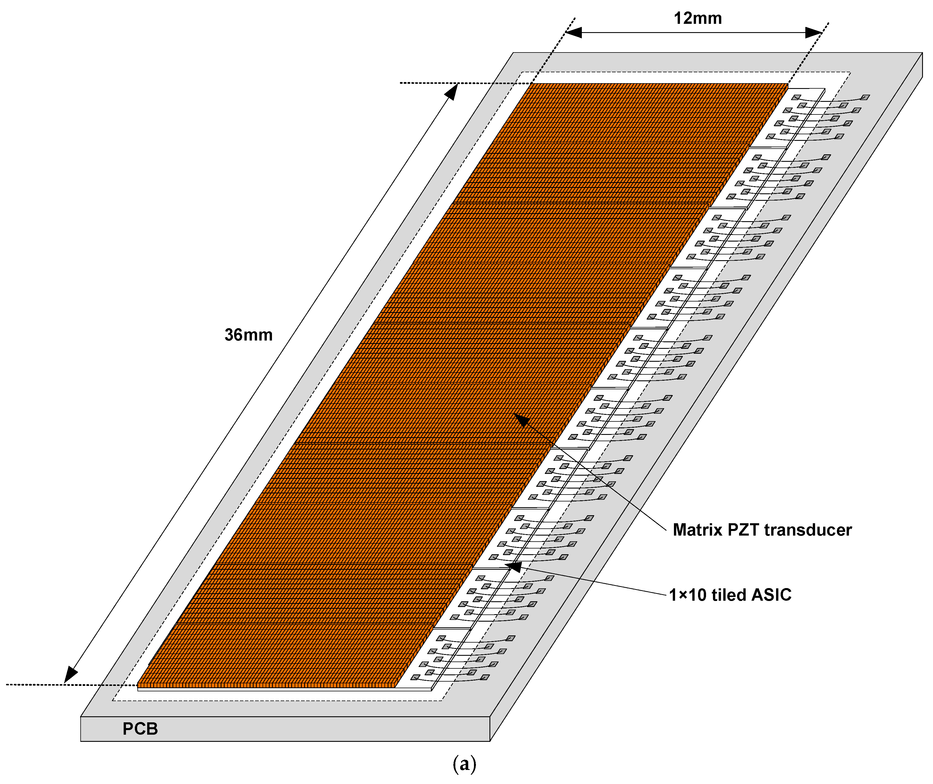
Abstract
1. Introduction
2. Materials and Methods
2.1. System Overview
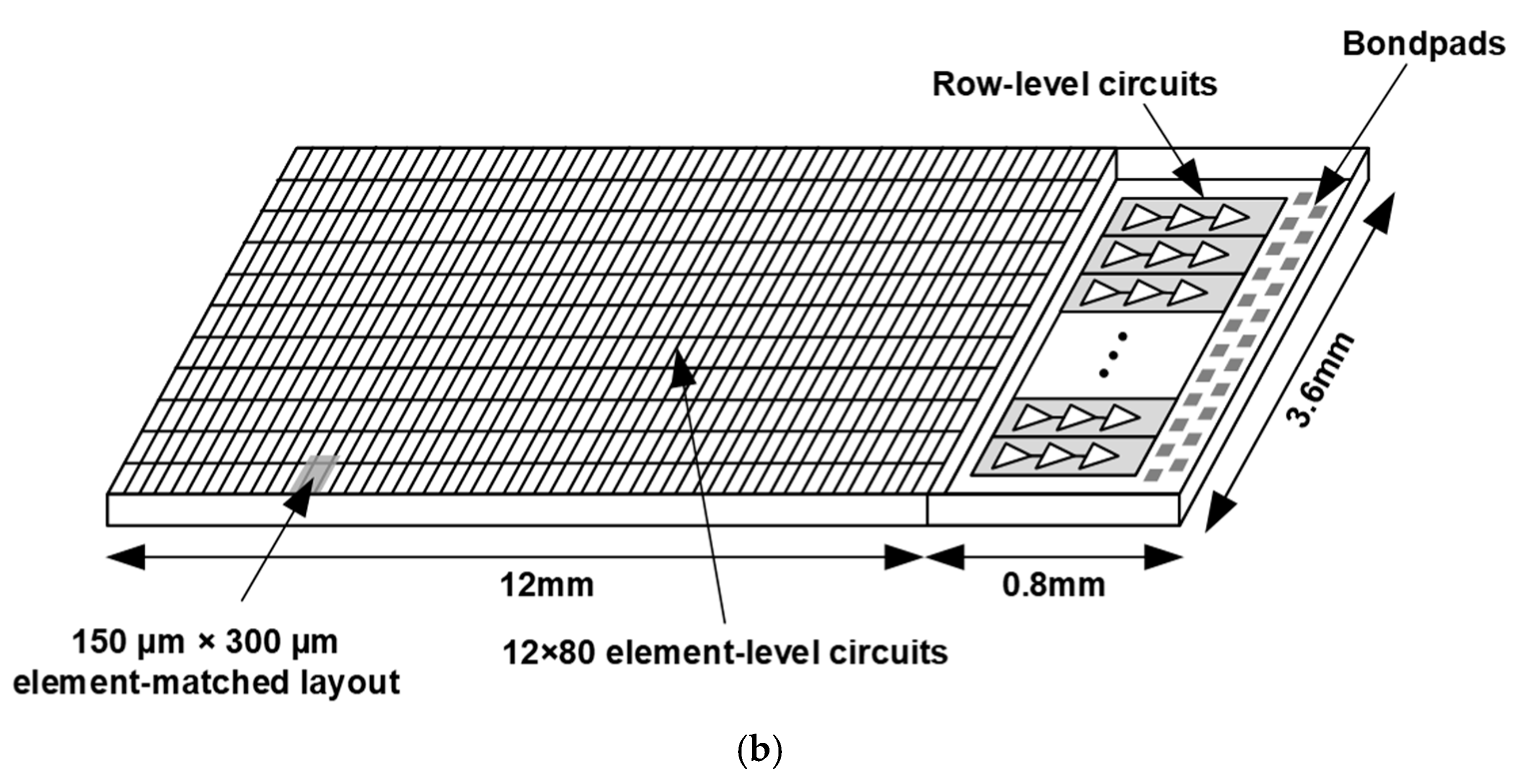
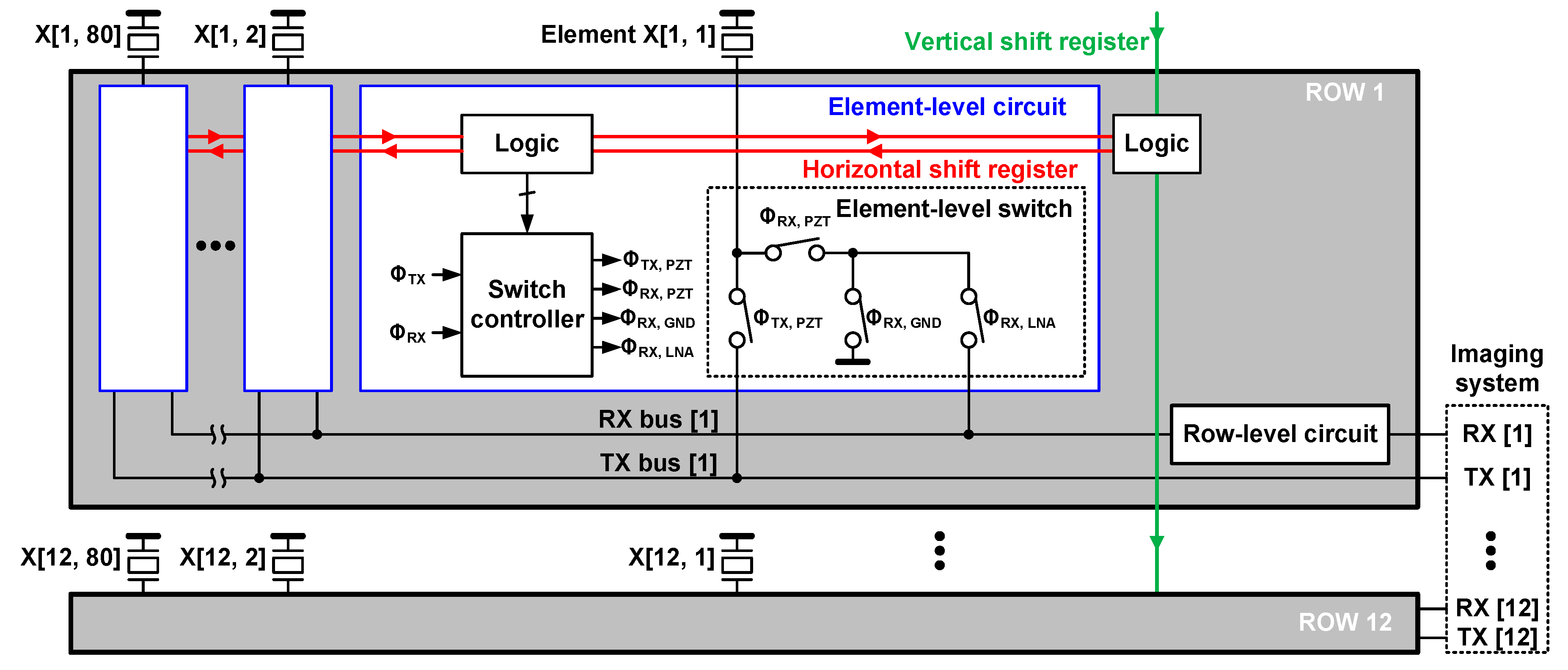
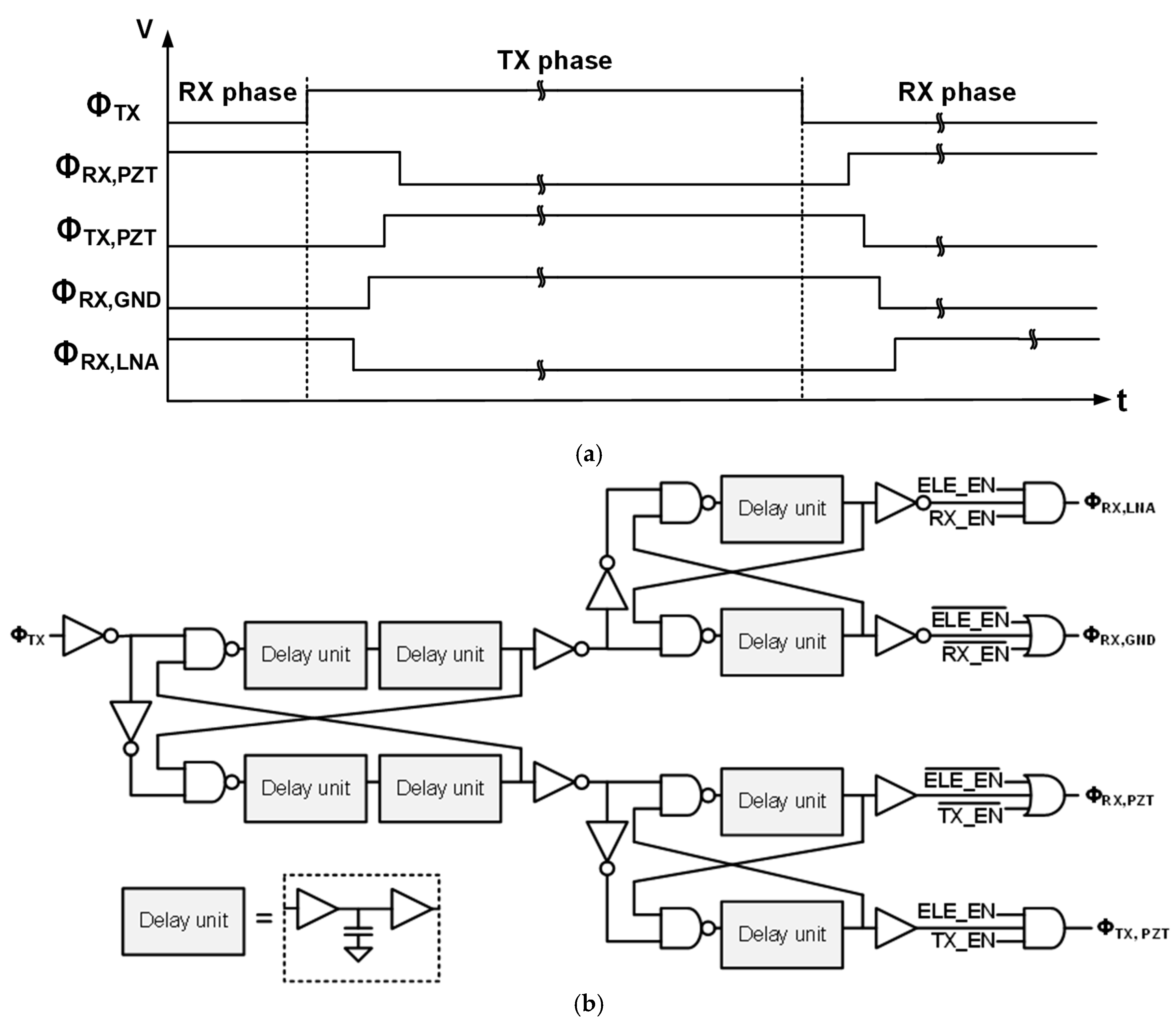
2.2. ASIC Architecture
2.3. Element-Level Switch Circuit and Non-Idealities
2.4. Proposed Switch Controller
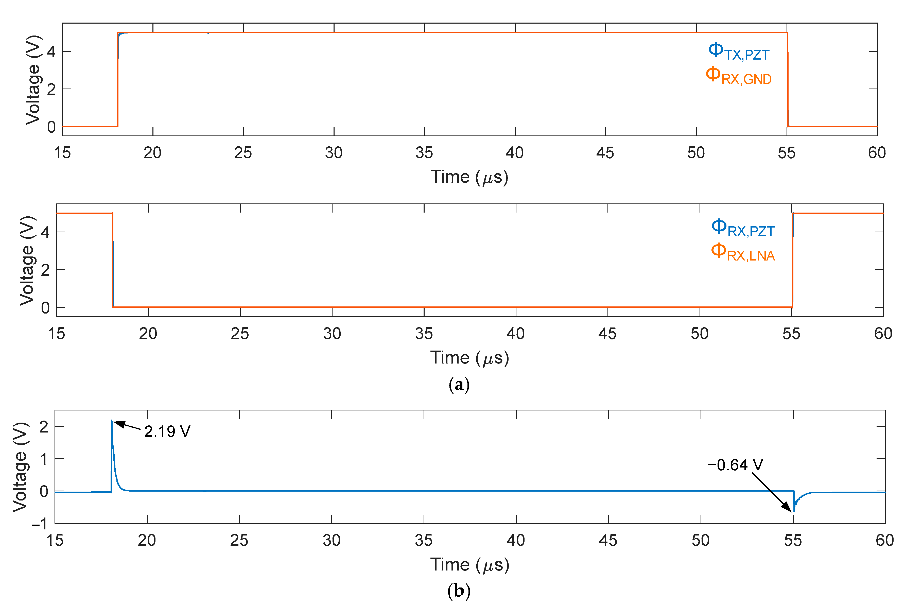
2.5. Validation in Simulation
3. Results and Discussion
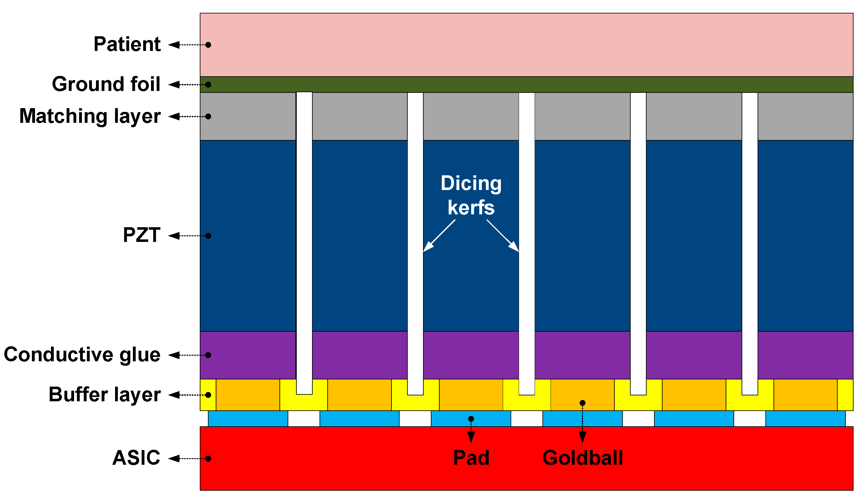
3.1. Experimental Prototype
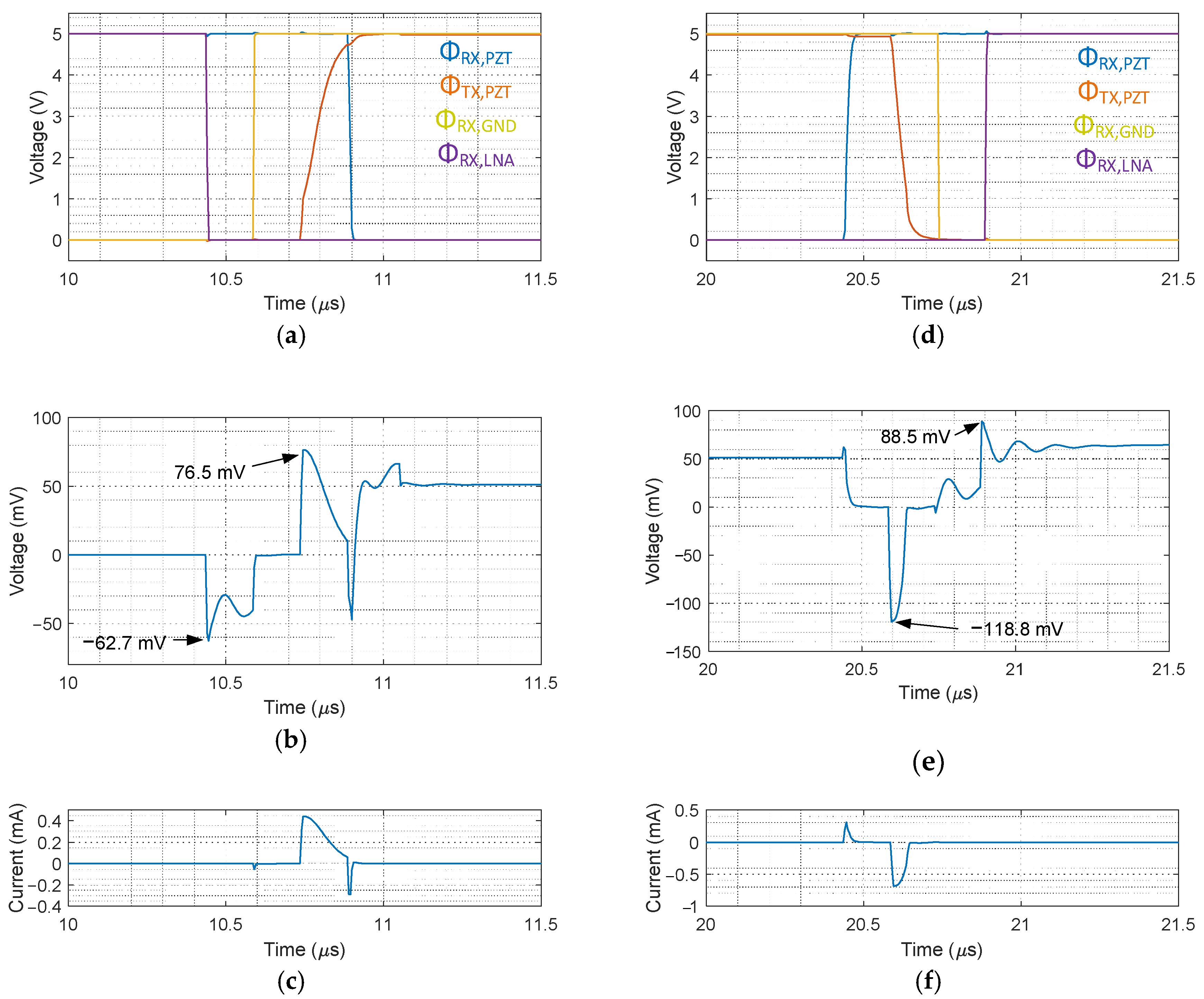
3.2. Electrical Verification
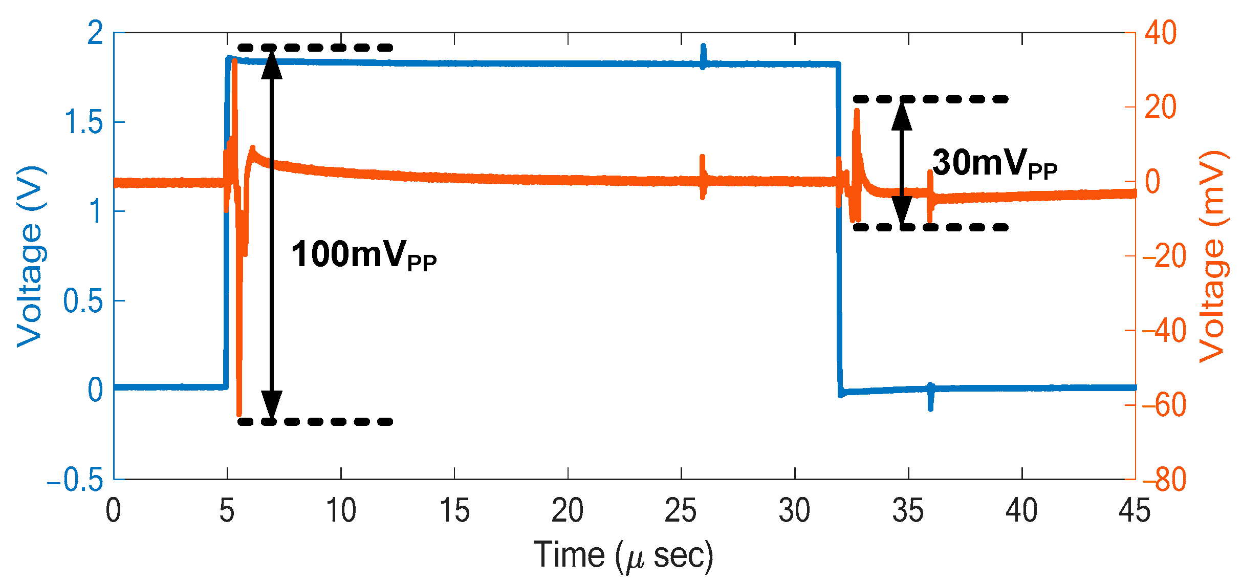
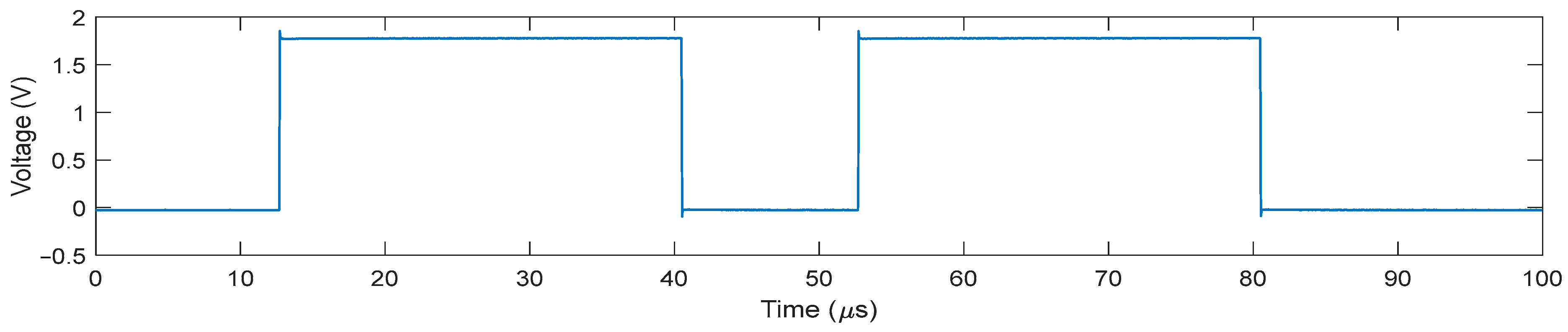
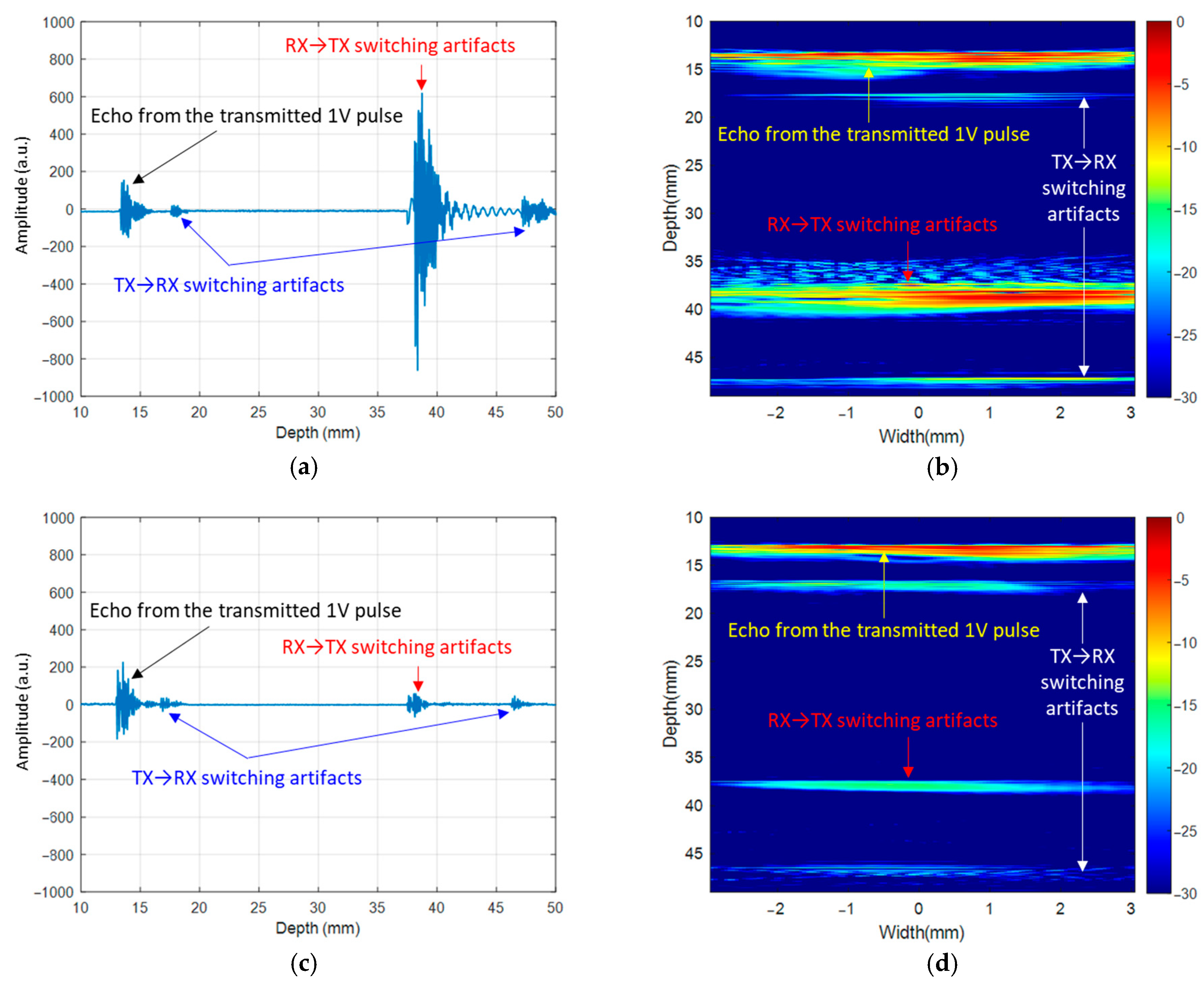
3.3. Improvement in Clock Feedthrough and Charge Injection-Induced Imaging Artifact
4. Conclusions
Author Contributions
Funding
Informed Consent Statement
Data Availability Statement
Conflicts of Interest
References
- Couade, M.; Pernot, M.; Messas, E.; Emmerich, J.; Hagège, A.; Fink, M.; Tanter, M. Ultrafast imaging of the arterial pulse wave. IRBM 2011, 32, 106–108. [Google Scholar] [CrossRef]
- Hasegawa, H.; Hongo, K.; Kanai, H. Measurement of regional pulse wave velocity using very high frame rate ultrasound. J. Med. Ultrason. 2012, 40, 91–98. [Google Scholar] [CrossRef] [PubMed]
- Kruizinga, P.; Mastik, F.; Oord, S.C.V.D.; Schinkel, A.F.L.; Bosch, J.G.; De Jong, N.; Van Soest, G.; Van Der Steen, A.F. High-definition imaging of carotid artery wall dynamics. Ultrasound Med. Biol. 2014, 40, 2392–2403. [Google Scholar] [CrossRef] [PubMed]
- Provost, J.; Papadacci, C.; Arango, J.E.; Imbault, M.; Fink, M.; Gennisson, J.-L.; Anter, M.; Pernot, M. 3D ultrafast ultrasound imaging in vivo. Phys. Med. Biol. 2014, 59, 1–13. [Google Scholar] [CrossRef] [PubMed]
- Savord, B.; Solomon, R. Fully sampled matrix transducer for real time 3D ultrasonic imaging. In Proceedings of the IEEE Symposium on Ultrasonics, 2003, Honolulu, HI, USA, 5–8 October 2003. [Google Scholar]
- Chen, C.; Vos, H.J.; Bosch, J.G.; Hay, T.A.; De Jong, N.; Pertijs, M.A.P.; Chen, Z.; Bera, D.; Raghunathan, S.B.; Shabanimotlagh, M.; et al. A front-end ASIC with receive sub-array beamforming integrated with a 32 × 32 PZT matrix transducer for 3-D transesophageal echocardiography. IEEE J. Solid-State Circuits 2017, 52, 994–1006. [Google Scholar] [CrossRef]
- Kim, T.; Shin, S.; Kim, S. An 80.2 dB DR 23.25 mW/channel 8-channel ultrasound receiver with a beamforming embedded SAR ADC. IEEE Trans. Circuits Syst. II Express Briefs 2018, 66, 1487–1491. [Google Scholar] [CrossRef]
- Igarashi, Y.; Kajiyama, S.; Katsube, Y.; Nishimoto, T.; Nakagawa, T.; Okuma, Y.; Nakamura, Y.; Terada, T.; Yamawaki, T.; Yazaki, T.; et al. Single-chip 3072-element-channel transceiver/128-subarray-channel 2-D array IC with analog RX and all-digital TX beamformer for echocardiography. IEEE J. Solid-State Circuits 2019, 54, 2555–2567. [Google Scholar] [CrossRef]
- Wygant, I.O.; Jamal, N.S.; Lee, H.J.; Nikoozadeh, A.; Oralkan, O.; Karaman, M.; Khuri-Yakub, B.T. An integrated circuit with transmit beamforming flip-chip bonded to a 2-D CMUT array for 3-D ultrasound imaging. IEEE Trans. Ultrason. Ferroelectr. Freq. Control. 2009, 56, 2145–2156. [Google Scholar] [CrossRef] [PubMed]
- Bhuyan, A.; Choe, J.W.; Lee, B.C.; Wygant, I.O.; Nikoozadeh, A.; Oralkan, O.; Khuri-Yakub, B.T. Integrated circuits for volumetric ultrasound imaging with 2-D CMUT arrays. IEEE Trans. Biomed. Circuits Syst. 2014, 7, 796–804. [Google Scholar] [CrossRef] [PubMed]
- Chen, K.; Lee, H.-S.; Chandrakasan, A.P.; Sodini, C.G. Ultrasonic imaging transceiver design for CMUT: A three-level 30-Vpp pulse-shaping pulser with improved efficiency and a noise-optimized receiver. IEEE J. Solid-State Circuits 2013, 48, 2734–2745. [Google Scholar] [CrossRef]
- Kim, B.-H.; Kim, Y.; Lee, S.; Cho, K.; Song, J. Design and test of a fully controllable 64x128 2-D cmut array integrated with reconfigurable frontend asics for volumetric ultrasound imaging. In Proceedings of the 2012 IEEE International Ultrasonics Symposium, Dresden, Germany, 7–10 October 2012. [Google Scholar]
- Chen, K.; Lee, H.-S.; Sodini, C.G. A column-row-parallel ASIC architecture for 3-D portable medical ultrasonic imaging. IEEE J. Solid-State Circuits 2015, 51, 738–751. [Google Scholar] [CrossRef]
- Jung, S.-J.; Song, J.-K.; Kwon, O.-K. Three-side buttable integrated ultrasound chip with a 16 × 16 reconfigurable transceiver and capacitive micromachined ultrasonic transducer array for 3-D ultrasound imaging systems. IEEE Trans. Electron. Devices 2013, 60, 3562–3569. [Google Scholar] [CrossRef]
- Tamano, S.; Kobayashi, T.; Sano, S.; Hara, K.; Sakano, J.; Azuma, T. 3D ultrasound imaging system using fresnel ring array & high voltage multiplexer IC. In Proceedings of the IEEE Ultrasonics Symposium, Montreal, QC, Canada, 23–27 August 2004; Volume 1, pp. 782–785. [Google Scholar]
- Fisher, R.; Thomenius, K.; Wodnicki, R.; Thomas, R.; Cogan, S.; Hazard, C.; Lee, W.; Mills, D.; Khuri-Yakub, B.; Ergun, A.; et al. Reconfigurable arrays for portable ultrasound. In Proceedings of the IEEE Ultrasonics Symposium, Rotterdam, The Netherlands, 18–21 September 2005; Volume 1, pp. 495–499. [Google Scholar]
- Kang, E.; Ding, Q.; Shabanimotlagh, M.; Kruizinga, P.; Chang, Z.-Y.; Noothout, E.; Vos, H.J.; Bosch, J.G.; Hay, T.A.; De Jong, N.; et al. A reconfigurable ultrasound transceiver ASIC with 24 × 40 elements for 3-D carotid artery imaging. IEEE J. Solid-State Circuits 2018, 53, 2065–2075. [Google Scholar] [CrossRef]
- Enz, C.C.; Temes, G.C. Circuit techniques for reducing the effects of op-amp imperfections: Autozeroing, correlated double sampling, and chopper stabilization. Proc. IEEE 1996, 84, 1584–1614. [Google Scholar] [CrossRef]
- Eichenberger, C.; Guggenbuhl, W. Dummy transistor compensation of analog MOS switches. IEEE J. Solid-State Circuits 1989, 24, 1143–1146. [Google Scholar] [CrossRef]
- Eichenberger, C.; Guggenbuhl, W. On charge injection in analog MOS switches and dummy switch compensation techniques. IEEE Trans. Circuits Syst. 1990, 37, 256–264. [Google Scholar] [CrossRef]
- Wu, C.-Y.; Chen, C.-C.; Cho, J.-J. Precise CMOS current sample/hold circuits using differential clock feedthrough attenuation techniques. IEEE J. Solid-State Circuits 1995, 30, 76–80. [Google Scholar] [CrossRef][Green Version]
- Wodnicki, R.; Liu, Y.; Chiu, V.; Stephens, D.N.; Zhou, Q.; Ferrara, K.W.; Kang, H.; Li, D.; Sun, Y.; Jiang, L.; et al. Tiled large element 1.75D aperture with dual array modules by adjacent integration of PIN-PMN-PT transducers and custom high voltage switching ASICs. In Proceedings of the 2019 IEEE International Ultrasonics Symposium (IUS), Glasgow, UK, 6–9 October 2019; pp. 1955–1958. [Google Scholar]
- Chen, C.; Noothout, E.; Vos, H.J.; Bosch, J.G.; Verweij, M.D.; De Jong, N.; Pertijs, M.A.P.; Raghunathan, S.B.; Yu, Z.; Shabanimotlagh, M.; et al. A prototype PZT matrix transducer with low-power integrated receive ASIC for 3-D transesophageal echocardiography. IEEE Trans. Ultrason. Ferroelectr. Freq. Control. 2015, 63, 47–59. [Google Scholar] [CrossRef] [PubMed]


Publisher’s Note: MDPI stays neutral with regard to jurisdictional claims in published maps and institutional affiliations. |
© 2020 by the authors. Licensee MDPI, Basel, Switzerland. This article is an open access article distributed under the terms and conditions of the Creative Commons Attribution (CC BY) license (http://creativecommons.org/licenses/by/4.0/).
Share and Cite
Kim, T.; Fool, F.; dos Santos, D.S.; Chang, Z.-Y.; Noothout, E.; Vos, H.J.; Bosch, J.G.; Verweij, M.D.; de Jong, N.; Pertijs, M.A.P. Design of an Ultrasound Transceiver ASIC with a Switching-Artifact Reduction Technique for 3D Carotid Artery Imaging. Sensors 2021, 21, 150. https://doi.org/10.3390/s21010150
Kim T, Fool F, dos Santos DS, Chang Z-Y, Noothout E, Vos HJ, Bosch JG, Verweij MD, de Jong N, Pertijs MAP. Design of an Ultrasound Transceiver ASIC with a Switching-Artifact Reduction Technique for 3D Carotid Artery Imaging. Sensors. 2021; 21(1):150. https://doi.org/10.3390/s21010150
Chicago/Turabian StyleKim, Taehoon, Fabian Fool, Djalma Simoes dos Santos, Zu-Yao Chang, Emile Noothout, Hendrik J. Vos, Johan G. Bosch, Martin D. Verweij, Nico de Jong, and Michiel A. P. Pertijs. 2021. "Design of an Ultrasound Transceiver ASIC with a Switching-Artifact Reduction Technique for 3D Carotid Artery Imaging" Sensors 21, no. 1: 150. https://doi.org/10.3390/s21010150
APA StyleKim, T., Fool, F., dos Santos, D. S., Chang, Z.-Y., Noothout, E., Vos, H. J., Bosch, J. G., Verweij, M. D., de Jong, N., & Pertijs, M. A. P. (2021). Design of an Ultrasound Transceiver ASIC with a Switching-Artifact Reduction Technique for 3D Carotid Artery Imaging. Sensors, 21(1), 150. https://doi.org/10.3390/s21010150