Fast Number Theoretic Transform for Ring-LWE on 8-bit AVR Embedded Processor

 ,
,
Abstract
1. Introduction
1.1. Extended Version of WISA’19
1.2. Contributions
2. Introduction
2.1. Extended Version of WISA’19
2.2. Contributions
3. Proposed Methods
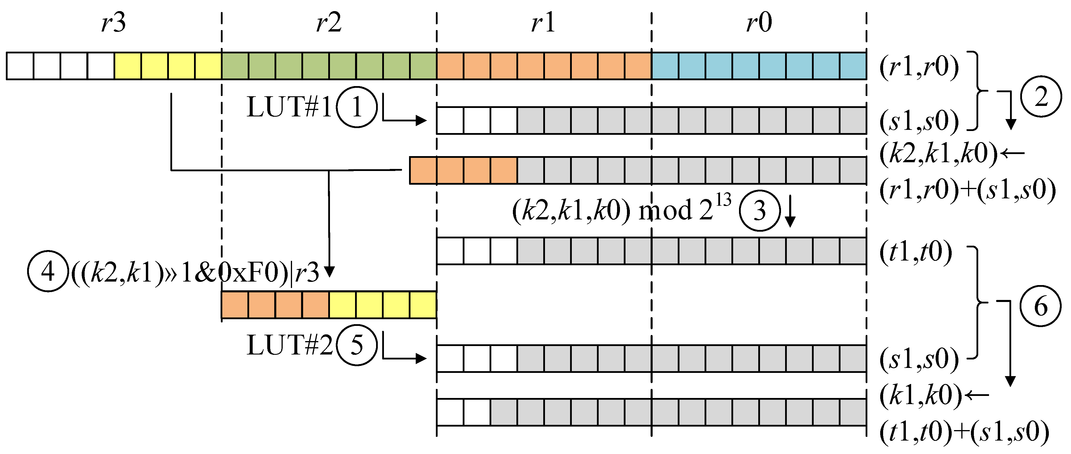
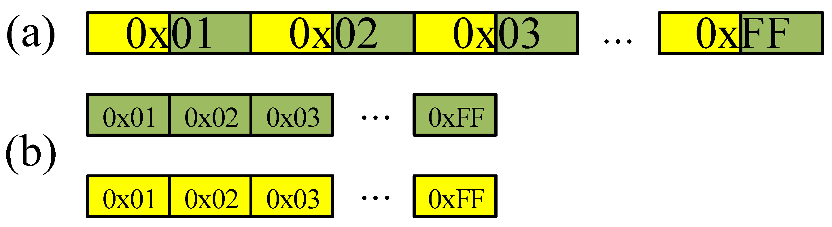
3.1. Look-Up Table-Based Fast Reduction
| Algorithm 1 Iterative Number Theoretic Transform |
| Require: A polynomial of degree and n-th primitive of unity |
| Ensure: Polynomial |
| 1: |
| 2: for i from 2 by to n do |
| 3: , |
| 4: for j from 0 by 1 to do |
| 5: for k from 0 by i to do |
| 6: |
| 7: |
| 8: |
| 9: |
| 10: |
| 11: return a |
3.2. Number Theoretic Transform
| Algorithm 2 LUT-based modular reduction in source code (mod 7681) | |||
| Input: operands R22, R23, R24, R25 | 17: LDI R31, hi8(LUT1_H) | ||
| 18: LPM R23, Z | |||
| Output: results {R24, R25} | |||
| 19: ADD R18, R22 | |||
| 1: CLR R26 | {MOV-and-ADD} | 20: ADC R19, R23 | |
| 2: MUL R24, R22 | 21: ADC R20, R20 | {Register re-use} | |
| 3: MOVW R18, R0 | |||
| 4: MUL R25, R23 | 22: MOV R30, R19 | ||
| 5: MOVW R20, R0 | 23: ANDI R19, 0X1F | ||
| 24: LSR R20 | |||
| 6: MOVW R18, R0 | 25: ROR R30 | ||
| 7: ADD R19, R0 | |||
| 8: MOVW R18, R0 | 26: ANDI R30, 0XF0 | ||
| 9: MOVW R18, R0 | 27: ADD R30, R21 | ||
| 28: LDI R31, hi8(LUT2_L) | {LUT access} | ||
| 10: MOVW R18, R0 | 29: LPM R24, Z | ||
| 11: MOVW R18, R0 | |||
| 12: ADC R20, R1 | 30: LDI R31, hi8(LUT2_H) | ||
| 13: ADC R21, R26 | 31: LPM R25, Z | ||
| 14: MOV R30, R20 | 32: ADD R24, R18 | ||
| 15: LDI R31, hi8(LUT1_L) | {LUT access} | 33: ADC R25, R19 | |
| 16: LPM R22, Z | 34: CLR R1 | ||
| Algorithm 3 LUT-based modular reduction in source code (mod 12,289) | |||
| Input: operands R22, R23, R24, R25 | 17: LDI R31, hi8(LUT1_H) | ||
| 18: LPM R23, Z | |||
| Output: results {R24, R25} | |||
| 19: ADD R18, R22 | |||
| 1: CLR R26 | {MOV-and-ADD} | 20: ADC R19, R23 | |
| 2: MUL R24, R22 | 21: ADC R20, R20 | {Register re-use} | |
| 3: MOVW R18, R0 | |||
| 4: MUL R25, R23 | 22: MOV R30, R19 | ||
| 5: MOVW R20, R0 | 23: ANDI R19, 0X3F | ||
| 24: ANDI R20, 0X01 | |||
| 6: MUL R24, R23 | 25: ANDI R30, 0XC0 | ||
| 7: ADD R19, R0 | |||
| 8: ADC R20, R1 | 26: ADD R30, R21 | ||
| 9: ADC R21, R26 | 27: LDI R31, hi8(LUT2_L) | {LUT access} | |
| 28: ADD R31, R20 | |||
| 10: MUL R25, R22 | 29: LPM R24, Z | ||
| 11: ADD R19, R0 | |||
| 12: ADC R20, R1 | 30: LDI R31, hi8(LUT2_H) | ||
| 13: ADC R21, R26 | 31: ADD R31, R20 | ||
| 32: LPM R25, Z | |||
| 14: MOV R30, R20 | |||
| 15: LDI R31, hi8(LUT1_L) | {LUT access} | 33: ADD R24, R18 | |
| 16: LPM R22, Z | 34: ADC R25, R19 | ||
| 35: CLR R1 | |||
3.2.1. Discrete Gaussian Sampling
3.2.2. AES-Based Pseudo Random Number Generator
4. Performance Evaluation
4.1. Experimental Platform
4.2. Comparison of Modular Multiplication and NTT
4.3. Comparison of Ring-LWE
5. Conclusions
Author Contributions
Funding
Conflicts of Interest
References
- Qiu, L.; Liu, Z.; Pereira, G.C.; Seo, H. Implementing RSA for sensor nodes in smart cities. Pers. Ubiquitous Comput. 2017, 21, 807–813. [Google Scholar] [CrossRef]
- Seo, H.; Kim, H. MoTE-ECC based encryption on MSP430. J. Inf. Commun. Converg. Eng. 2017, 15, 160–164. [Google Scholar]
- Liu, Z.; Huang, X.; Hu, Z.; Khan, M.K.; Seo, H.; Zhou, L. On emerging family of elliptic curves to secure internet of things: ECC comes of age. IEEE Trans. Dependable Secur. Comput. 2017, 14, 237–248. [Google Scholar] [CrossRef]
- Seo, H. Faster ECC over (feat. PMULL). In A Systems Approach to Cyber Security: Proceedings of the 2nd Singapore Cyber-Security R&D Conference (SGCRC 2017); IOS Press: Singapore, 2017; Volume 15, p. 97. [Google Scholar]
- Liu, Z.; Weng, J.; Hu, Z.; Seo, H. Efficient elliptic curve cryptography for embedded devices. Acm Trans. Embed. Comput. Syst. (TECS) 2016, 16, 1–18. [Google Scholar] [CrossRef]
- Seo, H.; Liu, Z.; Großschädl, J.; Kim, H. Efficient arithmetic on ARM-NEON and its application for high-speed RSA implementation. Secur. Commun. Netw. 2016, 9, 5401–5411. [Google Scholar] [CrossRef]
- Liu, Z.; Seo, H.; Großschädl, J.; Kim, H. Efficient implementation of NIST-compliant elliptic curve cryptography for 8-bit AVR-based sensor nodes. IEEE Trans. Inf. Forensics Secur. 2016, 11, 1385–1397. [Google Scholar] [CrossRef]
- Liu, Z.; Seo, H.; Xu, Q. Performance evaluation of twisted Edwards-form elliptic curve cryptography for wireless sensor nodes. Secur. Commun. Netw. 2015, 8, 3301–3310. [Google Scholar] [CrossRef]
- Seo, H.; Liu, Z.; Nogami, Y.; Park, T.; Choi, J.; Zhou, L.; Kim, H. Faster ECC over (feat. NEON). In Proceedings of the International Conference on Information Security and Cryptology, Seoul, Korea, 25–27 November 2015; pp. 169–181. [Google Scholar]
- Liu, Z.; Seo, H.; Hu, Z.; Hunag, X.; Großschädl, J. Efficient implementation of ECDH key exchange for MSP430-based wireless sensor networks. In Proceedings of the 10th ACM Symposium on Information, Computer and Communications Security, Singapore, 14–17 April 2015; pp. 145–153. [Google Scholar]
- Liu, Z.; Seo, H.; Großschädl, J.; Kim, H. Efficient implementation of NIST-compliant elliptic curve cryptography for sensor nodes. In Proceedings of the International Conference on Information and Communications Security, Beijing, China, 20–22 November 2013; pp. 302–317. [Google Scholar]
- Liu, Z.; Longa, P.; Pereira, G.; Reparaz, O.; Seo, H. Four on embedded devices with strong countermeasures against side-channel attacks. IEEE Trans. Dependable Secur. Comput. 2018. [Google Scholar] [CrossRef]
- Zhou, L.; Su, C.; Hu, Z.; Lee, S.; Seo, H. Lightweight implementations of NIST P-256 and SM2 ECC on 8-bit resource-constraint embedded device. Acm Trans. Embed. Comput. Syst. (TECS) 2019, 18, 1–13. [Google Scholar] [CrossRef]
- Seo, H. Compact implementations of Curve Ed448 on low-end IoT platforms. ETRI J. 2019, 41, 863–872. [Google Scholar] [CrossRef]
- Seo, H.; An, K.; Kwon, H.; Hu, Z. Compact Implementation of Modular Multiplication for Special Modulus on MSP430X. In Proceedings of the International Conference on Information Security and Cryptology, Seoul, Korea, 28–30 November 2018; pp. 55–66. [Google Scholar]
- Seo, S.C.; Seo, H. Highly efficient implementation of NIST-compliant Koblitz curve for 8-bit AVR-based sensor nodes. IEEE Access 2018, 6, 67637–67652. [Google Scholar] [CrossRef]
- Liu, Z.; Seo, H. IoT-NUMS: Evaluating NUMS elliptic curve cryptography for IoT platforms. IEEE Trans. Inf. Forensics Secur. 2018, 14, 720–729. [Google Scholar] [CrossRef]
- Seo, H. Compact software implementation of public-key cryptography on MSP430X. Acm Trans. Embed. Comput. Syst. (TECS) 2018, 17, 1–12. [Google Scholar] [CrossRef]
- Liu, Z.; Seo, H.; Castiglione, A.; Choo, K.K.R.; Kim, H. Memory-efficient implementation of elliptic curve cryptography for the Internet-of-Things. IEEE Trans. Dependable Secur. Comput. 2018, 16, 521–529. [Google Scholar] [CrossRef]
- Shor, P.W. Algorithms for quantum computation: Discrete logarithms and factoring. In Proceedings of the 35th Annual Symposium on Foundations of Computer Science, Santa Fe, NM, USA, 20–22 November 1994; pp. 124–134. [Google Scholar]
- Regev, O. On lattices, learning with errors, random linear codes, and cryptography. J. Acm (JACM) 2009, 56, 1–40. [Google Scholar] [CrossRef]
- Lyubashevsky, V.; Peikert, C.; Regev, O. On ideal lattices and learning with errors over rings. In Proceedings of the Annual International Conference on the Theory and Applications of Cryptographic Techniques, Nice, French Riviera, France, 30 May–3 June 2010; pp. 1–23. [Google Scholar]
- Oder, T.; Pöppelmann, T.; Güneysu, T. Beyond ECDSA and RSA: Lattice-based digital signatures on constrained devices. Proceeedings of the 2014 51st ACM/EDAC/IEEE Design Automation Conference (DAC), San Francisco, CA, USA, 1–5 June 2014; pp. 1–6. [Google Scholar]
- De Clercq, R.; Roy, S.S.; Vercauteren, F.; Verbauwhede, I. Efficient software implementation of ring-LWE encryption. 2015 Design, Automation & Test in Europe Conference & Exhibition (DATE), Grenoble, France, 9–13 March 2015; pp. 339–344. [Google Scholar]
- Boorghany, A.; Sarmadi, S.B.; Jalili, R. On constrained implementation of lattice-based cryptographic primitives and schemes on smart cards. Acm Trans. Embed. Comput. Syst. (TECS) 2015, 14, 1–25. [Google Scholar] [CrossRef]
- Boorghany, A.; Jalili, R. Implementation and comparison of lattice-based identification protocols on smart cards and microcontrollers. Iacr Cryptol. Eprint Arch. 2014, 2014, 78. [Google Scholar]
- Pöppelmann, T.; Oder, T.; Güneysu, T. High-performance ideal lattice-based cryptography on 8-bit ATxmega microcontrollers. In Proceedings of the International Conference on Cryptology and Information Security in Latin America, Guadalajara, Mexico, 23–26 August 2015; pp. 346–365. [Google Scholar]
- Liu, Z.; Seo, H.; Roy, S.S.; Großschädl, J.; Kim, H.; Verbauwhede, I. Efficient Ring-LWE encryption on 8-bit AVR processors. In Proceedings of the International Workshop on Cryptographic Hardware and Embedded Systems, Saint Malo, France, 13–16 September 2015; pp. 663–682. [Google Scholar]
- Liu, Z.; Pöppelmann, T.; Oder, T.; Seo, H.; Roy, S.S.; Güneysu, T.; Großschädl, J.; Kim, H.; Verbauwhede, I. High-performance ideal lattice-based cryptography on 8-bit AVR microcontrollers. Acm Trans. Embed. Comput. Syst. (TECS) 2017, 16, 1–24. [Google Scholar] [CrossRef]
- Seo, H.; Liu, Z.; Park, T.; Kwon, H.; Lee, S.; Kim, H. Secure number theoretic transform and speed record for Ring-LWE encryption on embedded processors. In Proceedings of the International Conference on Information Security and Cryptology, Seoul, Korea, 29 November–1 December 2017; pp. 175–188. [Google Scholar]
- Seo, H.; Kwon, H.; Kwon, Y.; Kim, K.; Choi, S.; Kim, H.; Jang, K. Ring-LWE on 8-Bit AVR embedded processor. In Proceedings of the International Workshop on Information Security Applications, Jeju Island, Korea, 21–24 August 2019; pp. 315–327. [Google Scholar]
- Kim, K.; Choi, S.; Kwon, H.; Liu, Z.; Seo, H. FACE-LIGHT: Fast AES-CTR mode encryption for low-end microcontrollers. In Proceedings of the International Conference on Information Security and Cryptology, Seoul, Korea, 4–6 December 2019. [Google Scholar]
- Bos, J.; Ducas, L.; Kiltz, E.; Lepoint, T.; Lyubashevsky, V.; Schanck, J.M.; Schwabe, P.; Seiler, G.; Stehlé, D. CRYSTALS-Kyber: A CCA-secure module-lattice-based KEM. In Proceedings of the 2018 IEEE European Symposium on Security and Privacy (EuroS&P), London, UK, 24–26 April 2018; pp. 353–367. [Google Scholar]
- Alkim, E.; Ducas, L.; Pöppelmann, T.; Schwabe, P. Post-quantum key exchange—A new hope. In Proceedings of the 25th USENIX Security Symposium (USENIX Security 16), Austin, TX, USA, 10–12 August 2016; pp. 327–343. [Google Scholar]
- Roy, S.S.; Reparaz, O.; Vercauteren, F.; Verbauwhede, I. Compact and side channel secure discrete Gaussian sampling. IACR Cryptol. Eprint Arch. 2014, 2014, 591. [Google Scholar]
- Pessl, P. Analyzing the shuffling side-channel countermeasure for lattice-based signatures. In Proceedings of the International Conference on Cryptology in India, Kolkata, India, 11–14 December 2016; pp. 153–170. [Google Scholar]


| Implementation | 128-bit Security | 256-bit Security | ||||
|---|---|---|---|---|---|---|
| MOD MUL | NTT | Const | Mod MUL | NTT | Const | |
| Boorghany et al. [26] | N/A | 1,216,000 | – | N/A | 2,207,787 | – |
| Boorghany et al. [25] | N/A | 754,668 | – | N/A | N/A | – |
| Pöppelmann et al. [27] | N/A | 334,646 | – | N/A | 855,595 | – |
| Liu et al. [28] | N/A | 193,731 | – | N/A | 441,572 | – |
| Liu et al. [29] | 73 | 194,145 | √ | 70 | 516,971 | √ |
| Seo et al. [30] | 57 | 158,607 | √ | 66 | 403,224 | √ |
| This work | 46 | 144,325 | √ | 47 | 344,288 | √ |
| Security Level | n | q | |
|---|---|---|---|
| 128-bit | 256 | 7681 | |
| 256-bit | 512 | 12,289 |
| Implementation | NTT/FFT | Key-Gen | Enc | Secure | PRNG |
|---|---|---|---|---|---|
| Implementations of 128-bit security level | |||||
| Boorghany et al. [26] | 1,216,000 | N/A | 5,024,000 | – | 128-bit AES H/W |
| Boorghany et al. [25] | 754,668 | N/A | 3,042,675 | – | 56-bit DES S/W |
| Pöppelmann et al. [27] | 334,646 | N/A | 1,314,977 | – | 128-bit AES H/W |
| Liu et al. [28] | 193,731 | 589,900 | 671,628 | – | 128-bit AES H/W |
| Liu et al. [29] | 194,145 | N/A | 796,872 | √ | 128-bit AES H/W |
| Seo et al. [30] | 158,607 | N/A | 680,796 | √ | 128-bit AES H/W |
| This work (H/W) | 144,325 | 524,211 | 659,603 | √ | 128-bit AES H/W |
| Implementations of 256-bit security level | |||||
| Boorghany et al. [25] | 2,207,787 | N/A | N/A | – | 56-bit DES S/W |
| Pöppelmann et al. [27] | 855,595 | N/A | 3,279,142 | – | 128-bit AES H/W |
| Liu et al. [28] | 441,572 | 2,165,239 | 2,617,459 | – | 128-bit AES S/W |
| Liu et al. [29] | 516,971 | N/A | 1,975,806 | √ | 128-bit AES H/W |
| Seo et al. [30] | 403,224 | N/A | 1,754,064 | √ | 128-bit AES H/W |
| This work (H/W) | 344,288 | 1,325,171 | 1,430,601 | √ | 128-bit AES H/W |
| This work (S/W) | 344,288 | 1,775,475 | 2,042,474 | √ | 256-bit AES S/W |
© 2020 by the authors. Licensee MDPI, Basel, Switzerland. This article is an open access article distributed under the terms and conditions of the Creative Commons Attribution (CC BY) license (http://creativecommons.org/licenses/by/4.0/).
Share and Cite
Seo, H.; Kwon, H.; Kwon, Y.; Kim, K.; Choi, S.; Kim, H.; Jang, K. Fast Number Theoretic Transform for Ring-LWE on 8-bit AVR Embedded Processor. Sensors 2020, 20, 2039. https://doi.org/10.3390/s20072039
Seo H, Kwon H, Kwon Y, Kim K, Choi S, Kim H, Jang K. Fast Number Theoretic Transform for Ring-LWE on 8-bit AVR Embedded Processor. Sensors. 2020; 20(7):2039. https://doi.org/10.3390/s20072039
Chicago/Turabian StyleSeo, Hwajeong, Hyeokdong Kwon, Yongbeen Kwon, Kyungho Kim, Seungju Choi, Hyunjun Kim, and Kyoungbae Jang. 2020. "Fast Number Theoretic Transform for Ring-LWE on 8-bit AVR Embedded Processor" Sensors 20, no. 7: 2039. https://doi.org/10.3390/s20072039
APA StyleSeo, H., Kwon, H., Kwon, Y., Kim, K., Choi, S., Kim, H., & Jang, K. (2020). Fast Number Theoretic Transform for Ring-LWE on 8-bit AVR Embedded Processor. Sensors, 20(7), 2039. https://doi.org/10.3390/s20072039