High Sensitive Biosensors Based on the Coupling Between Surface Plasmon Polaritons on Titanium Nitride and a Planar Waveguide Mode

Abstract
1. Introduction
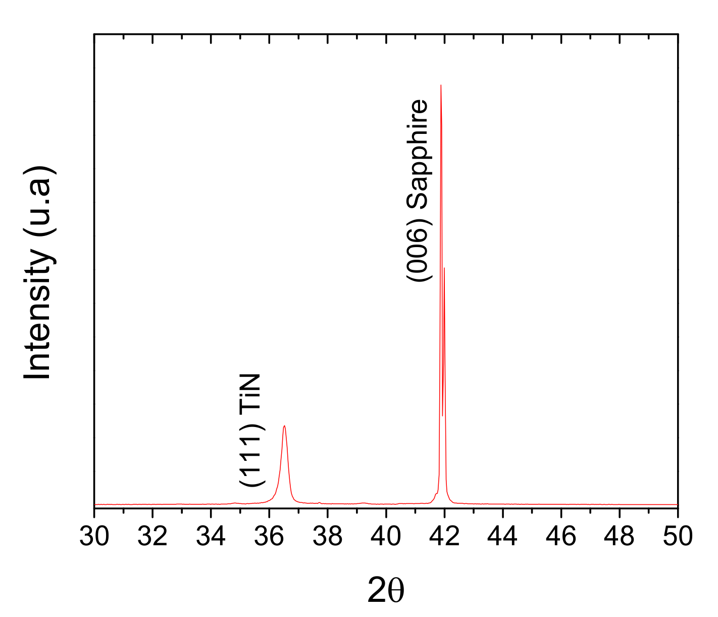
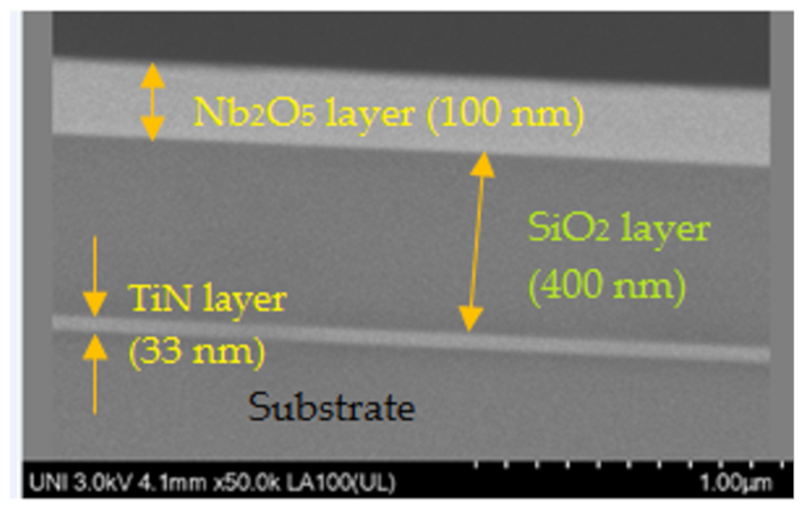
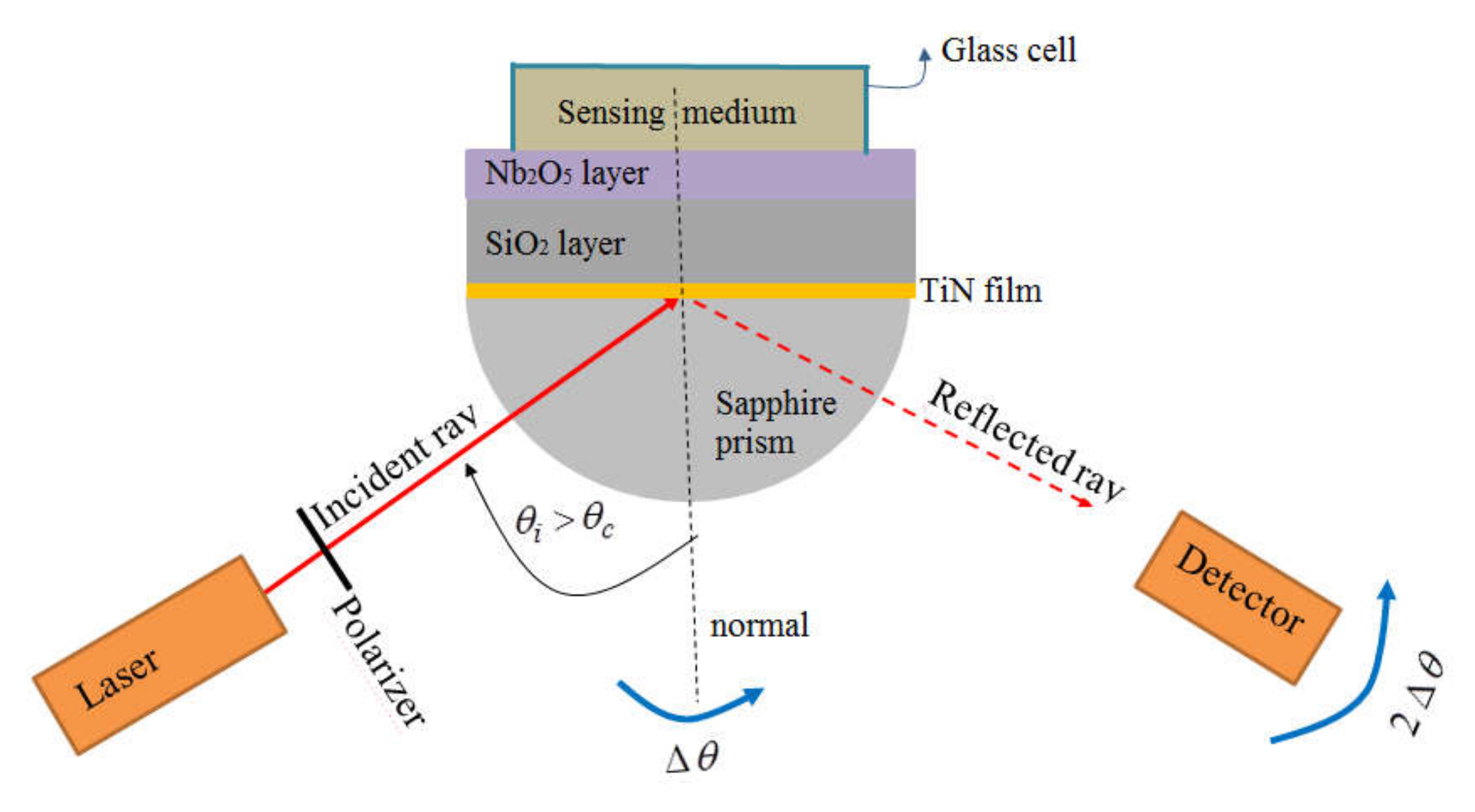
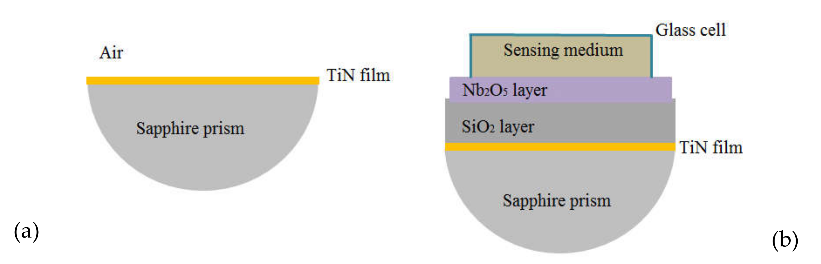
2. Materials and Methods
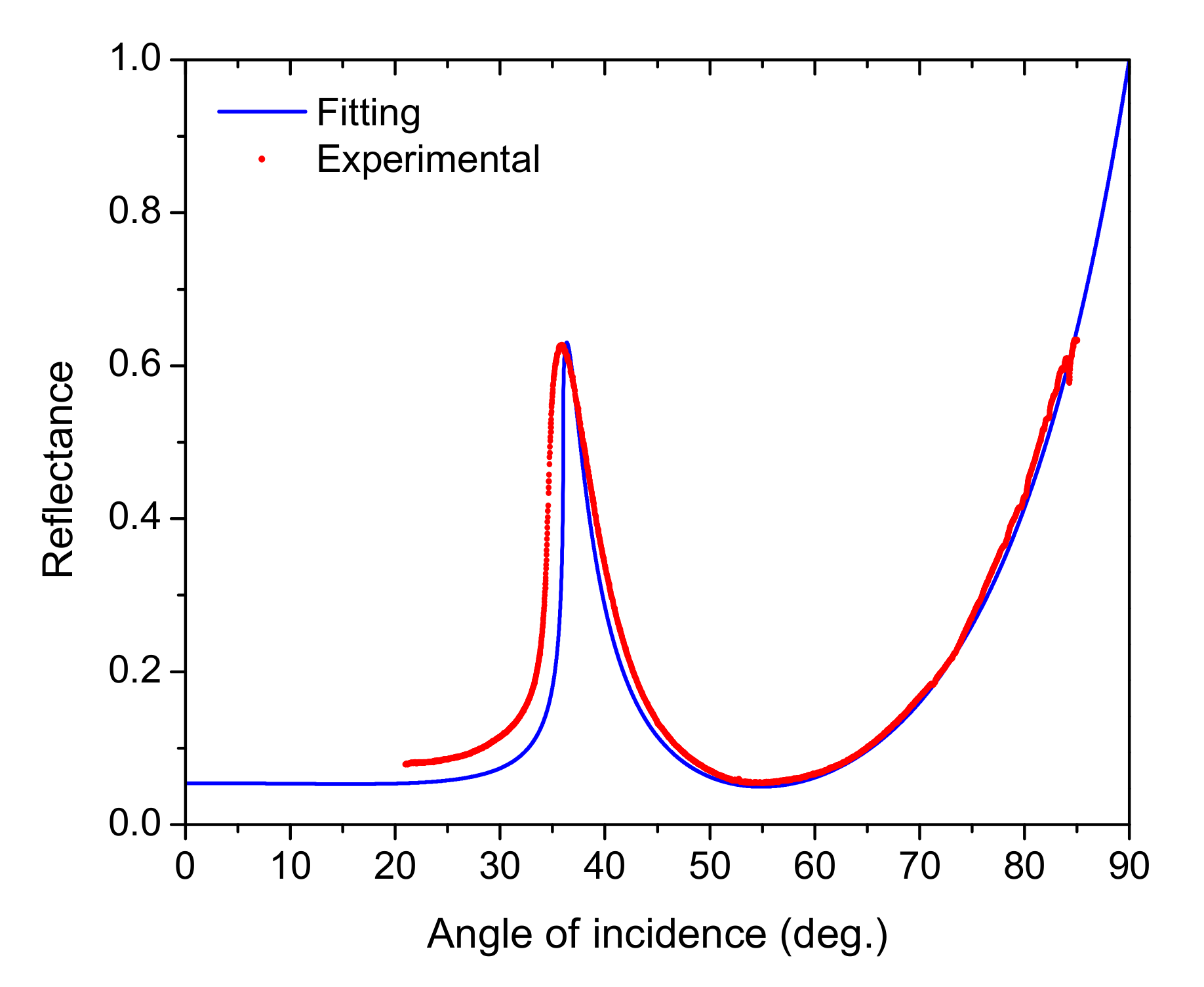
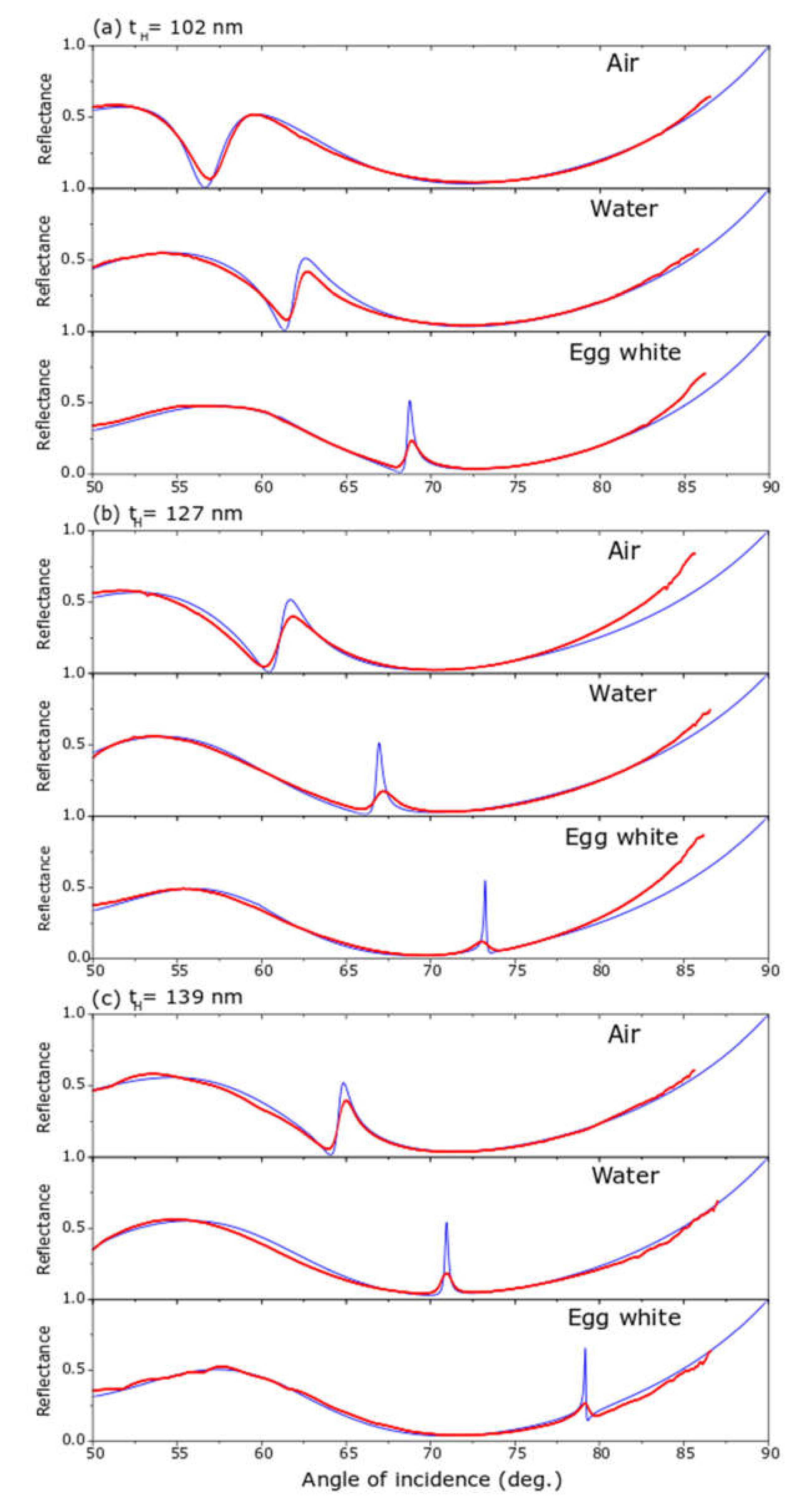
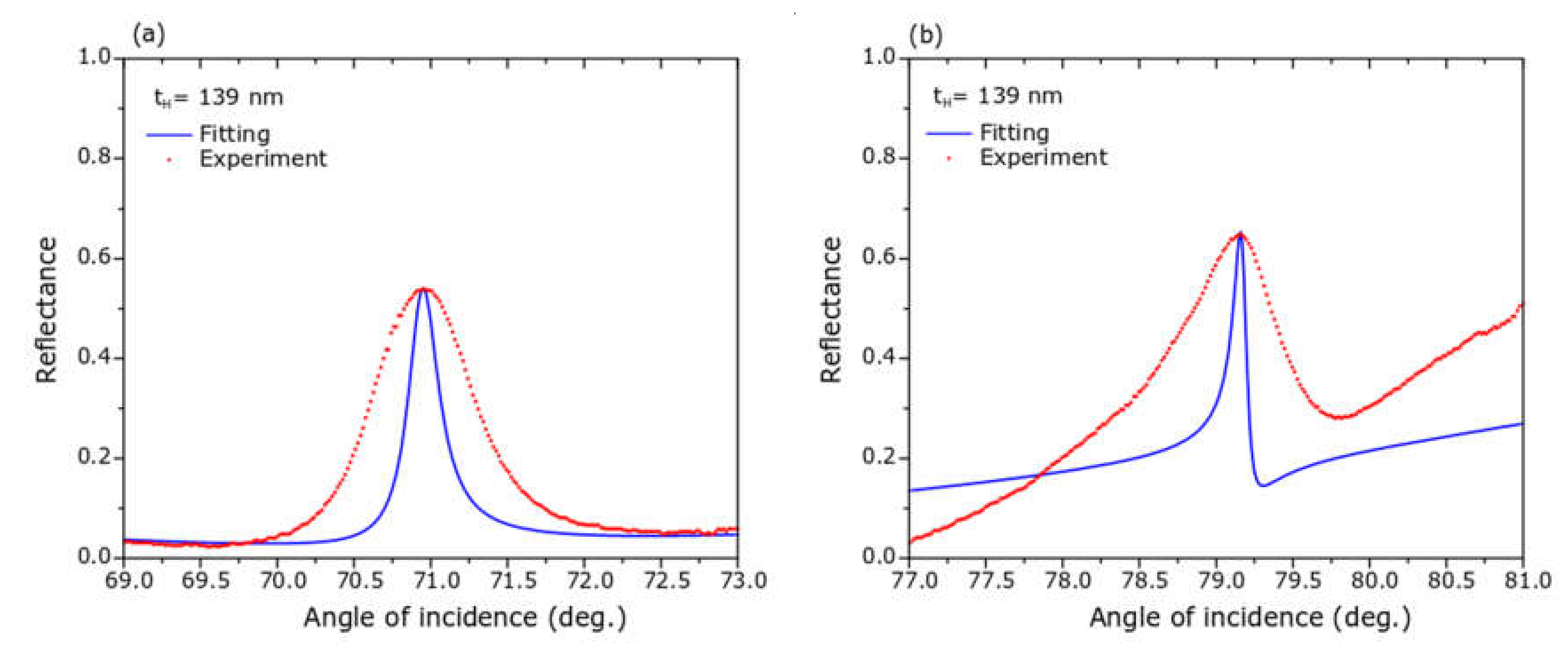
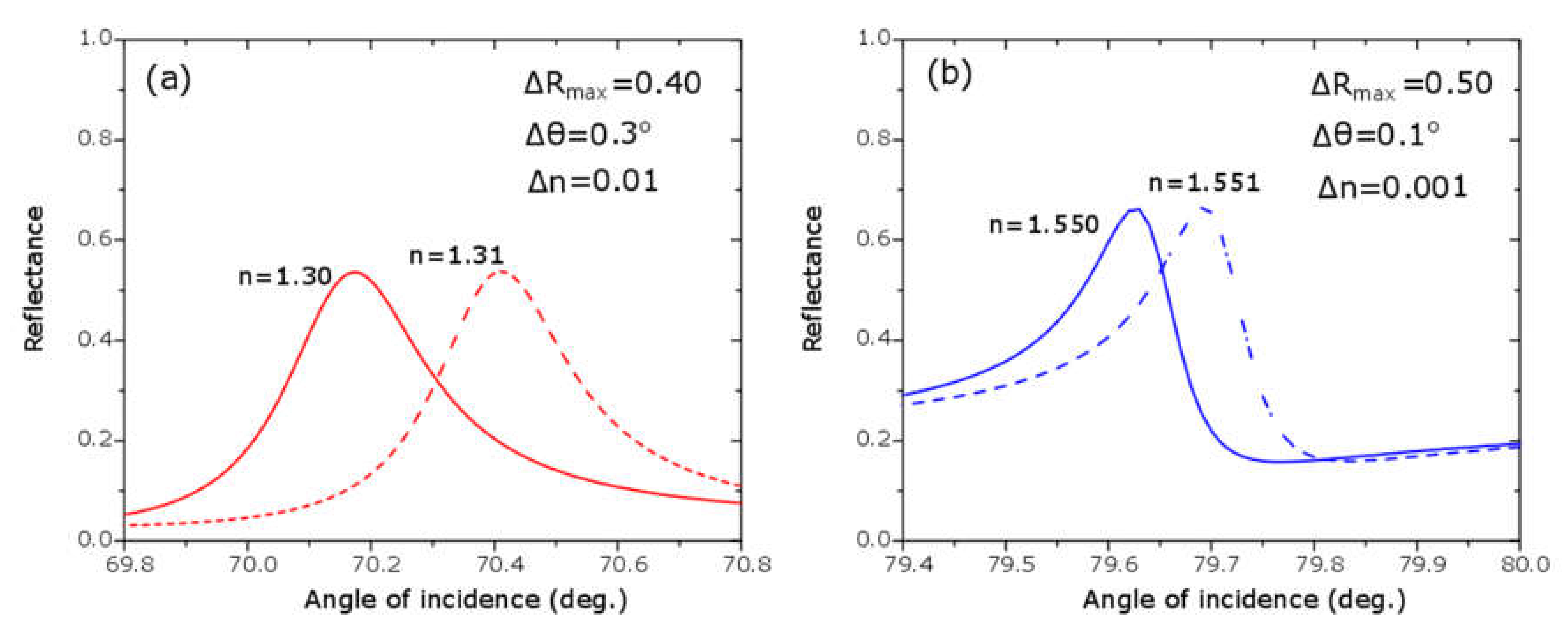
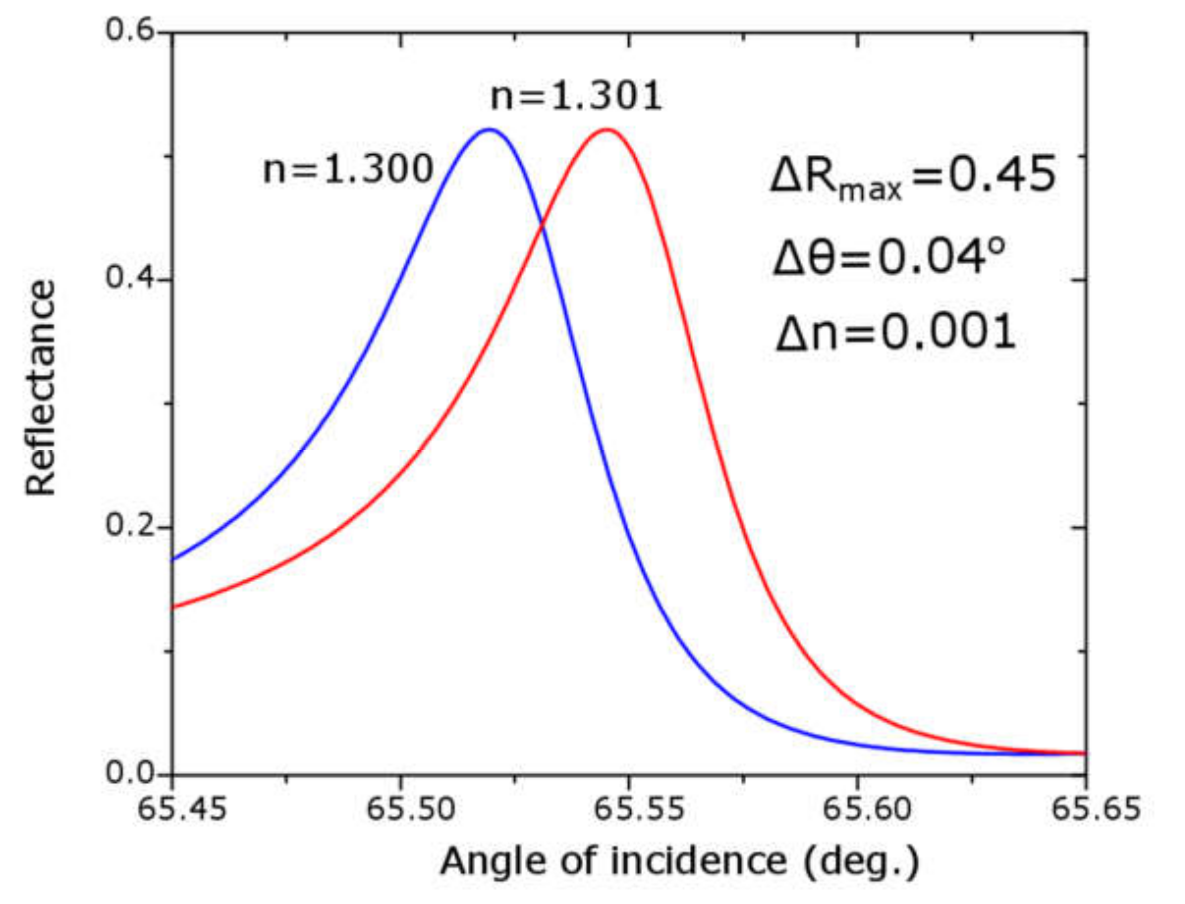
3. Results and Discussion
4. Conclusions
Author Contributions
Funding
Acknowledgments
Conflicts of Interest
References
- Burke, J.J.; Stegeman, G.I.; Tamir, T. Surface-polariton-like waves guided by thin, lossy metal films. Phys. Rev. B 1986, 33, 5186–5201. [Google Scholar] [CrossRef] [PubMed]
- Maier, S.A. Plasmonics: Fundamentals and Applications; Springer Science + Business Media LLC: New York, NY, USA, 2007. [Google Scholar]
- Kretschmann, E. The determination of the optical constants of metals by excitation of surface plasmons. Z. Phys. 1971, 241, 313–324. [Google Scholar] [CrossRef]
- Nylander, C.; Liedberg, B.; Lind, T. Gas detection by means of surface plasmon resonance. Sens. Actuators 1982, 3, 79–88. [Google Scholar] [CrossRef]
- Liedberg, B.; Nylander, C.; Lundström, I. Biosensing with surface plasmon resonance- how it all started. Biosens. Bioelectron. 1995, 10, 1–9. [Google Scholar] [CrossRef]
- Salamon, Z.; Macleod, A.H.; Tollin, G. Coupled plasmon-waveguide resonators: A new spectroscopy tool for probing proteolipid film structure and properties. Biophys. J. 1997, 73, 2791–2797. [Google Scholar] [CrossRef]
- Otto, A. Excitation of nonradiative surface plasmon waves in silver by the method of frustrated total reflectance. Z. Für Phys. 1968, 216, 398–410. [Google Scholar] [CrossRef]
- Devaux, E.; Ebessen, T.W.; Weeber, J.-C.; Dereux, A. Launching and decoupling surface plasmons via micro-gratings. Appl. Phys. Lett. 2003, 83, 4936–4938. [Google Scholar] [CrossRef]
- Stegeman, G.I.; Wallis, R.F.; Maradudin, A.A. Excitation of surface polaritons by end-fire coupling. Opt. Lett. 1983, 8, 386–388. [Google Scholar] [CrossRef]
- Pluchery, O.; Vayron, R.; Van, K.-H. Laboratory experiments for exploring the surface plasmon resonance. Eur. J. Phys. 2011, 32, 585–599. [Google Scholar] [CrossRef]
- Gwon, H.R.; Lee, S.H. Spectral and angular responses of surface plasmon resonance based on the Kretschmann prism configuration. Mater. Trans. 2010, 51, 1150–1155. [Google Scholar] [CrossRef]
- Hayashi, S.; Nesterenko, D.V.; Sekkat, Z. Waveguide-coupled surface plasmon resonance sensor structures: Fano lineshape engineering for ultrahigh-resonance sensing. J. Phys. D 2015, 48, 1–11. [Google Scholar] [CrossRef]
- Hayashi, S.; Nesterenko, D.V.; Sekkat, Z. Fano resonance and plasmon-induced transparency in waveguide-coupled surface plasmon resonance sensors. Appl. Phys. Express 2015, 8, 022201. [Google Scholar] [CrossRef]
- Nesterenko, D.V.; Hayashi, S.; Sekkat, Z. Extremely narrow resonances, giant sensitivity and field enhancement in low-loss waveguide sensors. J. Opt. 2016, 18, 1–12. [Google Scholar] [CrossRef]
- Hayashi, S.; Nesterenko, D.V.; Rahmouni, A.; Sekkat, Z. Observation of Fano line shapes arising from coupling between surface plasmon polariton and waveguide modes. Appl. Phys. Lett. 2016, 108, 051101. [Google Scholar] [CrossRef]
- Sekkat, Z.; Hayashi, S.; Nesterenko, D.V.; Rahmouni, A.; Refki, S.; Ishitobi, H.; Ynouye, Y.; Kawata, S. Plasmonic coupled modes in metal-dielectric multilayer structures: Fano resonance and field enhancement. Opt. Express 2016, 24, 20080. [Google Scholar] [CrossRef] [PubMed]
- Bera, M.; Ray, M. Coupled plasmonic assisted progressive multiple resonance for material dielectric characterization. Opt. Eng. 2011, 50, 103801. [Google Scholar] [CrossRef]
- Boller, K.-J.; Imamoglu, A.; Harris, E.S. Observation of electromagnetically induced transparency. Phys. Rev. Lett. 1991, 66, 2593–2596. [Google Scholar] [CrossRef]
- Harris, S.E. Electromagnetically induced transpartency. Phys. Today 1997, 50, 36–42. [Google Scholar] [CrossRef]
- Fleischhauer, M.; Imamoglu, A.; Marangos, J.P. Electromagnetic induced transparency: Optics in coherent madia. Rev. Mod. Phys. 2005, 77, 633–673. [Google Scholar] [CrossRef]
- Fano, U. Effects of configuration interaction on intensities and phase shifts. Phys. Rev. 1961, 124, 1866–1878. [Google Scholar] [CrossRef]
- Li, Y.; Yuan, Y.; Peng, X.; Song, J.; Liu, J.; Qu, J. An ultrasensitive Fano resonance biosensor using two dimensional hexagonal boron nitride nanosheets: Theoretical analysis. RSC Adv. 2019, 9, 29805–29812. [Google Scholar] [CrossRef]
- Zheng, G.; Zou, X.; Chen, Y.; Xu, L.; Rao, W. Fano resonance in graphene-MoS2 heterostruture-based surface plasmon resonance biosensor and its potential applications. Opt. Mater. 2017, 66, 171–178. [Google Scholar] [CrossRef]
- Grotewohl, H.; Deutsch, M. Tunable geometric fano reosnances based in a metal/insulator stack. J. Opt. 2015, 17, 085003. [Google Scholar] [CrossRef][Green Version]
- Ruan, B.; Guo, J.; Wu, L.; Zhu, J.; You, Q.; Dai, X.; Xiang, Y. Ultrasenssitive terahertz biosensors based on Fano resonance of a graphene/waveguide hybrid structure. Sensors 2017, 1924. [Google Scholar] [CrossRef] [PubMed]
- Nesterenko, D.V.; Hayashi, S.; Sekkat, Z. Assymetric surface plasma resonance revisited as Fano resonance. Phys. Rev. B. 2018, 97, 235437. [Google Scholar] [CrossRef]
- Ruan, B.; You, Q.; Zhu, J.; Wu, L.; Guo, J.; Dai, X.; Xiang, Y. Fano resonance in double waveguides with grapheme and ultrasensitive biosensor. Opt. Express 2018, 26, 16884. [Google Scholar] [CrossRef]
- Hayashi, S.; Fujiwara, Y.; Kang, B.; Fujii, M.; Nesterenko, D.V.; Sekkat, Z. Line shape engineering of sharp Fano resonance in Al-based metal-dielectric multilayer structure. J. Appl. Phys. 2017, 122, 163103. [Google Scholar] [CrossRef]
- Zheng, G.; Cong, J.; Xu, L.; Wang, J. High-resolution surface plasmon resonance sensor with Fano resonance in waveguide-coupled multilayer structures. Appl. Phys. Express 2017, 10, 042202. [Google Scholar] [CrossRef]
- Kang, B.; Fujii, M.; Nesterenko, D.V.; Sekkat, Z.; Hayashi, S. Fano resonances in near-field absorption in all dielectric multilayer structures. J. Opt. 2018, 20, 125003. [Google Scholar] [CrossRef]
- Hertzing, A.A.; Guler, U.; Zhou, X.; Boltasseva, A.; Shalaev, V.; Norris, T.B. Electron energy loss spectroscopy of plasmon resonances in titanium nitride thin films. Appl. Phys. Lett. 2016, 108, 171107. [Google Scholar] [CrossRef]
- Hibbins, A.P.; Sambles, J.R.; Lawrence, C.R. Surface plasmon-polariton study of the optical dielectric function of titanium nitride. J. Mod. Opt. 1998, 2051–2062. [Google Scholar] [CrossRef]
- Naik, G.V.; Schroeder, J.L.; Ni, X.; Kildishev, A.V.; Sands, T.D.; Boltasseva, A. Titanium nitride as a plasmonic material for visible and near-infrared wavelenghts. Opt. Mater. Express 2012, 2, 478–489. [Google Scholar] [CrossRef]
- Kinsey, N.; Ferrera, M.; Naik, G.V.; Babicheva, V.E.; Shalaev, V.M.; Boltasseva, A. Experimental demonstration of titanium nitride plasmonic interconnects. Opt. Express 2014, 22, 12238. [Google Scholar] [CrossRef] [PubMed]
- Patsalas, P.; Kalfagiannis, N.; Kassavetis, S. Optical properties and plasmonic performance of titanium nitride. Materials 2015, 8, 3128–3154. [Google Scholar] [CrossRef]
- Chen, N.C.; Lien, W.C.; Liu, C.R.; Huang, Y.L.; Chou, C.; Chang, S.Y.; Ho, C.W. Excitation of surface plasma wave at TiN/air interface in the Kretschmann geometry. J. Appl. Phys. 2011, 109, 043104. [Google Scholar] [CrossRef]
- Jeyachandran, Y.L.; Narayandas, S.K.; Karunagaran, B.; Mangalaraj, D. Properties of titanium nitride films prepared by dc magnetron sputtering. Mater. Sci. Eng. A 2007, 445, 223–236. [Google Scholar] [CrossRef]
- Macleod, H.A. Thin-Film Optical Filters, 4th ed.; CRC Press: Boca Raton, FL, USA, 2010; pp. 42–46. [Google Scholar]
- José, M.C.; Fernando, A.L.; Fernando, J.L. Electromagnetic Optics Vol. II Materials and Applications; Addison Wesley/Universidad Autónoma de Madrid: Madrid, Spain, 2000; pp. 209–259. [Google Scholar]
- Homola, J.; Yee, S.S.; Gauglitz, G. Surface Plasmon resonance sensors: Review. Sens. Actuators B 1999, 54, 3–15. [Google Scholar] [CrossRef]


| Material | Thickness | n | k |
|---|---|---|---|
| Air | Semi infinite | 1.0 | 0 |
| Titanium nitride | 24 nm | 1.36 | 2.29 |
| Sapphire | Semi infinite | 1.77 | 0 |
| Sensor | Material | Thickness (nm) | n | k |
|---|---|---|---|---|
| A | TiN | 33 | 1.22 | 2.67 |
| A | SiO2 | 399 | 1.49 | 0 |
| A | Nb205 | 102 | 2.2 | 0 |
| A | Air | semi infinite | 1 | 0 |
| A | Water | semi infinite | 1.33 | 0 |
| A | dried egg white | semi infinite | 1.55 | 0 |
| B | Material | thickness | n | k |
| B | TiN | 33 | 1.22 | 2.67 |
| B | SiO2 | 399 | 1.49 | 0 |
| B | Nb205 | 127 | 2.2 | 0 |
| B | Air | semi infinite | 1 | 0 |
| B | Water | semi infinite | 1.33 | 0 |
| B | dried egg white | semi infinite | 1.55 | 0 |
| C | Material | thickness | n | k |
| C | TiN | 33 | 1.22 | 2.67 |
| C | SiO2 | 399 | 1.49 | 0 |
| C | Nb205 | 139 | 2.2 | 0 |
| C | Air | semi infinite | 1 | 0 |
| C | Water | semi infinite | 1.3317 | 0 |
| C | dried egg white | semi infinite | 1.55 | 0 |
© 2020 by the authors. Licensee MDPI, Basel, Switzerland. This article is an open access article distributed under the terms and conditions of the Creative Commons Attribution (CC BY) license (http://creativecommons.org/licenses/by/4.0/).
Share and Cite
Asencios, J.; Moro, R.; Luyo, C.; Talledo, A. High Sensitive Biosensors Based on the Coupling Between Surface Plasmon Polaritons on Titanium Nitride and a Planar Waveguide Mode. Sensors 2020, 20, 1784. https://doi.org/10.3390/s20061784
Asencios J, Moro R, Luyo C, Talledo A. High Sensitive Biosensors Based on the Coupling Between Surface Plasmon Polaritons on Titanium Nitride and a Planar Waveguide Mode. Sensors. 2020; 20(6):1784. https://doi.org/10.3390/s20061784
Chicago/Turabian StyleAsencios, Junior, Ramiro Moro, Clemente Luyo, and Arturo Talledo. 2020. "High Sensitive Biosensors Based on the Coupling Between Surface Plasmon Polaritons on Titanium Nitride and a Planar Waveguide Mode" Sensors 20, no. 6: 1784. https://doi.org/10.3390/s20061784
APA StyleAsencios, J., Moro, R., Luyo, C., & Talledo, A. (2020). High Sensitive Biosensors Based on the Coupling Between Surface Plasmon Polaritons on Titanium Nitride and a Planar Waveguide Mode. Sensors, 20(6), 1784. https://doi.org/10.3390/s20061784