A Microwave Platform for Reliable and Instant Interconnecting Combined with Microwave-Microfluidic Interdigital Capacitor Chips for Sensing Applications †

 , , , and
Abstract
1. Introduction
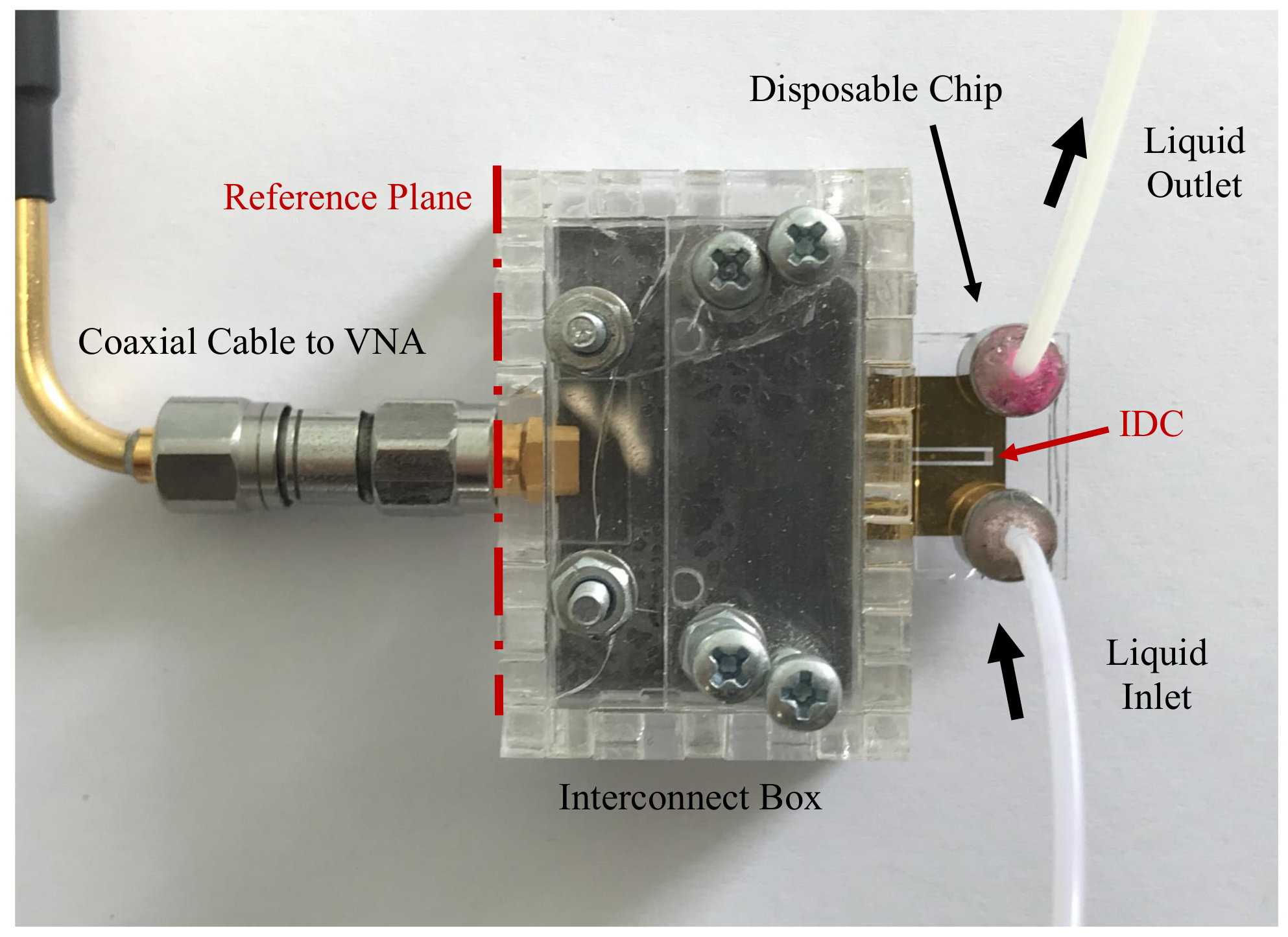
2. Interconnect Box
2.1. Manufacturing
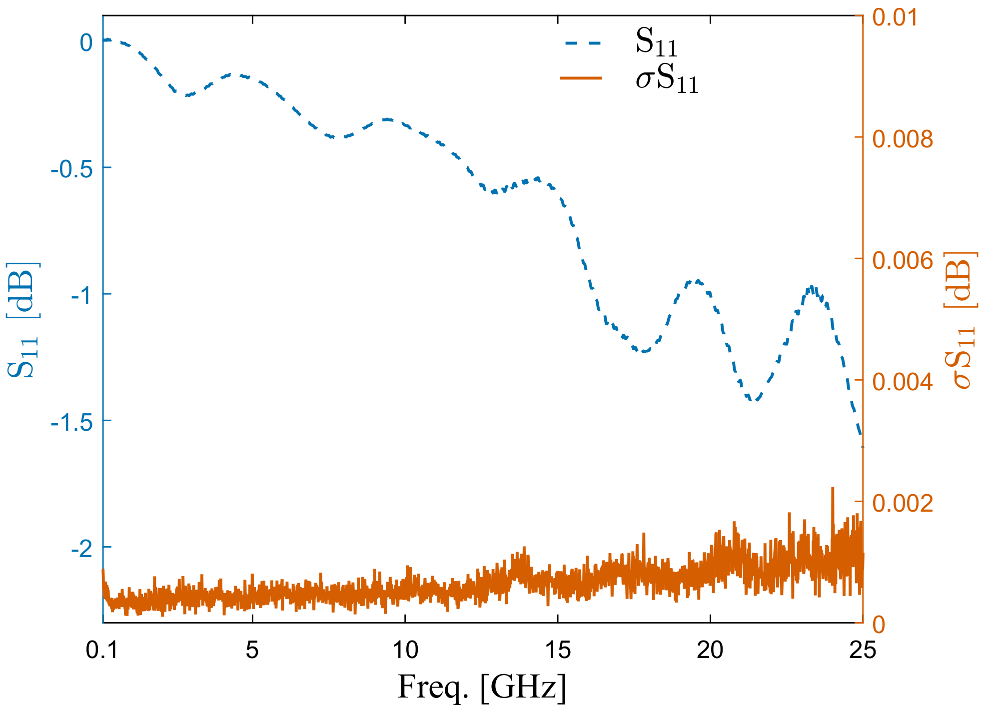
2.2. Electrical Characteristics
3. Application for Microwave-Microfluidic Sensors
3.1. Contact Stability and Repeatability
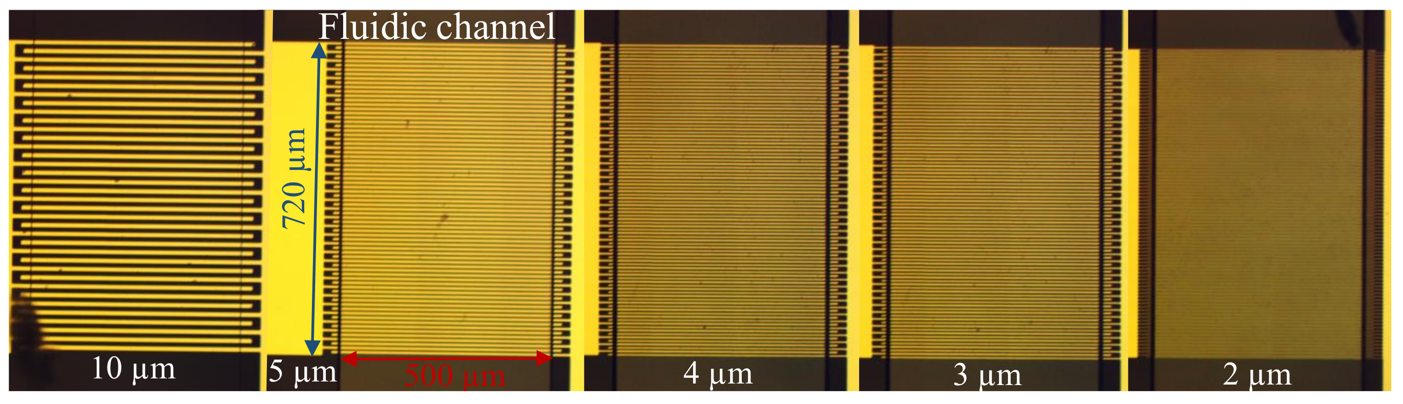
3.2. Quartz Chip Design
3.3. Measurement Results and Permittivity Extraction
4. Conclusions
Author Contributions
Funding
Acknowledgments
Conflicts of Interest
Abbreviations
| CPW | co-planar waveguide |
| DI | deionized |
| HUVEC | human umbilical vein endothelial cells |
| ICB | interconnect box |
| IDC | interdigital capacitor |
| IPA | isopropanol |
| MOF | metal–organic frameworks |
| MOS | metal-oxide-semiconductor |
| PCB | printed circuit board |
| PDMS | polydimethysiloxane |
| PMMA | polymethylmethacrylate |
| SIW | substrate integrated waveguide |
| SMA | subminiature type A |
| SOLT | short open load thru |
| VNA | vector network analyzer |
References
- Whitesides, G. The origins and the future of microfluidics. Nature 2006, 442, 368–373. [Google Scholar] [CrossRef] [PubMed]
- Wyatt Shields, C.; Reyes, C.; Lopez, G. Microfluidic cell sorting: A review of the advances in the separation of cells from debulking to rare cell isolation. Lab Chip 2015, 15, 1230–1249. [Google Scholar] [CrossRef] [PubMed]
- Bareither, R.; Pollard, D. A review of advanced small-scale parallel bioreactor technology for accelerated process development: Current state and future need. Biotechnol. Prog. 2010, 27, 2–14. [Google Scholar] [CrossRef] [PubMed]
- Liu, S. Microwave-Microfluidics: Sensor, Fluid Metrology, and Vector-Network-Analyzer Calibrations. Ph.D. Thesis, KU Leuven, Leuven, Belgium, 2016. [Google Scholar]
- Booth, J.; Orloff, N.; Mateu, J.; Janezic, M.; Rinehart, M.; Beall, J. Quantitative permittivity measurements of nanoliter liquid volumes in microfluidic channels to 40 GHz. IEEE Tran. Instrum. Meas. 2010, 59, 3279–3288. [Google Scholar] [CrossRef]
- Liu, S.; Ocket, I.; Barmuta, P.; Markovic, T.; Lewandowski, A.; Schreurs, D.; Nauwelaers, B. Broadband dielectric spectroscopy calibration using calibration liquids with unknown permittivity. In Proceedings of the 84th ARFTG Microwave Measurement Conference, Boulder, CO, USA, 2–5 December 2014; pp. 1–5. [Google Scholar]
- Liu, S.; Orloff, N.; Little, C.; Zhao, W.; Booth, J.; Williams, D.; Ocket, I.; Schreurs, D.; Nauwelaers, B. Hybrid characterization of nanolitre dielectric fluids in a single microfluidic channel up to 110 GHz. IEEE Trans. Microw. Theory Techn. 2017, 65, 5063–5073. [Google Scholar] [CrossRef]
- Grenier, K.; Dubuc, D.; Poleni, P.; Kumemura, M.; Toshiyoshi, H.; Fujii, T.; Fujita, H. Integrated broadband microwave and microfluidic sensor dedicated to bioengineering. IEEE Trans. Microw. Theory Techn. 2009, 57, 3246–3253. [Google Scholar] [CrossRef]
- Tamra, A.; Dubuc, D.; Rols, M.; Grenier, K. Microwave monitoring of single cell monocytes subjected to electroporation. IEEE Trans. Microw. Theory Techn. 2017, 65, 3512–3518. [Google Scholar] [CrossRef]
- Markovic, T.; Bao, J.; Maenhout, G.; Ocket, I.; Nauwelaers, B. An Interdigital Capacitor for Microwave Heating at 25 GHz and Wideband Dielectric Sensing of nL Volumes in Continuous Microfluidics. Sensors 2019, 19, 715. [Google Scholar] [CrossRef]
- Bao, J.; Yan, S.; Markovic, T.; Ocket, I.; Kil, D.; Brancato, L.; Puers, R.; Nauwelaers, B. A 20-GHz microwave miniaturized ring resonator for nL microfluidic sensing Applications. IEEE Sens. Lett. 2019, 3, 4500604. [Google Scholar] [CrossRef]
- Yan, S.; Bao, J.; Ocket, I.; Nauwelaers, B.; Vandenbosch, G. Metamaterial inspired miniaturized SIW resonator for sensor applications. Sensor Actuat. A-Phys. 2018, 283, 313–316. [Google Scholar] [CrossRef]
- Markovic, T.; Liu, S.; Ocket, I.; Nauwelaers, B. A 20 GHz microwave heater for digital microfluidic. Int. J. Microw. Wirel. Technol. 2017, 9, 1591–1596. [Google Scholar] [CrossRef]
- Markovic, T.; Ocket, I.; Jones, B.; Nauwelaers, B. Characterization of a novel microwave heater for continuous flow microfluidics fabricated on high-resistivity silicon. Proccedings of the IEEE MTTS Int. Microw. Symp., San Fransisco, CA, USA, 22–27 May 2016; pp. 1–4. [Google Scholar]
- Markovic, T.; Bao, J.; Ocket, I.; Kil, D.; Brancato, L.; Puers, R.; Nauwelaers, B. Uniplanar microwave heater for digital microfluidics. In Proceedings of the 2017 First IEEE MTT-S International Microwave Bio Conference (IMBioC), Gothenburg, Sweden, 15–17 May 2017; pp. 1–4. [Google Scholar]
- Hu, J.; Tarasov, V.; Agarwal, A.; Kimerling, L.; Carlie, N.; Petit, L.; Richardson, K. Fabrication and testing of planar chalcogenide waveguide integrated microfluidic sensor. Opt. Express 2007, 15, 2307–2314. [Google Scholar] [CrossRef] [PubMed]
- Chen, Y.; Xu, D.; Xu, K.; Zhang, N.; Liu, S.; Zhao, J.; Luo, Q.; Snyman, L.W.; Swart, J.W. Optoelectronic properties analysis of silicon light-emitting diode monolithically integrated in standard CMOS IC. Chin. Phys. B 2019, 28, 107801. [Google Scholar] [CrossRef]
- Xu, K.; Chen, Y.; Okhai, T.A.; Snyman, L.W. Micro optical sensors based on avalanching silicon light-emitting devices monolithically integrated on chips. Opt. Mater. Express 2019, 9, 3985–3997. [Google Scholar] [CrossRef]
- Yoshihara, T.; Yamaguchi, Y.; Hosaka, M.; Takeuchi, T.; Tobita, S. Ratiometric Molecular Sensor for Monitoring Oxygen Levels in Living Cells. Angew. Chem. Int. Ed. 2012, 51, 4148–4151. [Google Scholar] [CrossRef]
- R&D Interconnect Solutions. R&DIS | RD Interconnect Solutions. Available online: http://rdis.com/ (accessed on 14 March 2020).
- Bao, X.; Ocket, I.; Crupi, G.; Schreurs, D.; Bao, J.; Kil, D.; Puers, R.; Nauwelaers, B. A planar one-port microwave microfluidic sensor for microliter liquids characterization. IEEE J-ERM 2018, 2, 10–17. [Google Scholar] [CrossRef]
- Wei, Y.; Sridhar, S. Technique for measuring complex dielectric constants of liquids up to 20 GHz. Rei. Sci. Instrum. 1989, 60, 3041–3046. [Google Scholar] [CrossRef]
- Wei, Y.; Sridhar, S. Radiation-corrected open-ended coax line technique for dielectric measurements of liquids up to 20 GHz. IEEE Trans. Microw. Theory Techn. 1991, 39, 526–531. [Google Scholar] [CrossRef]
- Igreja, R.; Dias, C.J. Analytical evaluation of the interdigital electrodes capacitance for a multi-layered structure. IEEE Sensor Actuat. A-Phys. 2004, 112, 291–301. [Google Scholar] [CrossRef]
- Xu, K. Silicon MOS Optoelectronic Micro-Nano Structure Based on Reverse-Biased PN Junction. Phys. Status Solidi A 2019, 216, 1800868. [Google Scholar] [CrossRef]
- Sheberla, D.; Bachman, J.; Elias, J.; Sun, C.; Yang, S.; Dinca, M. Conductive MOF electrodes for stable supercapacitors with high areal capacitance. Nature Mater. 2017, 16, 220–224. [Google Scholar] [CrossRef] [PubMed]
- Atencia, J.; Cooksey, G.; Jahn, A.; Zook, J.; Vreelanda, W.; Locascioa, L. Magnetic connectors for microfluidic applications. Lab. Chip 2010, 10, 246–249. [Google Scholar] [CrossRef] [PubMed]
- Sato, T.; Buchner, R. Dielectric relaxation spectroscopy of 2-propanol-water mixtures. J. Chem. Phys. 2003, 118, 4606–4613. [Google Scholar] [CrossRef]
- Fuchs, K.; Kaatze, U. Molecular Dynamics of Carbohydrate Aqueous Solutions. Dielectric Relaxation as a Function of Glucose and Fructose Concentration. J. Phys. Chem. B 2001, 105, 2036–2042. [Google Scholar] [CrossRef]
- Rodríguez-Arteche, I.; Cerveny, S.; Alegria, A.; Colmenero, J. Dielectric spectroscopy in the GHz region on fully hydrated zwitterionic amino acids. Phys. Chem. Chem. Phys. 2012, 14, 11352–11362. [Google Scholar] [CrossRef]
- Kang, B.; Park, J.; Cho, J.; Kwon, K.; Lim, S.; Yoon, J.; Cheon, C.; Kim, Y.; Kwon, Y. Novel low-cost planar probes with broadside apertures for nondestructive dielectric measurement of biological materials at microwave frequencies. IEEE Trans. Microw. Theory Techn. 2005, 33, 134–143. [Google Scholar] [CrossRef]


© 2020 by the authors. Licensee MDPI, Basel, Switzerland. This article is an open access article distributed under the terms and conditions of the Creative Commons Attribution (CC BY) license (http://creativecommons.org/licenses/by/4.0/).
Share and Cite
Bao, J.; Maenhout, G.; Markovic, T.; Ocket, I.; Nauwelaers, B. A Microwave Platform for Reliable and Instant Interconnecting Combined with Microwave-Microfluidic Interdigital Capacitor Chips for Sensing Applications. Sensors 2020, 20, 1687. https://doi.org/10.3390/s20061687
Bao J, Maenhout G, Markovic T, Ocket I, Nauwelaers B. A Microwave Platform for Reliable and Instant Interconnecting Combined with Microwave-Microfluidic Interdigital Capacitor Chips for Sensing Applications. Sensors. 2020; 20(6):1687. https://doi.org/10.3390/s20061687
Chicago/Turabian StyleBao, Juncheng, Gertjan Maenhout, Tomislav Markovic, Ilja Ocket, and Bart Nauwelaers. 2020. "A Microwave Platform for Reliable and Instant Interconnecting Combined with Microwave-Microfluidic Interdigital Capacitor Chips for Sensing Applications" Sensors 20, no. 6: 1687. https://doi.org/10.3390/s20061687
APA StyleBao, J., Maenhout, G., Markovic, T., Ocket, I., & Nauwelaers, B. (2020). A Microwave Platform for Reliable and Instant Interconnecting Combined with Microwave-Microfluidic Interdigital Capacitor Chips for Sensing Applications. Sensors, 20(6), 1687. https://doi.org/10.3390/s20061687