Letter

Photoelectric Characteristics of a Large-Area n-MoS2/p-Si Heterojunction Structure Formed through Sulfurization Process

Department of Physics and Research Institute of Natural Science, Hanyang University, Seoul 04763, Korea
*
Author to whom correspondence should be addressed.
Sensors 2020, 20(24), 7340; https://doi.org/10.3390/s20247340
Submission received: 24 November 2020 / Revised: 15 December 2020 / Accepted: 18 December 2020 / Published: 21 December 2020
(This article belongs to the Section Optical Sensors)

Abstract

:
Two-dimensional (2D) materials, such as molybdenum disulfide (MoS2) of the transition metal dichalcogenides family, are widely investigated because of their outstanding electrical and optical properties. However, not much of the 2D materials research completed to date has covered large-area structures comprised of high-quality heterojunction diodes. We fabricated a large-area n-MoS2/p-Si heterojunction structure by sulfurization of MoOx film, which is thermally evaporated on p-type silicon substrate. The n-MoS2/p-Si structure possessed excellent diode characteristics such as ideality factor of 1.53 and rectification ratio in excess of 104. Photoresponsivity and detectivity of the diode showed up to 475 mA/W and 6.5 × 10¹¹ Jones, respectively, in wavelength ranges from visible to near-infrared. The device appeared also the maximum external quantum efficiency of 72%. The rise and decay times of optical transient response were measured about 19.78 ms and 0.99 ms, respectively. These results suggest that the sulfurization process for large-area 2D heterojunction with MoS2 can be applicable to next-generation electronic and optoelectronic devices.

1. Introduction

Two-dimensional (2D) materials have been intensely studied due to their extraordinary electrical and optical properties ever since graphene was first mechanically exfoliated from graphite by using Scotch tape [1]. Because of weak van der Waals force between each layer in the layered structure, 2D materials can be easily exfoliated to thin film. However, the zero bandgap of graphene obstructs its application for semiconductors in electronic and optoelectronic operation [2,3]. Therefore, transition metal dichalcogenides (TMDs) have aroused significant interest due to their appropriate band gap for applications such as field-effect transistors (FETs) [4,5,6,7], logic circuits [8,9,10,11], junctions [12,13,14,15], photodetectors [16,17,18], memory devices [19,20,21], flexible devices [22,23], and sensors [24,25]. The TMDs consist of one transition metal and two chalcogenides formed into a sandwich structure monolayer. Molybdenum disulfide (MoS2), a typical representative of the TMDs, possesses a direct band gap of 1.8–1.9 eV in a monolayer, and an indirect band gap of 1.2–1.3 eV in multilayer forms [26]. MoS2 shows n-type behavior and is commonly used as semiconducting layer. Moreover, MoS2 has a high carrier mobility sufficient to apply it in electronic devices [27,28].
Recent works on MoS2 and other 2D materials-based optoelectronic and photo-detecting devices includes a heterojunction fabricated by vertically stacked MoS2 and WSe2 which showed photodiode properties [29]. MoS2 optoelectronic performance from a homojunction formed by chemical doping [30] and MoS2 phototransistors with high carrier mobility were studied also in wavelength ranges from ultraviolet to infrared [31]. Moreover, photodiodes using MoS2 and other conventional semiconductor materials such as p-type silicon and GaN have been studied for years [32,33,34]. The samples in most of these research were used exfoliated flakes by mechanical exfoliation, however, which the limited size of flakes means difficulty using them in practical applications. Some research has been demonstrated using large-area MoS2 with other conventional semiconductors, but progress on large-area synthesis of MoS2 film for optoelectronic devices has been limited. For practical applications to develop, a large-area uniform growth technique is essentially required.
In this study, we synthesized large-scale area MoS2 films on p-type silicon substrates through a sulfurization process of substoichiometric molybdenum trioxide (MoOx) layer. To compare the physical properties of pure and sulfurized MoOx films, atomic force microscopy (AFM), X-ray diffraction (XRD), Raman spectroscopy, and X-ray photoelectron spectroscopy (XPS) were measured. The electrical and optoelectronic characteristics of n-MoS2/p-Si heterojunction diode were analyzed by I-V measurements with light illumination.

2. Experimental Details

(100)-oriented p-type silicon substrates were used to fabricate the p-n junction with large-area MoS2. Resistivity of the substrate was 1.7 Ω·cm measured by a Hall measurement system (HMS-5000, Ecopia, Anyang, Korea). This value corresponds to the doping concentration of 8.52 × 1015 cm−3. Buffered oxide etchant was used to remove any native oxide layer on the silicon surface prior to ultrasonic cleaning in acetone, methanol, isopropanol, and de-ionized water for 10 min each to remove any contaminants. Substrates were then dried by blowing N2 gas. The formation processes of n-MoS2/p-Si heterojunction structures are as follows; At first, by using a fully stoichiometric molybdenum trioxide (MoO3, CERAC Inc., Milwaukee, WI, USA) powder, the MoOx thin films were deposited on p-type silicon substrates by using thermal evaporation technique. Here, the evaporation chamber was kept at ~8 × 10⁻⁴ Pa. In this process, films square of dimension 5 × 5 mm2 were obtained using shadow mask. Next, the large-area MoS2 thin film was chemically synthesized by sulfurization process in a quartz tube. An alumina boat was filled with 0.4 g of sulfur (iTASCO Inc., Seoul, Korea) powder. When the sulfurization process was proceeded, the furnace was heated from room temperature to 850 °C. 100 sccm of argon gas flow was used to transport the sulfur vapor. The furnace was maintained at 850 °C for 30 min under 1.0 × 10⁵ Pa. After 30 min, the furnace was cooled down to room temperature.
To compare the physical properties of pure and sulfurized MoOx films, AFM (XE-100, Park Systems, Seoul, Korea), Raman spectroscopy (NRS-3100, JASCO, Tokyo, Japan), XRD (SmartLab, Rigaku, Tokyo, Japan), and XPS (K-Alpha+, Thermo Fisher Scientific, Waltham, MA, USA) were measured. For n-MoS2/p-Si diode, Ti/Au (5 nm/50 nm) electrode as an ohmic contact to the MoS2 film was patterned through shadow mask and thermally evaporated on the MoS2 film. Indium was also used to contact p-type silicon. Finally, Au/Ti/n-MoS2/p-Si/In structure device was fabricated. The electrical characterization was performed by a semiconductor parameter analyzer (HP-4156A, Agilent, Santa Clara, CA, USA) with and without light illumination.

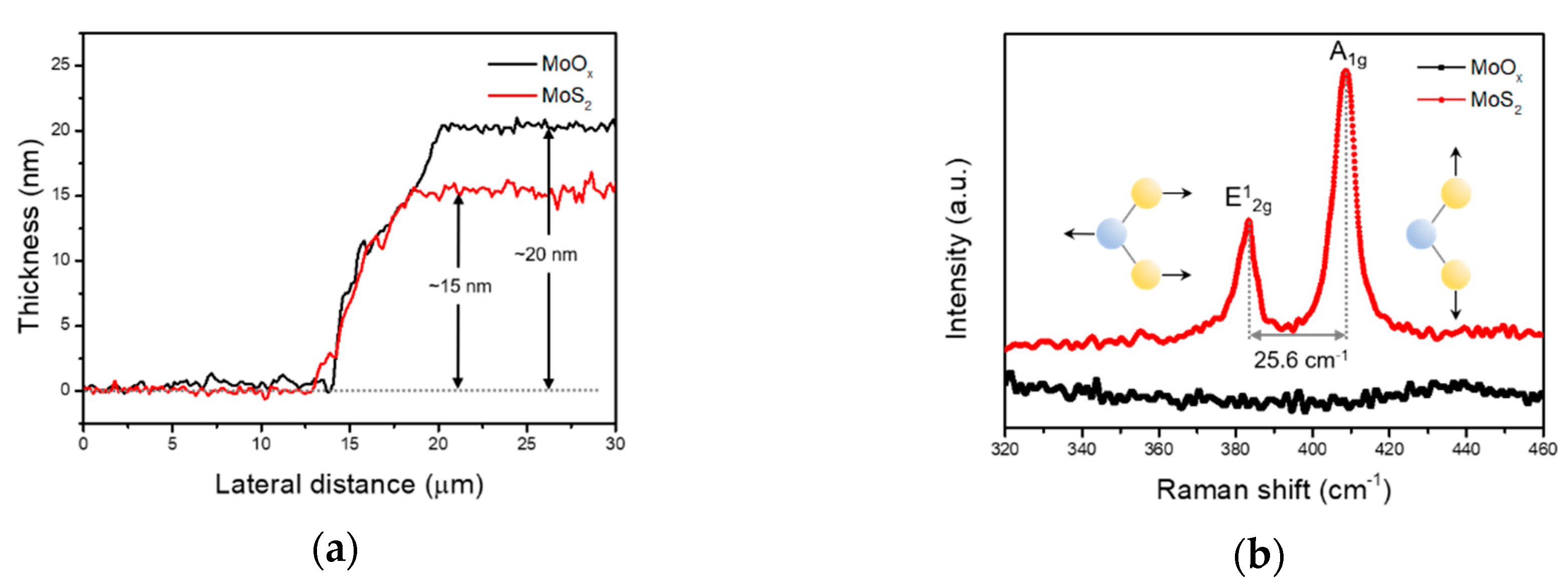
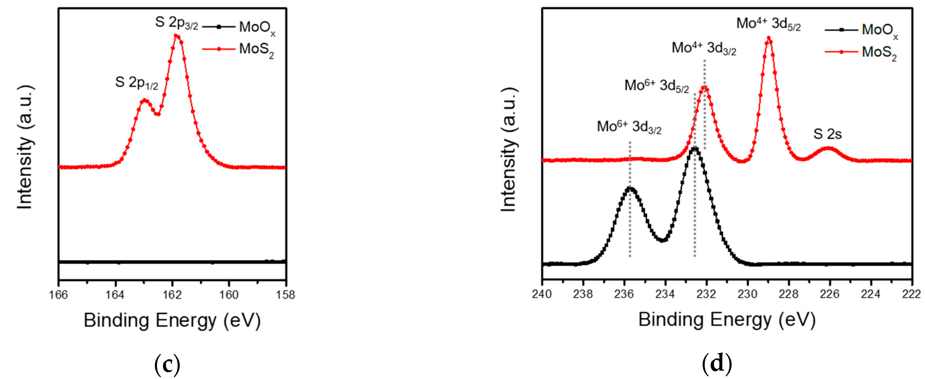
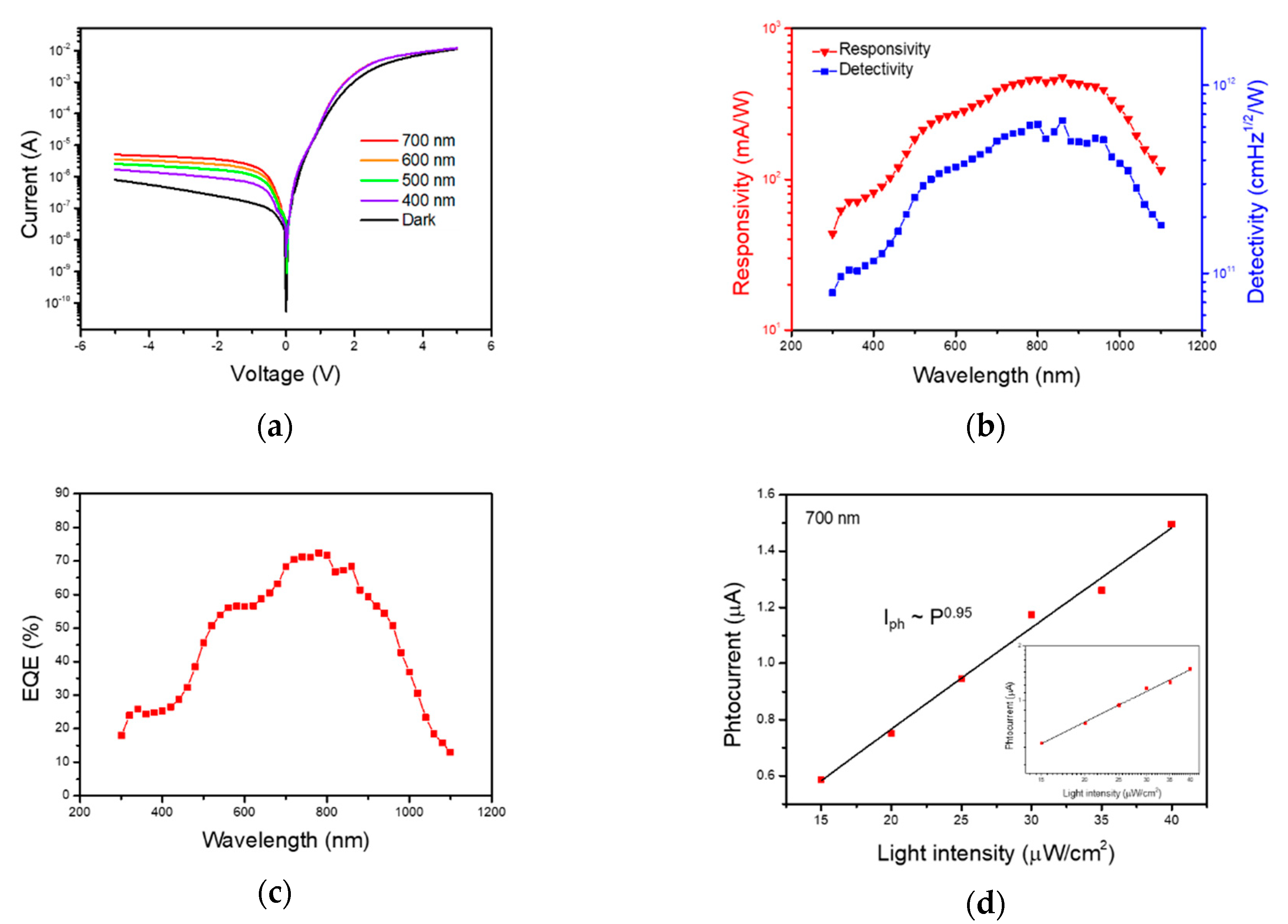
3. Results and Discussion

The MoS2 thin film was synthesized on upper side of the p-type silicon substrate by sulfurization process. The junction of the MoS2 film and p-type silicon substrate acts as a heterojunction diode consisting of two different semiconductors. The thickness profile measured by AFM is shown in Figure 1a. The thickness of MoOx film was confirmed 20 nm, while that of MoS2 film was 15 nm, corresponding to bulk MoS2. Figure 1b shows Raman spectroscopy of the MoOx and MoS2 films. Full range measurement is also shown in Figure S1. In case of MoOx film, any peaks of Raman spectra were not measured. Because MoOx film deposited by thermal evaporation is amorphous state [35]. While two typical phonon vibration modes were observed on the sulfurized MoS2 film, E12g and A1g phonon vibration mode. The E12g mode indicates an in-plane vibration of Mo and S atoms, whereas A1g mode represents an out-plane vibration, as shown in the inset of Figure 1b. Each of the phonon vibration modes is extracted at 382.7 cm−1 and 408.3 cm−1 by Gaussian curve fitting. The difference of the two phonon vibration modes is calculated to be 25.6 cm−1.
According to a previous report and AFM measurement of this work, it is confirmed that the MoS2 film is consistent with the bulk MoS2 [36]. Additionally, the sulfurized film shows good homogeneity from the Raman data in Figure S2 which is measured randomly at three points, two edges and one center parts. To verify the structure and crystallinity of the films, Raman spectroscopy and XRD measurement were performed on the p-type silicon substrates.
Figure 2a,b display the XRD data of MoOx and MoS2 films. The thermally evaporated MoOx film showed only silicon substrate peaks as reported previously [35]. This demonstrates that the MoOx film exists in an amorphous state without crystallinity. After sulfurization process, the MoS2 related XRD data clearly showed diffraction peaks indexed to (002), (100), (103), (006), (105), and (110) of hexagonal phase MoS2 (JCPDS No. 47-1492). It is clear that the sulfurized MoS2 film possesses high crystallinity. From the XRD data, average grain size was calculated to be about 10 nm using Scherrer equation as shown in Figure S3. XPS measurement was performed to analyze the chemical bonding of the MoOx and MoS2 films. Figure 2c shows the S 2p1/2 and S 2p3/2 peaks at 163.0 eV and 161.8 eV, respectively, of MoS2 film. No S peaks exist from MoOx film. Figure 2d displays the two distinct peaks for 3d electrons of the Mo atoms and one peak for 2s electrons of the S atoms. The MoOx film showed peaks for Mo6+ 3d3/2 and Mo6+ 3d5/2 at 235.7 eV and 232.6 eV, respectively. These peaks are consistent with those of MoO3. Additionally, no such peaks were observed related to S atoms. On the other hand, the sulfurized MoS2 film showed peaks at 232.1 eV, 229.0 eV and 226.1 eV which correspond to Mo4+ 3d3/2, Mo4+ 3d5/2 and S 2s, respectively. The XPS spectra results are consistent with those of the pristine sample. The O 1s core level and the atomic ratio are shown in Figure S4.
Figure 3a displays a schematic diagram of the n-MoS2/p-Si heterojunction diode. For Au/Ti/n-MoS2/p-Si/In structure, the current versus voltage (I-V) characteristics of the diode measured under dark conditions are shown in Figure 3b. The red line indicates the semi-log and the blue line indicates linear scale of I-V characteristics. The device showed clear rectifying behavior similar to that of p-n diodes. The reverse current was 8.0 × 10⁻⁷ A at −5 V and the forward current was 1.1 × 10⁻² A at 5 V. The rectification ratio of the diode was calculated to exceed 104, which is comparable to the previous report from our laboratory [32].
The I-V characteristics of the diode can be analyzed by using the following diode equation:
I = I 0 exp qV nkT 1
where I0 is the reverse bias saturation current, q is the electron charge, k is the Boltzmann’s constant, n is the ideality factor of the diode, and T is the absolute temperature. In the voltage range of V ≥ 4kT/q, the ‘−1’ term in the equation can be ignored. Therefore, the ideality factor of the heterojunction can be calculated by the following equation:
n = q kT dV d lnI
The ideality factor is an important value that provides an estimate of how closely the fabricated junction approaches the ideal diode situation. The ideality factor of the n-MoS2/p-Si diode was calculated to be 1.53, which indicates that the carrier transport phenomenon originated from both ideal diffusion process and recombination process. This value was calculated in the range of satisfying not only V ≥ 4kT/q mentioned previously, but also at low voltage enough to neglect series resistance and high injection effect. The recombination process may have originated from the existence of interface states of the n-MoS2/p-Si junction. Next, we further performed temperature dependent I-V measurements to calculate the effective barrier height of the diode. Figure 3c shows the temperature dependent I-V characteristics of the heterojunction. As the temperature decreases, the current value decreases. The barrier height can be determined by Richardson plot which is evaluated from thermionic emission theory of charge carriers:
ln I 0 T 2 = ln AA * q ϕ 0 k T
Here, A is the junction area (25 mm2) of the device, A* is the effective Richardson constant, ϕ0 is the barrier height of the device, k is Boltzmann’s constant, and T is the absolute temperature. This calculation was carried out in the temperature range of 200–320 K. From the Richardson plot as shown in Figure 3d, the barrier height of 0.27 eV was extracted for the n-MoS2/p-Si heterojunction.
From the energy band diagram in Figure 4, the band offset of the n-MoS2/p-Si diode is confirmed as a type Ⅱ heterojunction. The electron affinity and band gap of bulk MoS2 are 4.3 eV and 1.3 eV, respectively [37]. In the case of silicon, electron affinity and band gap are 4.05 eV and 1.12 eV, respectively. Due to the energy difference of Fermi levels, energy levels bend each other as the junction is formed. At the equilibrium state, the electrons in the n-type MoS2 lay er diffuse to the p-type silicon layer, while the holes in the p-type silicon diffuse to the n-type MoS2. A depletion layer is thereby created at the interface of n-MoS2/p-Si heterojunction.
A certain barrier height can be created, making it possible to show rectification characteristics. As the forward bias is applied, the barrier height and the depletion region decrease. Therefore, the carriers drift to each of the semiconductor layers. On the other hand, as the reverse bias is applied, the barrier height and the depletion region increase. The carriers cannot then drift to each of the semiconductor layers. Under illumination, electron-hole pairs will be generated and separated by the electric field in the depletion region and with applied bias. Photocurrent increases by the photo-generated carriers. On the reverse bias, the large electric field can serve to separate the photo-generated carriers and the photocurrent can be enhanced.
We further investigated the photo-response characteristics under light illumination. Figure 5a describes the I-V characteristics while varying the illumination wavelength from 400 nm to 700 nm at increments of 100 nm, with constant light intensity of 50 μW/cm2. At the forward bias region, only small current variation occurred compared with the dark condition. However, because of large electric field at the reverse bias region, a significant current difference appeared of about 10 times larger than the dark current. In this range, maximum photocurrent was generated around 700 nm. Furthermore, we measured the photo-response characteristics more precisely at a wide spectral range of wavelengths. The photoresponsivity represents the response capability of generated photocurrent per incident light, which is also called spectral responsivity.
The left axis of Figure 5b shows the photoresponsivity of the device at fixed reverse bias voltage of −5 V. It can be calculated from the following equation:
R = I ph P × A
Here, R is the photoresponsivity (A/W), P is the light intensity (W/cm2), A is the active junction area (25 mm2), Iph is photocurrent which can be calculated as Ilight-Idark (Ilight: current at light illumination, Idark: current at dark condition). The n-MoS2/p-Si heterojunction is confirmed as possessing broadband photoresponsivity at spectral range from about 300 nm to 1100 nm. The photoresponsivity increases with increasing wavelength to 860 nm, which corresponds to I-V characteristics under illumination. At longer wavelengths, photoresponsivity decreases. This tendency is like other previously reported results [14,37,38]. The maximum photoresponsivity of the n-MoS2/p-Si heterojunction shows 475 mA/W at 860 nm light. The photoresponsivity value of our n-MoS2/p-Si device is lower than that of mechanically exfoliated single crystal MoS2 based photodiode but comparable to previous reports [14,37].
Next, we evaluated the detectivity at reverse bias of −2 V. The detectivity describes the capacity for photo-detecting at weak optical power, which can be calculated using the following equation:
D * = A 1 / 2 R 2 qI dark 1 / 2
where D* is the detectivity. To show high detectivity, low dark current and high responsivity are needed. Based on the above equation, the detectivity is changed from 7.9 × 10¹⁰ Jones to 6.5 × 10¹¹ Jones as shown in right axis of Figure 5b. The maximum detectivity of 6.5 × 10¹¹ Jones is measured at the wavelength of 860 nm. Because of the low dark current at the reversed bias, which is a typical characteristic of junction type photodetectors, the calculated detectivity is much higher than phototransistors or photoconductors [39]. The external quantum efficiency (EQE) is defined as the number of photogenerated carriers produced per illuminated photons. This can be calculated by using the following equation:
EQE   % = electrons / s photons / s × 100 = I ph q h ν P opt × 100
Here, h is Planck’s constant, ν is the frequency of the light, and Popt is the optical power. An EQE value of 100% would show the ideal case in which one photon generated one electron-hole pair. Figure 5c shows the measured EQE of our device at reverse bias of −5 V. In our n-MoS2/p-Si device, the maximum EQE extracted was 72% at 780 nm wavelength.
We also extracted photo-response properties under various light intensities. The photocurrent was measured by varying the light intensity from 15 to 40 μW/cm2 at wavelength of 700 nm. The photocurrent data in Figure 5d and the inset display not a linear shape but rather a power-law fitting shape as a function of light intensity. It can be described by the following equation:
I ph = AP α
where A is a scaling constant, P is the light intensity, and α is an exponent determining factor. The exponent value is less than unity because of complex process of electron-hole generation, trapping, and recombination [37,38,40]. The exponent α of our n-MoS2/p-Si diode was calculated to be 0.95 at a reverse bias of −1 V, which means that the photocurrent value is close to the linear graph and the n-MoS2/p-Si diode has a remarkable capability for photodetection with a low density of defect trap states. Since silicon substrate is a perfect single crystal without defect, the defect trap states may originate from the MoS2 film. Previous paper reported the trap states of MoS2 films were sulfur vacancies and antisite defects [41]. Moreover, sulfur vacancies were observed in the sputtered film previously [42,43].
The light illumination response time is another key factor for fast light detecting application. We evaluated the response speed of the n-MoS2/p-Si diode as a photodetector at a fixed reverse bias voltage of −1 V under square-pulse light illumination with a 780 nm wavelength. Figure S5a shows the photocurrent transient characteristics for three cycles which are measured at 1 Hz by pulse generator. The results demonstrate excellent repeatability and stability. We calculated the response time and decay time of the n-MoS2/p-Si diode with exponential fitting. The rising part and decaying part are displayed in Figure S5b and Figure S5c, respectively. The rise time τr and the decay time τd were extracted to be 19.78 ms and 0.99 ms, respectively. These results are faster than silicon device which indicates that the photo-generated electron-hole pairs are effectively generated and separated by electric field and reverse bias of the junction interface. Our n-MoS2/p-Si device and the previously investigated MoS2- and Si-based photodetectors are compared in Table 1. Our device displays inferior photoresponsivity compared to the MoS2/p+-Si photodiode, which was fabricated via a mechanical exfoliation method in our lab. However, the detectivity of our device is higher, and the rise time and decay time are lower as well [32]. Furthermore, our photodiode showed superior responsivity to previously reported large-area satisfying devices.

4. Conclusions

In summary, n-MoS2/p-Si heterojunction was fabricated by sulfurization process of the MoOx film, which is thermally deposited on the p-type silicon substrate. Their electrical properties at room temperature typically showed the ideality factor of 1.53 and rectification ratio in excess of 104. Barrier height of 0.27 eV was obtained from the temperature dependent I-V characteristics. The heterojunction showed broadband photo-response performance with the maximum external quantum efficiency of 72% from visible to near-infrared range. The maximum photoresponsivity of 475 mA/W and detectivity of 6.5 × 10¹¹ Jones was obtained at the wavelength of 860 nm. From the transient properties, rise and decay times were extracted as 19.78 ms and 0.99 ms, respectively. This work shows the potential of sulfurization process for creation of large area MoS2 film and its heterojunction formation in highly efficient photovoltaic devices and other applications.

Supplementary Materials

The following are available online at https://www.mdpi.com/1424-8220/20/24/7340/s1, Figure S1: Raman spectroscopy of the MoOx and MoS2 films, Figure S2: Raman spectra of the sulfurized MoS2 films on three points, Figure S3: XRD data of the sulfurized MoS2 film, Figure S4: XPS data of O 1s core level from MoOx, sulfurized MoS2, and MoS2 bulk crystal, Figure S5: Photocurrent transient characteristics under square pulsed light illumination.

Author Contributions

Y.K. performed the experiment, analyzed the data, discussed the results and wrote the paper; T.K. discussed the results; and E.K.K. performed paper editing and supervision. All authors have read and agreed to the published version of the manuscript.

Funding

This work was supported in part by the National Research Foundation of Korea (NRF) grant funded by the Korean government (MSIP) (NRF-2020R1A4A4078674).

Conflicts of Interest

The authors declare no conflict of interest.

References

  1. Geim, A.K.; Novoselov, K.S. The rise of graphene. Nat. Mater. 2010, 6, 183–191. [Google Scholar] [CrossRef] [PubMed]
  2. Liu, L.; Shen, Z. Bandgap engineering of graphene: A density functional theory study. Appl. Phys. Lett. 2009, 95, 252104. [Google Scholar] [CrossRef]
  3. Meric, I.; Han, M.Y.; Young, A.F.; Ozyilmaz, B.; Kim, P.; Shepard, K.L. Current saturation in zero-bandgap, top-gated graphene field-effect transistors. Nat. Nanotechnol. 2008, 3, 654–659. [Google Scholar] [CrossRef] [PubMed]
  4. Podzorov, V.; Gershenson, M.E.; Kloc, C.; Zeis, R.; Bucher, E. High-mobility field-effect transistors based on transition metal dichalcogenides. Appl. Phys. Lett. 2004, 84, 3301–3303. [Google Scholar] [CrossRef] [Green Version]
  5. Chu, C.H.; Lin, H.C.; Yeh, C.H.; Liang, Z.Y.; Chou, M.Y.; Chiu, P.W. End-bonded metal contacts on WSe2 field-effect transistors. ACS Nano 2019, 13, 8146–8154. [Google Scholar] [CrossRef]
  6. Zhao, P.; Azcatl, A.; Bolshakov, P.; Moon, J.; Hinkle, C.L.; Hurley, P.K.; Wallace, R.M.; Young, C.D. Effects of annealing on top-gated MoS2 transistors with HfO2 dielectric. J. Vac. Sci. Technol. 2017, 35, 01A118. [Google Scholar] [CrossRef]
  7. Larentis, S.; Fallahazad, B.; Tutuc, E. Field-effect transistors and intrinsic mobility in ultra-thin MoSe2 layers. Appl. Phys. Lett. 2012, 101, 223104. [Google Scholar] [CrossRef] [Green Version]
  8. Yu, L.; Zubair, A.; Santos, E.J.; Zhang, X.; Lin, Y.; Zhang, Y.; Palacios, T. High-performance WSe2 complementary metal oxide semiconductor technology and integrated circuits. Nano Lett. 2015, 15, 4928–4934. [Google Scholar] [CrossRef] [Green Version]
  9. Tosun, M.; Chuang, S.; Fang, H.; Sachid, A.B.; Hettick, M.; Lin, Y.; Zeng, Y.; Javey, A. High-gain inverters based on WSe2 complementary field-effect transistors. ACS Nano 2014, 8, 4948–4953. [Google Scholar] [CrossRef]
  10. Lim, J.Y.; Pezeshki, A.; Oh, S.; Kim, J.S.; Lee, Y.T.; Yu, S.; Hwang, D.K.; Lee, G.H.; Choi, H.J.; Im, S. Homogeneous 2D MoTe2 p–n Junctions and CMOS Inverters formed by Atomic-Layer-Deposition-Induced Doping. Adv. Mater. 2017, 29, 1701798. [Google Scholar] [CrossRef]
  11. Wang, H.; Yu, L.; Lee, Y.H.; Shi, Y.; Hsu, A.; Chin, M.L.; Li, L.J.; Dubey, M.; Kong, J.; Palacios, T. Integrated circuits based on bilayer MoS2 transistors. Nano Lett. 2012, 12, 4674–4680. [Google Scholar] [CrossRef] [PubMed] [Green Version]
  12. Cheng, R.; Li, D.; Zhou, H.; Wang, C.; Yin, A.; Jiang, S.; Liu, Y.; Chen, Y.; Huang, Y.; Duan, X. Electroluminescence and photocurrent generation from atomically sharp WSe2/MoS2 heterojunction p–n diodes. Nano Lett. 2014, 14, 5590–5597. [Google Scholar] [CrossRef] [PubMed] [Green Version]
  13. Deng, Y.; Luo, Z.; Conrad, N.J.; Liu, H.; Gong, Y.; Najmaei, S.; Ajayan, P.M.; Lou, J.; Xu, X.; Ye, P.D. Black phosphorus–monolayer MoS2 van der Waals heterojunction p–n diode. ACS Nano 2014, 8, 8292–8299. [Google Scholar] [CrossRef] [PubMed] [Green Version]
  14. Desai, P.; Ranade, A.K.; Mahyavanshi, R.; Tanemura, M.; Kalita, G. Influence of MoS2-Silicon Interface States on Spectral Photoresponse Characteristics. Phys. Status Solidi 2019, 216, 1900349. [Google Scholar] [CrossRef]
  15. Chuang, S.; Battaglia, C.; Azcatl, A.; McDonnell, S.; Kang, J.S.; Yin, X.; Tosun, M.; Kapadia, R.; Fang, H.; Wallace, R.M.; et al. MoS2 p-type transistors and diodes enabled by high work function MoOx contacts. Nano Lett. 2014, 14, 1337–1342. [Google Scholar] [CrossRef] [Green Version]
  16. Chen, Y.; Wang, X.; Wu, G.; Wang, Z.; Fang, H.; Lin, T.; Sun, S.; Shen, H.; Hu, W.; Wang, J.; et al. High-performance photovoltaic detector based on MoTe2/MoS2 van der Waals heterostructure. Small 2018, 14, 1703293. [Google Scholar] [CrossRef]
  17. Dhyani, V.; Das, M.; Uddin, W.; Muduli, P.K.; Das, S. Self-powered room temperature broadband infrared photodetector based on MoSe2/germanium heterojunction with 35 A/W responsivity at 1550 nm. Appl. Phys. Lett. 2019, 114, 121101. [Google Scholar] [CrossRef]
  18. Wang, X.; Wang, P.; Wang, J.; Hu, W.; Zhou, X.; Guo, N.; Huang, H.; Sun, S.; Shen, H.; Lin, T.; et al. Ultrasensitive and broadband MoS2 photodetector driven by ferroelectrics. Adv. Mater. 2015, 27, 6575–6581. [Google Scholar] [CrossRef] [Green Version]
  19. Bertolazzi, S.; Krasnozhon, D.; Kis, A. Nonvolatile memory cells based on MoS2/graphene heterostructures. ACS Nano 2013, 7, 3246–3252. [Google Scholar] [CrossRef]
  20. Bessonov, A.A.; Kirikova, M.N.; Petukhov, D.I.; Allen, M.; Ryhänen, T.; Bailey, M.J. Layered memristive and memcapacitive switches for printable electronics. Nat. Mater. 2015, 14, 199–204. [Google Scholar] [CrossRef]
  21. Vu, Q.A.; Shin, Y.S.; Kim, Y.R.; Kang, W.T.; Kim, H.; Luong, D.H.; Lee, I.M.; Lee, K.; Ko, D.S.; Heo, S.; et al. Two-terminal floating-gate memory with van der Waals heterostructures for ultrahigh on/off ratio. Nat. Commun. 2016, 7, 1–8. [Google Scholar] [CrossRef] [PubMed]
  22. Lee, G.H.; Yu, Y.J.; Cui, X.; Petrone, N.; Lee, C.H.; Choi, M.S.; Lee, D.Y.; Lee, C.; Yoo, W.J.; Watanabe, K.; et al. Flexible and transparent MoS2 field-effect transistors on hexagonal boron nitride-graphene heterostructures. ACS Nano 2013, 7, 7931–7936. [Google Scholar] [CrossRef] [PubMed]
  23. Zheng, Z.; Zhang, T.; Yao, J.; Zhang, Y.; Xu, J.; Yang, G. Flexible, transparent and ultra-broadband photodetector based on large-area WSe2 film for wearable devices. Nanotechnology 2016, 27, 225501. [Google Scholar] [CrossRef] [PubMed]
  24. Nam, H.; Oh, B.R.; Chen, M.; Wi, S.; Li, D.; Kurabayashi, K.; Liang, X. Fabrication and comparison of MoS2 and WSe2 field-effect transistor biosensors. J. Vac. Sci. Technol. 2015, 33, 06FG01. [Google Scholar] [CrossRef]
  25. Pham, T.; Li, G.; Bekyarova, E.; Itkis, M.E.; Mulchandani, A. MoS2-based optoelectronic gas sensor with sub-parts-per-billion limit of NO2 gas detection. ACS Nano 2019, 13, 3196–3205. [Google Scholar] [CrossRef]
  26. Splendiani, A.; Sun, L.; Zhang, Y.; Li, T.; Kim, J.; Chim, C.Y.; Galli, G.; Wang, F. Emerging photoluminescence in monolayer MoS2. Nano Lett. 2010, 10, 1271–1275. [Google Scholar] [CrossRef]
  27. Bao, W.; Cai, X.; Kim, D.; Sridhara, K.; Fuhrer, M.S. High mobility ambipolar MoS2 field-effect transistors: Substrate and dielectric effects. Appl. Phys. Lett. 2013, 102, 042104. [Google Scholar] [CrossRef] [Green Version]
  28. Wu, W.; De, D.; Chang, S.C.; Wang, Y.; Peng, H.; Bao, J.; Pei, S.S. High mobility and high on/off ratio field-effect transistors based on chemical vapor deposited single-crystal MoS2 grains. Appl. Phys. Lett. 2013, 102, 142106. [Google Scholar] [CrossRef] [Green Version]
  29. Lee, H.S.; Ahn, J.; Shim, W.; Im, S.; Hwang, D.K. 2D WSe2/MoS2 van der Waals heterojunction photodiode for visible-near infrared broadband detection. Appl. Phys. Lett. 2018, 113, 163102. [Google Scholar] [CrossRef]
  30. Choi, M.S.; Qu, D.; Lee, D.; Liu, X.; Watanabe, K.; Taniguchi, T.; Yoo, W.J. Lateral MoS2 p–n junction formed by chemical doping for use in high-performance optoelectronics. ACS Nano 2014, 8, 9332–9340. [Google Scholar] [CrossRef]
  31. Choi, W.; Cho, M.Y.; Konar, A.; Lee, J.H.; Cha, G.B.; Hong, S.C.; Kim, S.; Kim, J.; Jena, D.; Joo, J.; et al. High-detectivity multilayer MoS2 phototransistors with spectral response from ultraviolet to infrared. Adv. Mater. 2012, 24, 5832–5836. [Google Scholar] [CrossRef] [PubMed]
  32. Song, D.Y.; Chu, D.; Lee, S.K.; Pak, S.W.; Kim, E.K. High photoresponsivity from multilayer MoS2/Si heterojunction diodes formed by vertically stacking. J. Appl. Phys. 2017, 122, 124505. [Google Scholar] [CrossRef]
  33. Huang, C.Y.; Chang, C.; Lu, G.Z.; Huang, W.C.; Huang, C.S.; Chen, M.L.; Lin, T.N.; Chen, J.L.; Lin, T.Y. Hybrid 2D/3D MoS2/GaN heterostructures for dual functional photoresponse. Appl. Phys. Lett. 2018, 112, 233106. [Google Scholar] [CrossRef]
  34. Shin, G.H.; Park, J.; Lee, K.J.; Lee, G.B.; Jeon, H.B.; Choi, Y.K.; Yu, K.; Choi, S.Y. Si–MoS2 Vertical Heterojunction for a Photodetector with High Responsivity and Low Noise Equivalent Power. ACS Appl. Mater. Interfaces 2019, 11, 7626–7634. [Google Scholar] [CrossRef]
  35. Battaglia, C.; Yin, X.; Zheng, M.; Sharp, I.D.; Chen, T.; McDonnell, S.; Azcatl, A.; Carraro, C.; Ma, B.; Maboudian, R.; et al. Hole selective MoOx contact for silicon solar cells. Nano Lett. 2014, 14, 967–971. [Google Scholar] [CrossRef]
  36. Li, H.; Zhang, Q.; Yap, C.C.R.; Tay, B.K.; Edwin, T.H.T.; Olivier, A.; Baillargeat, D. From bulk to monolayer MoS2: Evolution of Raman scattering. Adv. Funct. Mater. 2012, 22, 1385–1390. [Google Scholar] [CrossRef]
  37. Wang, L.; Jie, J.; Shao, Z.; Zhang, Q.; Zhang, X.; Wang, Y.; Sun, Z.; Lee, S.T. MoS2/Si heterojunction with vertically standing layered structure for ultrafast, high-detectivity, self-driven visible–near infrared photodetectors. Adv. Funct. Mater. 2015, 25, 2910–2919. [Google Scholar] [CrossRef]
  38. Zhang, Y.; Yu, Y.; Mi, L.; Wang, H.; Zhu, Z.; Wu, Q.; Zhang, Y.; Jiang, Y. In Situ Fabrication of Vertical Multilayered MoS2/Si Homotype Heterojunction for High-Speed Visible–Near-Infrared Photodetectors. Small 2016, 12, 1062–1071. [Google Scholar] [CrossRef]
  39. Huang, Z.; Zhang, T.; Liu, J.; Zhang, L.; Jin, Y.; Wang, J.; Jiang, K.; Fan, S.; Li, Q. Amorphous MoS2 Photodetector with Ultra-Broadband Response. ACS Appl. Electron. Mater. 2019, 1, 1314–1321. [Google Scholar] [CrossRef]
  40. Zeng, L.H.; Wang, M.Z.; Hu, H.; Nie, B.; Yu, Y.Q.; Wu, C.Y.; Wang, L.; Hu, J.G.; Xie, C.; Liang, F.X.; et al. Monolayer graphene/germanium Schottky junction as high-performance self-driven infrared light photodetector. ACS Appl. Mater. Interfaces 2013, 5, 9362–9366. [Google Scholar] [CrossRef]
  41. Hong, J.; Hu, Z.; Probert, M.; Li, K.; Lv, D.; Yang, X.; Gu, L.; Mao, N.; Feng, Q.; Xie, L.; et al. Exploring atomic defects in molybdenum disulphide monolayers. Nat. Commun. 2015, 6, 1–8. [Google Scholar] [CrossRef] [PubMed] [Green Version]
  42. Matsuura, K.; Ohashi, T.; Muneta, I.; Ishihara, S.; Kakushima, K.; Tsutsui, K.; Ogura, A.; Wakabayashi, H. Low-carrier-density sputtered MoS2 film by vapor-phase sulfurization. J. Electron. Mater. 2018, 47, 3497–3501. [Google Scholar] [CrossRef]
  43. Tongay, S.; Suh, J.; Ataca, C.; Fan, W.; Luce, A.; Kang, J.S.; Liu, J.; Ko, C.; Raghunathanan, R.; Zhou, J.; et al. Defects activated photoluminescence in two-dimensional semiconductors: Interplay between bound, charged and free excitons. Sci. Rep. 2013, 3, 1–5. [Google Scholar] [CrossRef] [PubMed] [Green Version]
Figure 1. (a) Thickness of the MoOx and MoS2 films measured by AFM are about 20 nm and 15 nm, respectively. (b) Comparison of the MoOx and MoS2 films from Raman spectroscopy. The sulfurized film shows two typical phonon modes, E12g and A1g, with peak difference of 25.6 cm−1.
Sensors 20 07340 g001
Figure 2. (a) (002)-Oriented XRD data, (b) (100), (103), (006), (105), and (110)-oriented XRD spectra. The gray-colored dash square indicates the substrate peaks. XPS spectra of Mo 3d (c) and S 2p (d) core levels of the MoOx and MoS2 films.
Sensors 20 07340 g002aSensors 20 07340 g002b
Figure 3. (a) Schematic diagram of the n-MoS2/p-Si heterojunction diode. The inset in (a) shows photograph of the heterojunction diode. (b) Electrical characterization of n-MoS2/p-Si heterojunction on semi-log scale (red) and linear scale (blue). (c) Temperature dependent I-V measurement in semi-log scale. (d) Richardson plot from the I-V measurement. The barrier height was calculated to be 0.27 eV.
Sensors 20 07340 g003
Figure 4. (a) p-type silicon and n-MoS2 energy band diagrams. (b) The energy band diagram of n-MoS2/p-Si heterojunction in equilibrium state.
Sensors 20 07340 g004
Figure 5. (a) I-V measurement comparison at the different visible wavelengths and light intensity of 50 μW/cm2. (b) Wavelength dependent responsivity, detectivity, and (c) EQE. (d) Light intensity versus photocurrent graph in linear scale and semi-log scale (inset).
Sensors 20 07340 g005
Table 1. Comparison of MoS2 and Si based photodetectors.
StructureMethodResponsivityDetectivity
[cm Hz1/2/W]
Rise/Decay TimeReference
MoS2/p-SiSulfurization475 mA/W6.5 × 101119.78/0.99 msThis work
MoS2/p+-SiMechanical exfoliation980 A/W~1090.2/2.1 s[32]
MoS2/p-SiSulfurization139 mA/WN/AN/A[14]
MoS2/p-SiSputtering~300 mA/W~10133/40 μs[37]
Publisher’s Note: MDPI stays neutral with regard to jurisdictional claims in published maps and institutional affiliations.

