Article

Polarization-Insensitive Waveguide Schottky Photodetectors Based on Mode Hybridization Effects in Asymmetric Plasmonic Waveguides

Wuhan National Laboratory for Optoelectronics, Huazhong University of Science and Technology, Wuhan 430074, China
*
Author to whom correspondence should be addressed.
Sensors 2020, 20(23), 6885; https://doi.org/10.3390/s20236885
Submission received: 27 October 2020 / Revised: 17 November 2020 / Accepted: 26 November 2020 / Published: 2 December 2020
(This article belongs to the Special Issue Optical and Photonic Sensors)

Abstract

:
Two types of configurations are theoretically proposed to achieve high responsivity polarization-insensitive waveguide Schottky photodetectors, i.e., a dual-layer structure for 1.55 µm and a single-layer structure for 2 µm wavelength band. Mode hybridization effects between quasi-TM modes and sab1 modes in plasmonic waveguides are first presented and further investigated under diverse metal types with different thicknesses in this work. By utilizing the mode hybridization effects between quasi-TE mode and aab0 mode, and also quasi-TM and sab1 mode in our proposed hybrid plasmonic waveguide, light absorption enhancement can be achieved under both TE and TM incidence within ultrathin and short metal stripes, thus resulting in a considerable responsivity for Si-based sub-bandgap photodetection. For 1.55 µm wavelength, the Au-6 nm-thick device can achieve absorptance of 99.6%/87.6% and responsivity of 138 mA·W−1/121.2 mA·W−1 under TE/TM incidence. Meanwhile, the Au-5 nm-thick device can achieve absorptance of 98.4%/90.2% and responsivity of 89 mA·W−1/81.7 mA·W−1 under TE/TM incidence in 2 µm wavelength band. The ultra-compact polarization-insensitive waveguide Schottky photodetectors may have promising applications in large scale all-Si photonic integrated circuits for high-speed optical communication.

1. Introduction

To meet the rising demands in optical communication, light detection and ranging (LiDAR), and nonlinear photonics, photodetectors (PDs) operating on 1.55 µm and beyond are highly desired. With the development of all-silicon integration, Si Schottky PDs based on internal photoemission (IPE) effect [1,2,3,4,5,6,7] have drawn much interest and been demonstrated in several platforms in recent decades. In such IPE-based devices, incident photons are usually absorbed by metals or silicides, and then hot carriers are produced by Landau damping [8]. The excited hot carriers are emitted through the Schottky barrier (ΦB) of the metal (or silicide)/Si interface, finally collected as photocurrent, thus achieving below-bandgap photodetection.
For IPE-based Schottky PDs, there exist three main crucial challenges, including low internal quantum efficiency (IQE), low absorption rate and weak polarization independence. Focusing on these bottlenecks, extensive studies have been carried out.
Low IQE is the main obstacle of all detectors based on the IPE effect [9]. Several solutions have been adopted to improve IQE. Some silicides with low work function to form low ΦB between silicide/Si interfaces, such as PtSi (with ΦB of 0.208 eV), have been widely used in imaging arrays [10]. However, because of their large areas and ultralow ΦB, silicide-based Schottky PDs usually suffer from a large dark current, hence stringent work conditions (such as cryogenic temperature) are required. In addition, mirror force effects [11], which are enabled by controlling the bias of Schottky PDs, are utilized to lower ΦB. Furthermore, surrounding or embedding metal structures [12,13] have also been implanted to make hot carriers reflect over multiple Schottky junction interfaces and emit to Si more easily. Moreover, it has been theoretically studied that IQE can be enhanced by introducing a surface roughness [14] of a few atomic layers for metals. In recent years, two-dimensional (2D) materials (graphene [15,16,17,18,19,20], MoS2 [21], black phosphorus [22,23]) have been involved in Si-based infrared PDs with superior performances comparable to commercial III–V compound and Ge-based devices. Up to date, ultrathin metals/silicides [10,24,25] are widely adopted to provide the excited hot electrons with more opportunities to emit when they bounce in the metal/dielectric interfaces.
As for the absorption efficiency improvement of Si-based Schottky PDs, several resonant structures, such as micro cavity [16,25,26,27,28,29,30], nano-antennas [31], and gratings [32,33], have been theoretically or experimentally demonstrated in some surface-illuminated devices. Micro-ring resonators [34,35,36] with high Q values are often reported to obtain narrowband absorptance enhancement for waveguide Schottky PDs. Except for the resonant structures, some of the bound modes propagating along metal/semiconductor interfaces [37,38,39,40], have been utilized in waveguide Schottky PDs. However, the ssb0 mode (0 order bound mode whose Ey components are symmetric with y and x axes) with a low mode power attenuation (MPA) and weak optical confinement ability usually induces a long absorption length [37,38], while the ultra-small field profile of the sab0 mode (0 order bound mode whose Ey components are symmetric with y and asymmetric with x axes) leaves a challenge for efficient coupling from pure photonic mode [39]. Aiming to overcome these drawbacks of bound modes, mode hybridization effects between the quasi-TE mode and aab0 mode in plasmonic two-core waveguide [41] have been first presented and developed to achieve a high absorption rate of 95.6% theoretically within 5 nm-thick and 2.2 µm-long Au film under TE incidence for 1.55 µm. A linear array of gradient Au nanobricks employed on Si nanowire waveguide induces an absorptance of 95% for TE polarization at 1.55 µm wavelength within 830 nm of device length in theory [42]. More recently, a plasmonic photodetector utilizing supermode hybridization [43] has been experimentally demonstrated with a responsivity of 82 mA/W when a 10 V bias was applied. However, among all of the waveguide Schottky PDs, the majority hold strong dependence on the polarization of incident light, therefore limiting their applications in large scale silicon photonic integrated circuits (PICs).
It is obvious that some surface-illuminated devices with geometric symmetry are intrinsically polarization-independent [31], such as 2D nanoantenna and nanohole-based PDs. Additionally, a Schottky PD consisting of 1D multilayer grating [32] has been proposed in theory, achieving a polarization-insensitive optical absorptance of 98% at 1470 nm with the assistance of guide mode resonance. As for waveguide Schottky PDs, plasmonic silicon ridge waveguides, in which a metal film covering both the top and the sidewall of Si waveguide [44,45] are employed to achieve low polarization dependence deviation over the wavelength range of 1.2–1.6 µm. Nevertheless, to the best of our knowledge, research works on polarization-insensitive waveguide Schottky PDs have been seldom reported [44,45] over these years.
In this work, two types of waveguide Schottky PD structures are put forward, respectively for polarization-insensitive photodetection in the 1.55 and 2 µm wavelength range. In Section 2, the basic performance formulas of Schottky PDs are given. In Section 3, mode hybridization effects in two waveguide structures are analyzed and utilized to achieve high absorptance in ultrathin metal films within short lengths for TE and TM polarization. Except for the mode hybridization effects between quasi-TE mode and aab0 mode (0 order bound mode whose Ey components are asymmetric with y and x axes) which have been stated in [41], mode hybridization effects between the quasi-TM mode and sab1 (1 order bound mode whose Ey components are symmetric with the y axis and asymmetric with x axis) mode are first presented in this work. By utilizing the hybrid quasi-TE-aab0 modes and hybrid quasi-TM-sab1 modes with modified waveguide structures, our devices can obtain considerable absorptance for the incidence of TE and TM polarization, respectively. Thus, by combining with a higher IQE owing to the adoption of ultrathin metal films, a favorable responsivity can be achieved. In addition, we also use the eigenmode expansion (EME) method to make a quantitative description of the mode hybridization and absorption process, thus proving the reliability and self-consistency of the simulation results. The theoretical results of the absorption rate and responsivity spectra show broad operation wavelength ranges for these two non-resonant structures. In Section 4, the influence of the waveguide width offset on the absorption spectrum and feasibility are briefly discussed. In Section 5, performance comparisons are made between the reported polarization-insensitive Schottky PDs and this work. Our structures can possess competitive responsivity and dark current characteristics simultaneously. In addition, our design ideas may have potential applications in ultra-compact polarization manipulation and detection devices for Si PICs.

2. Performance Formulas

The responsivity of a Schottky PD can be obtained by
  R e s = A η i q h ν
where A denotes the absorption rate, q is the elementary charge, h is the Planck constant and ν is the frequency of incident photons, ηi is IQE.
The IQE can be calculated by
η i = 1 h v Φ B h v P ( E 0 ) d E 0 ,
where , ΦB, E0, and P(E0) are incident photon energy, the Schottky barrier height, the initial energy of the hot carrier and the total emission probability from metal into a semiconductor when the excited hot carrier energy is in the range of ΦB to hν.
Based on the thin film single Schottky barrier model proposed by Scales [24] (which has been briefly descripted in Figure 1), P(E0) can be written as follows:
P ( E 0 ) = P 0 + ( 1 P 0 ) P 1 + ( 1 P 0 ) ( 1 P 1 ) P 2 + + P n k = 0 n 1 ( 1 P k ) ,
where n = L 2 t l n h v Φ B represents the maximum reflection trips until the energy of the hot carrier is reduced to ΦB, P k = 1 2 ( 1 Φ B E k ) is the emission probability over a single Schottky barrier while the excess energy of a hot carrier is Ek. After k rounds of reflection within a metal thickness of t and carrier attenuation length of L, the excess energy Ek can be represented as E k = E 0 e 2 k t / L .
The dark current of Schottky PDs is closely related to the electric contact area (S) and ΦB. In Equation (4), A** is the effective Richardson constant (A** = 32 A cm−2K−2 for holes in Si), and kB is the Boltzmann constant, T is the absolute temperature (300 K in this work):
I d a r k = S A * * T 2 e q Φ B / k B T
The polarization dependent deviations (PDD) [44] can be obtained by
PDD = | R T E R T M | ( R T E + R T M ) / 2 × 100 % ,
where RTE and RTM denote responsivity under TE and TM incidence, respectively.
The normalized photocurrent to dark current ratio (NPDR) [46], which is a figure of merit to evaluate the detection ability, is represented as
NPDR = R e s I d a r k

3. Design Principle and Simulation Results

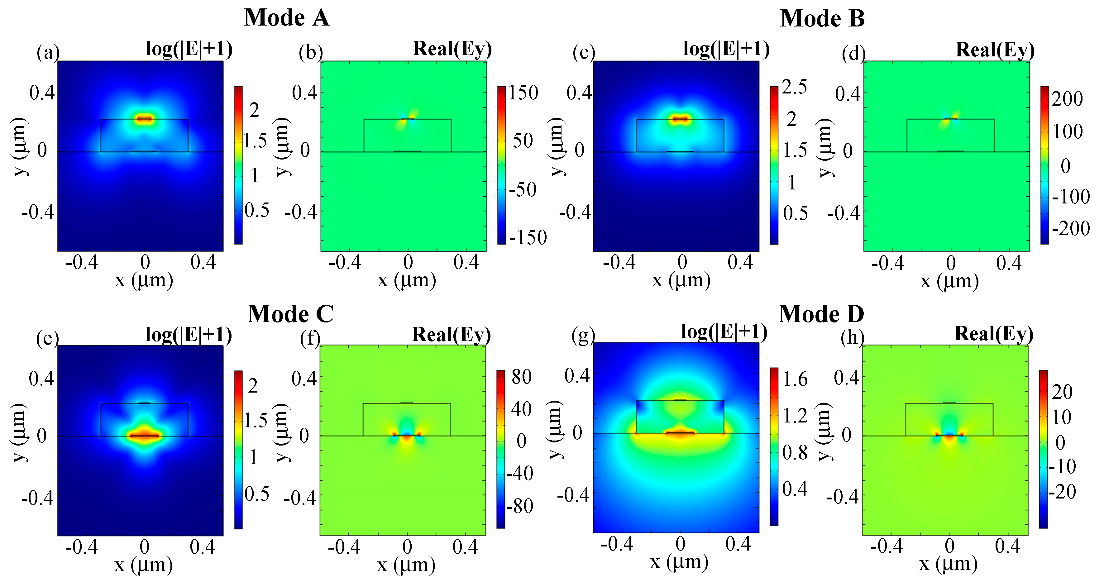
3.1. Dual-Layer Structure for 1.55 µm Operation

In Figure 2, a hybrid photonic–plasmonic waveguide, which consists of a Si nanowire waveguide and two layers of ultrathin metal with a thickness of hm (one embedded in a Si nanowire waveguide and the other laid upwards to the Si waveguide), is schematically shown. The width and height of Si nanowire waveguide are fixed at 600 and 220 nm, marked as wsi and hsi, respectively. The metal stripes are both composed of two slowly varying tapers and a rectangular section.
Owing to the complex structure of the three-core waveguide shown in Figure 2, we can make a simple classification of the modes into three categories, i.e., quasi-photonic modes with similar counterparts as photonic modes, bound modes which have a stronger electric field near the ‘top’ (‘t’) and ‘bottom’ (‘b’) metals, respectively. The following letters ‘s’ and ’a’ respectively refer to the ‘symmetry’ and ‘asymmetry’, which describe the symmetrical features of Ey components with respect to y and x axes [39]. The subscripted ‘b’ represents the ‘bound’ and the superscripted number is the order of the bound mode. The mode characteristics of the plasmonic waveguide were investigated by finite difference eigenmode (FDE) solver [47] (from Mode solutions software). In the preliminary study, wt was found to have significant influence on quasi-TE modes and t-bound modes, while wb seems to significantly influence the effective indices of quasi-TM and b-bound modes. As such, we display the effective indices of quasi-TE mode and t-bound modes together with the varying value of wt (at a fixed wb), and quasi-TM mode together with b-bound modes with the varying of wb (at a fixed wt), respectively. The real and imaginary parts of mode’s effective indices as wt (wb) increases from 0.01–0.35 µm with a fixed value of wb (wt) under different metal film thicknesses are shown in Figure 3.
Mode hybridization effects [48,49,50] have been studied thoroughly among various Si waveguides with asymmetry in vertical direction over the past decade. As shown in Figure 3, there also exists a mode hybridization effect between the quasi-TE and taab0 mode, as circled out by the red lines, which is consistent with what has been clarified in [41]. Significantly, mode hybridization effects between quasi-TM modes and bsab1 modes (marked with black circles) also exist in Figure 3. In the mode hybridization regions, the imaginary parts of the effective indices for quasi-photonic modes have a significant increase, and usually the electric field of two hybrid modes are too similar to distinguish. In comparison of Figure 3b with Figure 3f, with the increase in hm, both the real parts and imaginary parts of effective indices for bound modes reduce. Moreover, the mode hybridization region “shifts” to wider metal width, and a stronger interaction occurs between the two hybrid modes, which means that the mode conversions from quasi-photonic modes to bound modes may be easier with the increase in hm. It should be noticed that a larger hm leads to a sharp deterioration of IQE [24], so a compromise consideration is required when choosing hm. Moreover, it needs to be emphasized that in plasmonic waveguide with a single-layer metal film on the top of the Si waveguide, the mode hybridization effects between quasi-TM and sab1 mode also exist, but the MPA of quasi-TM mode in the mode hybridization region is not ideal in our waveguide settings (wSi = 600 nm, hSi = 220 nm) to achieve high absorbance within a few micrometers. Thus, we attempted to insert another metal layer on the top of SiO2 to improve the MPA of the quasi-TM mode in the mode hybridization region, which have been proven helpful for the promotion of absorption under TM incidence.
In addition, a steeper rise and larger extremum of MPA for quasi-photonic mode in the mode hybridization area can be realized with a smaller hm. While, in contrast, the MPA of quasi-photonic mode outside the mode hybridization region becomes larger as hm increases (see Figure 3b,f,d,h). Particularly, quasi-TM mode is cut-off after the mode hybridization area when hm increases to some extent, as shown in Figure 3g,h,k,l.
The electric field profiles of modes A, B, and modes C, D in the dual-layer plasmonic waveguide are shown in Figure 4. Modes A and B denote the modes with a higher and lower real part of the effective index between quasi-TE and taab0 mode, respectively. Similarly, Mode C represents the mode which holds a higher real part of the effective index between quasi-TM and bsab1 mode, while mode D represents the one with the lower real part. It can be seen from Figure 4 that the electric components are comparable between modes A and B, as well as modes C and D. The Ey components of modes A and B are asymmetric with respect to both the x and y axes (similar to aab0 mode). The Ey components of mode C and D are asymmetric with respect to x axis, while symmetric with respect to y axis (just like sab1 mode).
Inspired by the above mode analyses, a dual-layer modified taper was proposed to achieve high efficiency polarization-insensitive absorption in ultrathin and ultra-compact metal films. The operating principle of our proposed device is schematically depicted in Figure 5a. TE mode converts to quasi-TE mode without decoupling to a pure Si waveguide, with a slowly varying taper in length of lt1. Then, the quasi-TE mode converts to quasi-TE- taab0 hybrid modes in a modified second taper with a specific power ratio, which is similar to [41]. The mode conversion process of TM incidence is nearly the same as that of TE incidence. As marked by red lines, the TM mode is converted to quasi-TM mode in the first taper, coupled to quasi-TM-bsab1 hybrid modes in the second taper, and finally absorbed efficiently in the following rectangular segment.
To make a quantitative understanding of the mode evolution process, the eigenmode expansion (EME) methods are employed to describe the power transformation between the hybrid modes we were concerned about. We also made a comparison of the finite difference time domain (FDTD) method and the EME evaluation which is deduced by Equation (7), in which Ataper is the absorption rate in the first two tapers, and Am denotes the power coupled to mth modes at the end of the taper section (z = 0), nmi is the imaginary part of the mth mode effective refractive index, k0 is the wave vector and z is the position in the rectangular regions along the mode propagation direction (z axis):
A E M E = A t a p e r + m A m ( 1 e 2 n m i k 0 z )
By the separated EME monitors and “power absorbed” analysis groups in the FDTD solutions software [47], the power coupled to each mode and the cumulative absorption rates at several evenly spaced z points along the propagation direction can be acquired easily. As plotted in Figure 5b,c, the EME evaluated results (solid lines) are nearly the same as the FDTD-derived discrete absorption rates (dotted lines), and the power percentage decrement of the hybrid modes along the z axis is offset by the increment of absorption rate, indicating that there are ultralow scattering loss and reflection loss, simultaneously. The results from Figure 5b,c also confirm the self-consistency and credibility of our simulations. In addition, it can be found in Figure 5c that the power in mode B and mode A are both significant after the mode conversion section in the Au-12 nm-thick case. While, the power remains mostly in mode D (quasi-TM mode in Au-6 nm-thick case) in Figure 5b, which verifies the previous statement that mode conversion between two hybrid modes is much easier when hm is larger.
In addition, dual-layer metal configurations employing various metal types and thicknesses are simulated by the 3D-FDTD method [47] (from FDTD solutions software). The corresponding optimized geometric parameters and performances are tabulated in Table 1. The theoretical responsivity of the Au-6 nm-thick configuration is ~0.12 A/W, which is an appreciable value among traditional IPE-type Schottky PDs. Owing to the high ΦB between the Al and p-Si (as high as 0.58 eV), the IQEs of Al-based Schottky PDs are relatively limited and the responsivity is much lower than that of Au/p-Si-based devices (ΦB = 0.34 eV). In contrast, also due to their high ΦB, Al-based devices have an ultralow dark current (~0.01 nA), which is three orders of magnitude lower than that of Au-based devices at least.
The absorption rate and corresponding responsivity spectra of the dual-layer type Schottky PD (with an Au thickness of 6 nm) are also calculated (Figure 6a,b). Owing to the large MPA of quasi-TE mode (see in Figure 6c) and long absorption length ls, the ATE (absorption rates under TE incidence) can be maintained at nearly 100% within a wide wavelength range. While the ATM curve fits well with the power loss of pure quasi-TM mode within the propagation length of ls (shown in the inset of Figure 6a), proving that quasi-TM mode hardly converts to bsab1 mode in the whole propagation process. The MPA of quasi-TM mode reduces significantly when λ > 1.55 µm (see the inset of Figure 6d), so ATM degrades as expected. Nevertheless, responsivity in the wavelength range from 1.45 to 1.65 µm is higher than 40 mA/W, which shows an improvement for most traditional Schottky PDs.

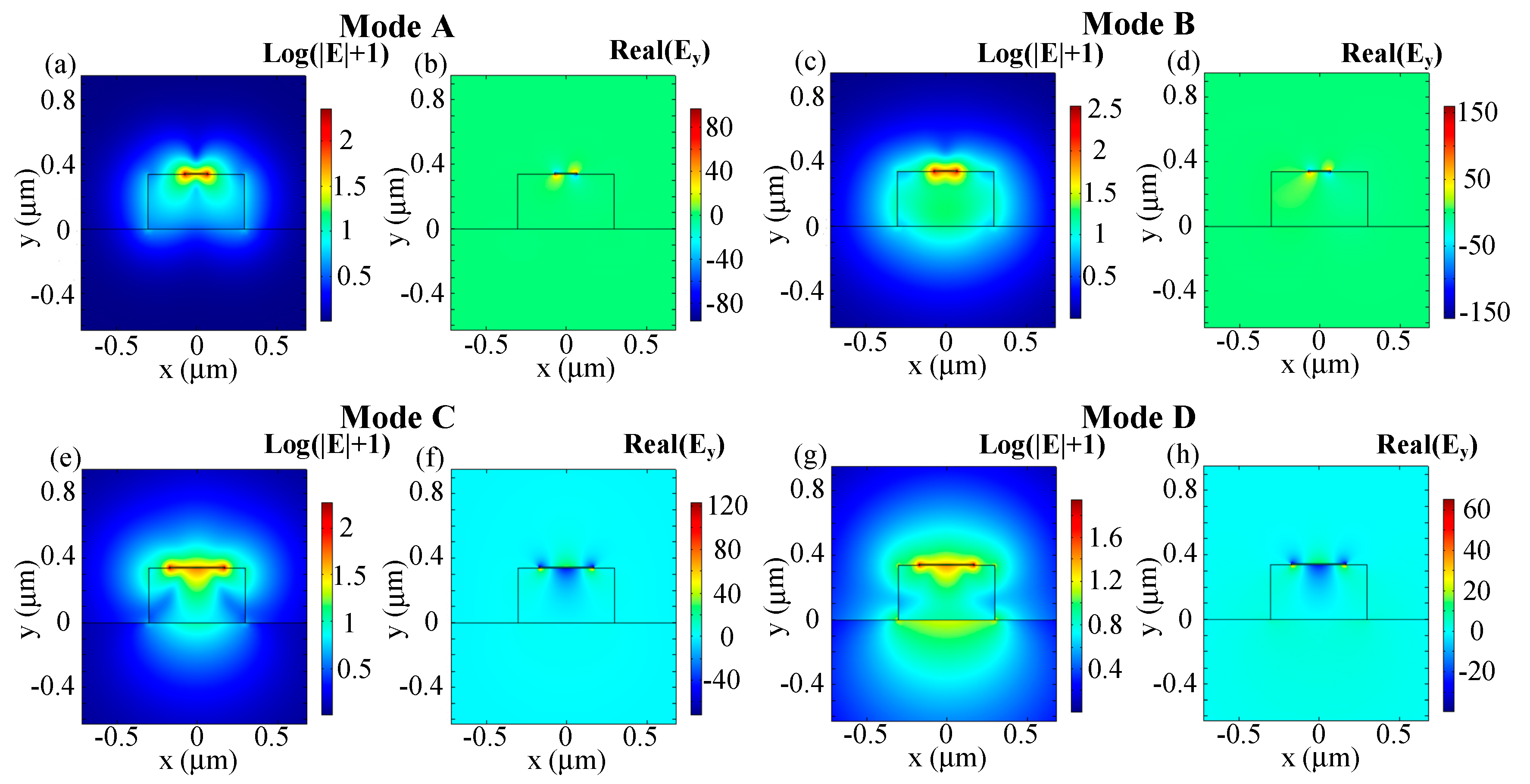
3.2. Single-Layer Structure for 2 µm Operation

Other than the above dual-layer structure, a modified single-layer metal stripe integrated with a Si nanowire waveguide is also developed to achieve polarization-insensitive sub-gap photodetection at a 2 µm wavelength band, as shown in Figure 7.
Figure 8 shows the effective indices of the modes supported by the plasmonic waveguide as wt increases from 0 to 0.6 µm when diverse metal types and thicknesses (respectively Au-5 nm for (a) (b), Au-7 nm for (c) (d), Al-2 nm for (e) (f), and Al-4 nm for (g) (h)) are applied. In the two-core plasmonic waveguides, mode hybridization effects also exist between quasi-TM mode and sab1 mode, as well as quasi-TE and aab0 mode. The mode hybridization areas are circled out by red and black circles, respectively. In these two areas, the imaginary parts of the effective indices for quasi-photonic modes increase significantly, and then reduce. In comparison with Figure 8b,d,f,h, it can be inferred that the “interaction” between quasi-photonic modes and corresponding hybridized bound modes are stronger as hm increases, while both the real and imaginary parts of bound modes decrease. Moreover, the imaginary part curve of the quasi-photonic mode exhibits a smaller peak value in the mode hybridization region as hm increases. In the Al-4 nm case presented in Figure 8g,h, it should be noted that quasi-TM modes also turn to be “cut-off” in the posterior segment of mode hybridization regions (similar to what has been shown in Section 3.1).
In order to describe the mode hybridization between quasi-TE and aab0 modes, as well as quasi-TM and sab1 modes more intuitively, the normalized electric fields and vertical components of the corresponding hybridized modes (when hm of Au film is 7 nm) are plotted in Figure 9. The naming rule is identical to that employed in Section 3.1. Comparable electric field components are demonstrated between mode A and mode B when wt = 0.14 µm, and also between mode C and mode D when wt = 0.34 µm. The high resemblance of the electric field components between the hybridized modes reconfirm the existence of mode hybridization effects in the plasmonic waveguide structure. Similar to bound modes, quasi-photonic modes also hold larger electric field intensity along the metal edges and large MPA within the mode hybridization regions.
Based on the mode analyses above, a multi-segment metal structure was put forward to achieve polarization-insensitive efficient absorption via an ultrathin metal stripe within a short device length, as shown in Figure 7. The operation principle (see also Figure 10a) is summarized as follows: for TE incidence, TE mode converts to quasi-TE mode along the first taper while wt1 is away from the mode hybridization area, and it may couple to hybrid modes with high MPAs in the second taper (with the length of lt2), in which mode hybridization between quasi-TE mode and aab0 mode exists, and finally achieve high absorptance during the propagation length of ls1. When it comes to TM incidence, quasi-TM modes are propagated and slowly weakened until the width increases to wt3, and coupled to quasi-TM-sab1 hybrid modes with a large MPA in the following part, eventually attenuated in the rectangular section with a length of ls2. Note that if the MPA of quasi-photonic modes under mode hybridization conditions are satisfactory enough, it is not necessary to achieve rigorous mode conversion from quasi-photonic modes to their corresponding hybridized bound modes for the purpose of absorptance promotion.
To ascertain the reliability of our simulations, the similar fitting methods which were introduced in Section 3.1 were used. The only difference is that the monitors are set in the rectangular segments with the length of ls1 and ls2 for TE and TM incidence, respectively. As plotted in Figure 10b,c, except for the optical power that has been absorbed, almost total residual power remains in quasi-photonic modes after the taper which functions as the mode conversion section, indicating that there is no significant mode conversion, owing to the relatively weak hybridization effects when extremely thin metal films (Au-5 nm and Al-2 nm in the above examples) are adopted.
Besides, the geometric parameters in the conditions of various metal types and thicknesses are optimized through 3D-FDTD numerical simulations, and the corresponding performances are also estimated. As summarized in Table 2, here the estimated responsivity for Au-based Schottky PDs is of 70~89 mA/W at a 2 µm wavelength band. Due to the obvious deterioration of IQE caused by the high Schottky barrier between Al and p-Si, the theoretical responsivity of Al-based devices at 2 µm is decreased by a factor of 20 compared with the result for 1.55 µm.
In Figure 11a,b, the absorption and responsivity spectra (Au-7 nm-thick device) in the wavelength range of 1.8–2.2 µm are plotted. The absorption rates under TE incidence (ATE) are almost above 80%. Due to the relatively high MPA of quasi-TE mode (see in Figure 11c) the ATE is expected to be improved by increasing ls1. As shown in Figure 11d, the MPA of the quasi-TM mode starts to decrease when λ > 2 µm. Moreover, the sab1 mode and quasi-TM mode are respectively cut-off at 2.01 and 2.1 µm when wt = wt4 = 0.338 µm (as 7 nm-thick Au film is adopted), so the absorption rates (in Figure 11a) for TM incidence fall drastically at a wavelength above 2 µm under our geometric settings. However, the structure exhibits a broad operation wavelength range over 300 nm (full width at half-maximum of the Res spectra in Figure 11b, here the Res greater than 40 mA/W are taken into account).

4. Discussions about Fabrication Tolerance and Feasibility

In order to study the influences of fabrication error on the absorption efficiency, we performed a further simulation with the offsets of metal width (+/-10 nm) and Si waveguide width (+/-50 nm) for an Au-7 nm-thick single layer structure. As shown in Figure 12a, a +10 nm offset of metal width could result in a 100 nm red shift of the TE absorption spectrum curve. However, for TM incidence, the red shift of the absorption spectrum is less significant than that of TE incidence.
When the Si waveguide width offsets are +/-50 nm, the absorption spectra of our proposed structure are almost the same as that of original structure parameters for TE incidence (in Figure 12b). For TM incidence, the offset of the Si waveguide width would lead to a change of cutoff wavelength for the quasi-TM mode. The quasi-TM mode would be cut off at a shorter wavelength when wSi is smaller, so the absorption spectrum would drop dramatically at a shorter wavelength when a narrower Si waveguide is applied. In general, the precise control of the metal film width is very crucial, which sets a challenge for the accuracy of the pattern transfer and etch procedures.
Up to now, the ultrathin metal films (5–7 nm) with good uniformity on dielectric surfaces are extremely hard to be realized in actual fabrication. However, there have been some progresses by utilizing molecular self-assembled monolayers [51] or 2D materials [52] as adhesion layers to improve the surface wetting of the metal on the dielectric. The sputtering method [51] and chemical vapor deposition [52] are used for the growth of ultrathin metal films with good uniformity and smoothness. However, the insertion of adhesion layers would somewhat modify the Schottky interface quality. Recently, an amorphous-Si Schottky photodetector [43] has been experimentally demonstrated. The 10 nm-thick Al film is deposited by electron beam evaporator (EBE) on the surface of SiO2 with a surface roughness of 1.49 nm. An impressive responsivity of 80 mA/W (under 10 V bias) has been achieved in the experiment. Given the recent progresses, our proposed devices may be implanted in actual fabrication with the assistance of advanced manufacturing technology in the near future.

5. Summary and Future Work

In this paper, we elaborated the existing problems in the research field of Si-based Schottky PDs. By studying the mode characteristic of multi-core plasmonic waveguide, the mode hybridization effects between quasi-TM mode and sab1 mode are first presented, as far as we know. By utilizing the hybridized quasi-TE-aab0 modes, hybridized quasi-TM-sab1 modes through the modified tapered metal stripes simultaneously, light absorption enhancement in ultrathin metal films are achieved within short lengths (<10 µm) under both TE and TM incidence. In a dual-layer metal structure for 1.55 µm, the absorption rate of 99.6%/87.6% and responsivity of 138 mA∙W−1/121.2 mA∙W−1 are achieved for TE/TM incidence within 6 nm-thick and 6.7 µm-long Au stripes, resulting in a PDD of 12.96%. As for the single-layer metal structure for 2 µm operation, the absorption rate of 98.4%/90.2% and responsivity of 89 mA∙W−1/81.7 mA∙W−1 are achieved under TE/TM polarization incidence within 5 nm-thick and 8.2 µm-long Au stripes in theory, with a PDD of 8.5%. We also give detailed studies of the mode characteristics and obtain optimized geometric parameters based on two configurations under diverse metal types and thicknesses.
In addition, we make comparisons between some previous works on polarization-insensitive Schottky detectors and this work. Geometric parameters and device performances are listed in Table 3. Our proposal holds better responsivity owing to enhanced absorptance (~90%) resulting from mode hybridization effects and moderate IQE attributed to the adoption of ultrathin metals. Moreover, the dark currents of Au-based and Al-based devices in this work are maintained at ~100 and ~0.01 nA (under low bias), respectively. However, it should be addressed that the PDDs of our designs are not as satisfactory as expected. Actually, by reducing the ATE through adjusting the metal widths artificially, an ultralow PDD also can be achieved at the expense of the RTE. The main contribution of this work is the observation of mode hybridization effects between quasi-photonic modes and bound modes, so only the absorption rates near the maximum under each incident polarization state are considered during the optimization processes. Meanwhile, there are relatively wide spectrum response ranges for the two types of our proposed structures, compared to some previously reported resonant-enhanced structures. We argue that the designs may have promising applications in high-density silicon PICs in the future.
Furthermore, based on the novel mode hybridization effects between quasi-photonic modes and bound modes, polarization-selective photodetection also can be flexibly realized by properly tailoring geometries, which may contribute to the detection of polarization characteristics in Si on-chip integrated circuits. In addition, the mode analyses of plasmonic waveguides may suggest the development of ultra-compact plasmonic polarization control devices, such as TE/TM-pass polarizers and polarization splitters.
Moreover, it needs to be emphasized that the theoretical responsivity in this work is inferior to the traditional photodiode based on the III–V compound or Ge/GeSn materials due to the limited IQE. To further increase the responsivity of the Schottky PDs, two-dimensional materials (such as graphene [53], MoS2) and multi-Schottky barrier structures are anticipated to be utilized, thus the extraction possibility of hot electrons will be boosted enormously.

Author Contributions

Q.L. performed simulations, J.T., Y.T. and Y.Z. contributed to the refinement of the article. All authors have read and agreed to the published version of the manuscript.

Funding

This research was funded by Chinese National Major Research and Development Program, grant number 2018YFB2200204.

Conflicts of Interest

The authors declare no conflict of interest.

References

  1. Goykhman, I.; Desiatov, B.; Khurgin, J.; Shappir, J.; Levy, U. Waveguide based compact silicon Schottky photodetector with enhanced responsivity in the telecom spectral band. Opt. Express 2012, 20, 28594–28602. [Google Scholar] [CrossRef] [PubMed]
  2. Casalino, M.; Coppola, G.; la Rue, R.M.; Logan, D.F. State of the art all silicon sub-bandgap photodetectors at telecom and datacom wavelengths. Laser Photonics Rev. 2016, 10, 895–921. [Google Scholar] [CrossRef] [Green Version]
  3. Muehlbrandt, S.; Melikyan, A.; Harter, T.; Köhnle, K.; Muslija, A.; Vincze, P.; Wolf, S.; Jakobs, P.; Fedoryshyn, Y.; Freude, W.; et al. Silicon-plasmonic internal-photoemission detector for 40 Gbit/s data reception. Optica 2016, 3, 741. [Google Scholar] [CrossRef]
  4. Desiatov, B.; Goykhman, I.; Mazurski, N.; Shappir, J.; Khurgin, J.B.; Levy, U. Plasmonic enhanced silicon pyramids for internal photoemission Schottky detectors in the near-infrared regime. Optica 2015, 2, 335–338. [Google Scholar] [CrossRef] [Green Version]
  5. Su, Y.; Lin, C.; Chang, P.; Helmy, A.S. Highly sensitive wavelength-scale amorphous hybrid plasmonic detectors. Optica 2017, 4, 1259–1262. [Google Scholar] [CrossRef] [Green Version]
  6. Gosciniak, J.; Atar, F.B.; Corbett, B.; Rasras, M. CMOS-Compatible Titanium Nitride for On-Chip Plasmonic Schottky Photodetectors. ACS Omega 2019, 4, 17223–17229. [Google Scholar] [CrossRef]
  7. Frydendahl, C.; Grajower, M.; Bar-David, J.; Zektzer, R.; Mazurski, N.; Shappir, J.; Levy, U. Giant enhancement of silicon plasmonic shortwave infrared photodetection using nanoscale self-organized metallic films. Optica 2020, 7, 371–379. [Google Scholar] [CrossRef] [Green Version]
  8. Brown, A.M.; Sundararaman, R.; Narang, P.; Goddard, W.A.; Atwater, H.A. Nonradiative Plasmon Decay and Hot Carrier Dynamics: Effects of Phonons, Surfaces, and Geometry. ACS Nano 2016, 10, 957. [Google Scholar] [CrossRef]
  9. Khurgin, J.B. Fundamental limits of hot carrier injection from metal in nanoplasmonics. Nanophotonics 2020, 9, 453–471. [Google Scholar] [CrossRef]
  10. Kosonocky, W.F.; Shallcross, F.V.; Villani, T.S.; Groppe, J.V. 160 × 244 Element PtSi Schottky-barrier IRCCD image sensor. IEEE Trans. Electron. Dev. 1985, 32, 1564–1573. [Google Scholar] [CrossRef]
  11. Sze, S.M.; Coleman, D.J., Jr.; Loya, A. Current transport in metal-semiconductor-metal (MSM) structures. Solid State Electron. 1971, 14, 1209–1218. [Google Scholar] [CrossRef]
  12. Knight, M.W.; Wang, Y.; Urban, A.S.; Sobhani, A.; Zheng, B.Y.; Nordlander, P.; Halas, N.J. Embedding plasmonic nanostructure diodes enhances hot electron emission. Nano Lett. 2013, 13, 1687–1692. [Google Scholar] [CrossRef]
  13. Fathauer, R.W.; Iannelli, J.M.; Nieh, C.W.; Hashimoto, S. Infrared response from metallic particles embedded in a single-crystal Si matrix: The layered internal photoemission sensor. Appl. Phys. Lett. 1990, 57, 1419–1421. [Google Scholar] [CrossRef]
  14. Grajower, M.; Levy, U.; Khurgin, J.B. The role of surface roughness in plasmonic-assisted internal photoemission schottky photodetectors. ACS Photonics 2018, 5, 4030–4036. [Google Scholar] [CrossRef]
  15. Casalino, M.; Sassi, U.; Goykhman, I.; Eiden, A.; Lidorikis, E.; Milana, S.; de Fazio, D.; Tomarchio, F.; Iodice, M.; Coppola, G.; et al. Vertically illuminated, resonant cavity enhanced, graphene–silicon Schottky photodetectors. ACS Nano 2017, 11, 10955–10963. [Google Scholar] [CrossRef] [PubMed] [Green Version]
  16. Casalino, M. Design of Resonant Cavity-Enhanced Schottky Graphene/Silicon Photodetectors at 1550 nm. J. Lightwave Technol. 2018, 36, 1766–1774. [Google Scholar] [CrossRef]
  17. Casalino, M.; Russo, R.; Russo, C.; Ciajolo, A.; di Gennaro, E.; Iodice, M.; Coppola, G. Free-Space Schottky Graphene/Silicon Photodetectors Operating at 2 μm. ACS Photonics 2018, 5, 4577–4585. [Google Scholar] [CrossRef]
  18. Goykhman, I.; Sassi, U.; Desiatov, B.; Mazurski, N.; Milana, S.; de Fazio, D.; Eiden, A.; Khurgin, J.; Shappir, J.; Levy, U.; et al. On-Chip Integrated, Silicon-Graphene Plasmonic Schottky Photodetector with High Responsivity and Avalanche Photogain. Nano Lett. 2016, 16, 3005–3013. [Google Scholar] [CrossRef]
  19. Schuler, S.; Schall, D.; Neumaier, D.; Schwarz, B.; Watanabe, K.; Taniguchi, T.; Mueller, T. Graphene photodetector integrated on a photonic crystal defect waveguide. ACS Photonics 2018, 5, 4758–4763. [Google Scholar] [CrossRef] [Green Version]
  20. Hosseinifar, M.; Ahmadi, V.; Ebnali-Heidari, M. Schottky graphene/Si photodetector based on metal-dielectric hybrid hollow-core photonic crystal fibers. Opt. Lett. 2017, 42, 5066–5069. [Google Scholar] [CrossRef]
  21. Wang, W.; Klots, A.; Prasai, D.; Yang, Y.; Bolotin, K.I.; Valentine, J. Hot electron-based near-infrared photodetection using bilayer MoS2. Nano Lett. 2015, 15, 7440–7444. [Google Scholar] [CrossRef]
  22. Chen, C.; Youngblood, N.; Peng, R.; Yoo, D.; Mohr, D.A.; Johnson, T.W.; Oh, S.H.; Li, M. Three-dimensional integration of black phosphorus photodetector with silicon photonics and nanoplasmonics. Nano Lett. 2017, 17, 985–991. [Google Scholar] [CrossRef] [PubMed]
  23. Yin, Y.; Cao, R.; Guo, J.; Liu, C.; Li, J.; Feng, X.; Wang, H.; Du, W.; Qadir, A.; Zhang, H.; et al. High-speed and high-responsivity hybrid silicon/black-phosphorus waveguide photodetectors at 2 µm. Laser Photonics Rev. 2019, 13, 1900032.1–1900032.8. [Google Scholar] [CrossRef]
  24. Scales, C.; Berini, P. Thin-Film Schottky Barrier Photodetector Models. IEEE J. Quantum Electron. 2010, 46, 633–643. [Google Scholar] [CrossRef]
  25. Elabd, H.; Kosonocky, W.F. Theory and Measurements of Photoresponse for Thin Film Pd2Si and PtSi Infrared schottky Barrier Detectors with Optical Cavity. RCA Rev. 1982, 143, 569–589. [Google Scholar]
  26. Li, R.; Zhang, C.; Li, X. Schottky hot-electron photodetector by cavity-enhanced optical Tamm resonance. Appl. Phys. Lett. 2017, 110, 013902. [Google Scholar] [CrossRef]
  27. Zhang, C.; Wu, K.; Zhan, Y.; Giannini, V.; Li, X. Planar microcavity-integrated hot-electron photodetector. Nanoscale 2016, 8, 10323–10329. [Google Scholar] [CrossRef]
  28. Shao, W.; Yang, Q.; Zhang, C.; Wu, S.; Li, X. Planar dual-cavity hot-electron photodetectors. Nanoscale 2019, 11, 1396–1402. [Google Scholar] [CrossRef]
  29. Casalino, M.; Coppola, G.; Gioffre, M.; Iodice, M.; Moretti, L.; Rendina, I.; Sirleto, L. Cavity Enhanced Internal Photoemission Effect in Silicon Photodiode for Sub-Bandgap Detection. J. Lightwave Technol. 2010, 28, 3266–3272. [Google Scholar] [CrossRef]
  30. Casalino, M.; Coppola, G.; Iodice, M.; Rendina, I.; Sirleto, L. Critically coupled silicon Fabry-Perot photodetectors based on the internal photoemission effect at 1550 nm. Opt. Express 2012, 20, 12599–12609. [Google Scholar] [CrossRef]
  31. Lin, K.T.; Chen, H.L.; Lai, Y.S.; Yu, C.C. Silicon-based broadband antenna for high responsivity and polarization- insensitive photodetection at telecommunication wavelengths. Nat. Commun. 2014, 5, 3288. [Google Scholar] [CrossRef] [PubMed] [Green Version]
  32. Zhang, Q.; Zhang, C.; Qin, L.; Li, X. Polarization-insensitive hot-electron infrared photodetection by double Schottky junction and multilayer grating. Opt. Lett. 2018, 43, 3325–3328. [Google Scholar] [CrossRef] [PubMed]
  33. Sobhani, A.; Knight, M.W.; Wang, Y.; Zheng, B.; King, N.S.; Brown, L.V.; Fang, Z.; Nordlander, P.; Halas, N.J. Narrowband photodetection in the near-infrared with a plasmon-induced hot electron device. Nat. Commun. 2013, 4, 1643. [Google Scholar] [CrossRef] [PubMed] [Green Version]
  34. Zali, A.R.; Moravvej-Farshi, M.K.; Abaeiani, G. Internal photoemission-based photodetector on Si microring resonator. Opt. Lett. 2012, 37, 4925–4927. [Google Scholar] [CrossRef] [PubMed]
  35. Hosseinifar, M.; Ahmadi, V.; Ebnali-Heidari, M. Si-Schottky photodetector based on metal stripe in slot-waveguide microring resonator. IEEE Photon. Technol. Lett. 2016, 28, 1363–1366. [Google Scholar] [CrossRef]
  36. Hosseinifar, M.; Ahmadi, V.; Ebnali-Heidari, M. Design and optimization of high-performance slot-microring Si photodetector based on internal photoemission effect. Opt. Commun. 2017, 397, 10–16. [Google Scholar] [CrossRef]
  37. Scales, C.; Breukelaar, I.; Berini, P. Surface-plasmon Schottky contact detector based on a symmetric metal stripe in silicon. Opt. Lett. 2010, 35, 529–531. [Google Scholar] [CrossRef] [PubMed]
  38. Scales, C.; Breukelaar, I.; Charbonneau, R.; Berini, P. Infrared Performance of Symmetric Surface-Plasmon Waveguide Schottky Detectors in Si. J. Lightwave Technol. 2011, 29, 1852–1860. [Google Scholar] [CrossRef]
  39. Akbari, A.; Olivieri, A.; Berini, P. Subbandgap Asymmetric Surface Plasmon Waveguide Schottky Detectors on Silicon. IEEE J. Sel. Top. Quantum Electron. 2013, 19, 4600209. [Google Scholar] [CrossRef]
  40. Berini, P. Plasmon-polariton waves guided by thin lossy metal films of finite width: Bound modes of asymmetric structures. Phys. Rev. B 2001, 63, 125417. [Google Scholar] [CrossRef]
  41. Guo, J.; Wu, Z.; Zhao, Y. Enhanced light absorption in waveguide Schottky photodetector integrated with ultrathin metal/silicide stripe. Opt. Express 2017, 25, 10057–10069. [Google Scholar] [CrossRef] [PubMed]
  42. Kwon, H.; You, J.B.; Jin, Y.; Yu, K. Ultra-compact silicon waveguide-integrated Schottky photodetectors using perfect absorption from tapered metal nanobrick arrays. Opt. Express 2019, 27, 16413–16424. [Google Scholar] [CrossRef] [PubMed]
  43. Lin, C.; Chang, P.; Su, Y.; Helmy, A.S. Monolithic Plasmonic Waveguide Architecture for Passive and Active Optical Circuits. Nano Lett. 2020, 20, 2950–2957. [Google Scholar] [CrossRef] [PubMed]
  44. Yang, L.; Kou, P.; Shen, J.; Lee, E.H.; He, S. Proposal of a broadband, polarization-insensitive and high-efficiency hot-carrier schottky photodetector integrated with a plasmonic silicon ridge waveguide. J. Opt. 2015, 17, 125010. [Google Scholar] [CrossRef]
  45. Yang, L.; Kou, P.; Shen, J.; Lee, E.H.; He, S. A Polarization-insensitive and high-efficiency Schottky Photodetector integrated with a silicon ridge waveguide. arXiv 2013, arXiv:1311.1862. [Google Scholar]
  46. Chui, C.O.; Okyay, A.K.; Saraswat, K.C. Effective dark current suppression with asymmetric MSM photodetectors in group IV semiconductors. IEEE Photonics Technol. Lett. 2003, 15, 1585–1587. [Google Scholar] [CrossRef]
  47. Lumerical. Available online: https://www.lumerical.com/cn/ (accessed on 27 November 2020).
  48. Dai, D.; Tang, Y.; Bowers, J.E. Mode conversion in tapered submicron silicon ridge optical waveguides. Opt. Express 2012, 20, 13425–13439. [Google Scholar] [CrossRef]
  49. Dai, D.; Zhang, M. Mode hybridization and conversion in silicon-on-insulator nanowires with angled sidewalls. Opt. Express 2015, 23, 32452–32464. [Google Scholar] [CrossRef]
  50. Dai, D.; Bowers, J.E. Novel concept for ultracompact polarization splitter-rotator based on silicon nanowires. Opt. Express 2011, 19, 10940–10949. [Google Scholar] [CrossRef] [Green Version]
  51. Sukham, J.; Takayama, O.; Lavrinenko, A.V.; Malureanu, R. High-quality ultrathin gold layers with an aptms adhesion for optimal performance of surface plasmon polariton-based devices. ACS Appl Mater. Interfaces 2017, 9, 25049–25056. [Google Scholar] [CrossRef] [Green Version]
  52. Yakubovsky, D.I.; Stebunov, Y.V.; Kirtaev, R.V.; Ermolaev, G.A.; Mironov, M.S.; Novikov, S.M.; Arsenin, A.V.; Volkov, V.S. Ultrathin and ultrasmooth gold films on monolayer MoS2. Adv. Mater. Interfaces 2019, 6, 1900196. [Google Scholar] [CrossRef] [Green Version]
  53. Levy, U.; Grajower, M.; Gonalves, P.A.D.; Mortensen, N.A.; Khurgin, J.B. Plasmonic silicon Schottky photodetectors: The physics behind graphene enhanced internal photoemission. APL Photonics 2017, 2, 026103. [Google Scholar] [CrossRef] [Green Version]
Figure 1. The collision model of the thin film single barrier photodetectors proposed by Scales [24]: (a) excess energy of a (non-emitted) hot carrier at metal/Si interface; (b) emission probability of a hot carrier as the number of reflections increases.
Sensors 20 06885 g001
Figure 2. The schematic configuration of a polarization-insensitive Schottky photodetector integrated with dual-layer metal films: (a) the overall look; (b) the cross section of the hybrid plasmonic waveguide; and (c) the top view of the plasmonic waveguide.
Sensors 20 06885 g002
Figure 3. (a,c,e,g,i,k) Real parts and (b,d,f,h,j,l) imaginary parts of the mode effective indices: (a,b) versus wt, wb = 190 nm, Au, hm = 6 nm; (c,d) versus wb, wt = 90 nm, Au, hm = 6 nm; (e,f) versus wt, wb = 260 nm, Au, hm = 12 nm; (g,h) versus wb, wt = 140 nm, Au, hm = 12 nm; (i,j) versus wt, wb = 280 nm, Al, hm = 5 nm; (k,l) versus wb, wt = 140 nm, Al, hm = 5 nm. Other parameters: λ = 1.55 µm, wsi = 600 nm, hsi = 220 nm.
Sensors 20 06885 g003
Figure 4. Electric field profiles of the hybrid modes: (a,b) mode A; (c,d) mode B; (e,f) mode C; and (g,h) mode D when wt = 0.08 µm, wb = 0.18 µm; (a,c,e,g) log(|E| + 1), (b,d,f,h) real(Ey). Other parameters: Au, hm = 6 nm, λ = 1.55 µm, hsi = 220 nm, wsi = 600 nm.
Sensors 20 06885 g004
Figure 5. (a) Diagrammatic sketch of the mode propagation and conversion process under TE and TM incidence in dual-layer metal structure; (b,c) fitting results of the hybrid modes of power and absorption rate varied with the mode propagation length after the mode hybridization area, which are deduced by FDTD method and eigenmode expansion (EME) method, respectively. Structure parameters: (b) Au, hm = 6 nm, wt1 = 0.07 µm, wt2 = 0.082 µm, wb1 = 0.17 µm, wb2 = 0.182 µm, lt1 = 0.2 µm, lt2 = 0.5 µm, ls = 6 µm; (c) TM incidence. Structure parameters: Au, hm = 12 nm, wt1 = 0.135 µm, wt2 = 0.14 µm, wb1 = 0.25 µm, wb2 = 0.257 µm, lt1 = 0.2 µm, lt2 = 0.4 µm, ls = 6 µm.
Sensors 20 06885 g005
Figure 6. (a) Absorption rate and (b) responsivity of the dual-layer Schottky photodetector (PD) under TE and TM incidence versus wavelength. Other parameters: Au, hm = 6 nm, wt1 = 0.07 µm, wt2 = 0.082 µm, wb1 = 0.17 µm, wb2 = 0.182 µm, lt1 = 0.2 µm, lt2 = 0.5 µm, ls = 6 µm. Imaginary parts of (c) quasi-TE mode and taab0 mode, (d) quasi-TM mode and bsab1 mode in dual-layer type plasmonic waveguide versus wavelength when wt = 0.082 µm and wb = 0.182 µm.
Sensors 20 06885 g006
Figure 7. (a) The schematic configuration of a polarization-insensitive Schottky photodetector working in 2 µm wavelength band; (b) the cross section of the hybrid plasmonic waveguide; and (c) the top view of the absorption region.
Sensors 20 06885 g007
Figure 8. (a,c,e,g) Real parts of the effective indices versus wt; (b,d,f,h) imaginary parts of the effective indices versus wt. (a,b) Au, hm = 5 nm; (c,d) Au, hm = 7 nm; (e,f) Al, hm = 2 nm; (g,h) Al, hm = 4 nm. Other parameters: λ = 2 µm, wsi = 600 nm, hsi = 340 nm.
Sensors 20 06885 g008
Figure 9. Electric field profiles of hybridized modes: (a,b) mode A and (c,d) mode B when wt = 0.14 µm; (e,f) mode C and (g,h) mode D when wt = 0.34 µm; (a,c,e,g) log(|E| + 1), (b,d,f,h) real (Ey). Other parameters: Au, hm = 7 nm, λ = 2 µm, hsi = 340 nm, wsi = 600 nm.
Sensors 20 06885 g009
Figure 10. (a) Diagrammatic sketch of mode propagation and conversion process under TE and TM incidence in a single layer metal structure; (b,c) fitting results of the hybrid modes of power and absorption rate versus mode propagation length after the mode hybridization area. Parameters: (b) TM incidence, Au: hm = 5 nm, wt1 = 0.09 µm, wt2 = 0.11 µm, wt3 = 0.25 µm, wt4 = 0.28 µm; (c) TE incidence, Al: hm = 2 nm, wt1 = 0.1 µm, wt2 = 0.13 µm, wt3 = 0.29 µm, wt4 = 0.31 µm. Other parameters: lt1 = 0.2 µm, lt2 = 0.5 µm, lt3 = 1 µm, lt4 = 0.5 µm, ls1 = 2 µm, ls2 = 4 µm, λ = 2 µm.
Sensors 20 06885 g010
Figure 11. (a) Absorption rate and (b) responsivity of the single-layer Schottky PD under TE and TM incidence versus wavelength. Structure parameters: Au, hm = 7 nm, wt1 = 0.1 µm, wt2 = 0.14 µm, wt3 = 0.31 µm, wt4 = 0.338 µm, lt1 = 0.2 µm, lt2 = 0.5 µm, lt3 = 1 µm, lt4 = 0.5 µm, ls1 = 2 µm, ls2 = 4 µm. Imaginary parts of (c) the quasi-TE mode and aab0 mode when wt = 0.14 µm; and (d) the quasi-TM mode and sab1 mode when wt = 0.338 µm in a single-layer type plasmonic waveguide versus wavelength.
Sensors 20 06885 g011
Figure 12. Absorption spectra of Au-7 nm-thick single layer structure with the offset of (a) metal width wt; and (b) Si waveguide width wSi.
Sensors 20 06885 g012
Table 1. Structure parameters of the dual-layer metal configuration and absorption rate at 1.55 µm simulated by FDTD under different metal types and thicknesses.
Metalhm
(nm)
wt1/wt2
wb1/wb2
(µm)
lt2
(µm)
IQEPS *AFDTDRes
(mA/W)
PDDIdark
(nA)
Au60.07/0.082
0.17/0.182
0.511.1%TE99.6%13812.96%98
TM87.6%121.2
120.135/0.14
0.25/0.257
0.47.73%TE97.3%93.813.6%145.8
TM84.9%81.8
Al50.14/0.16
0.28/0.29
0.31.84%TE98.2%22.520.58%0.015
TM79.7%18.3
* PS represents the “polarization state” of the incident light. Other parameters: lt1 = 0.2 µm, ls = 6 µm.
Table 2. Structure parameters of the single layer metal configuration and performances at 2 µm.
Metalhm
(nm)
wt1/wt2/wt3/wt4
(µm)
IQEPS *AFDTDRes
(mA/W)
PDDIdark
(nA)
Au50.09/0.11/0.25/0.285.62%TE98.4%898.5%96.8
TM90.2%81.7
70.1/0.14/0.31/0.3384.67%TE99.3%74.75.9%118
TM93.5%70.4
Al20.1/0.13/0.29/0.310.074%TE93.6%1.11%0.01
TM92.8%1.1
40.16/0.18/0.38/0.40.06%TE97.8%0.9512.9%0.013
TM86.2%0.83
* PS represents the “polarization state”. Other parameters: lt1 = 0.2 µm, lt2 = 0.5 µm, lt3 = 1 µm, lt4 = 0.5 µm, ls1 = 2 µm, ls2 = 4 µm.
Table 3. Performances comparisons with reported works on polarization-insensitive Schottky PDs.
Typeλ
(µm)
Geometric ParametersPerformances
Period
(µm)
hm
(nm)
Area
(µm2)
PDDAIdark
(nA)
Res
(mA/W)
NPDR
(mW−1)
Multilayer
grating [32]
1.470.910-~0%97%-1-
Optical
antenna [31]
1.431.330-0%87%-~3-
Plasmonic
ridge WG [44]
1.2–1.6-10~2.5~5%~90%145~95655
This work1.55-61.7112.96%95%981201322
251.718.5%90%96.880881
Publisher’s Note: MDPI stays neutral with regard to jurisdictional claims in published maps and institutional affiliations.

