Abstract
Recently, neuromorphic sensors, which convert analogue signals to spiking frequencies, have been reported for neurorobotics. In bio-inspired systems these sensors are connected to the main neural unit to perform post-processing of the sensor data. The performance of spiking neural networks has been improved using optical synapses, which offer parallel communications between the distanced neural areas but are sensitive to the intensity variations of the optical signal. For systems with several neuromorphic sensors, which are connected optically to the main unit, the use of optical synapses is not an advantage. To address this, in this paper we propose and experimentally verify optical axons with synapses activated optically using digital signals. The synaptic weights are encoded by the energy of the stimuli, which are then optically transmitted independently. We show that the optical intensity fluctuations and link’s misalignment result in delay in activation of the synapses. For the proposed optical axon, we have demonstrated line of sight transmission over a maximum link length of 190 cm with a delay of 8 μs. Furthermore, we show the axon delay as a function of the illuminance using a fitted model for which the root mean square error (RMS) similarity is 0.95.
1. Introduction
In recent years, several algorithms for machine learning-based stream learning have been reported in the literature. However, in dynamic and evolving environments, most reported models require retraining of the learned algorithms, which is not desirable. Artificial neural networks (ANNs), which mimic the human brain’s process of acquisition and processing of sensory information, have received a great deal of attention for a range of applications. Within this context, spiking neural networks (SNNs) have emerged as the most successful approach to model the behavior and learning features of biological neural networks (NNs), and to represent and integrate information in time, space, frequency, and phase domains. The SNN benefits from the increased computation power and accuracy compared with other types of NNs, including the traditional ANNs [1,2]. This is because an SNN operates based on discrete events (i.e., precise timing spikes), which make it sensitive to time-varying functions and random occurrence of events [3]. The SNN is potentially best suited for hardware implementation [4,5,6] because it is based on parallel operation using a significant number of high complexity neurons with the simple “integrate-and-fire” feature. In addition to the benefit of higher biological plausibility [7], a hardware-based SNN offers very low energy consumption [8,9,10] and efficient decoding of the data generated by event-based sensors [3].
Typically, spiking neurons (SNs) model the key characteristics of the neural cells, which are used for information processing and adaptability. These characteristics are (i) the spiking behavior, integration of the incoming stimuli, detection of the activation threshold, refractory period, and generation of excitatory or inhibitory stimuli; and (ii) properties related to the synaptic plasticity that include the long-term potentiation and depression, which increases or decreases the synaptic weights ws [11]. Typically, the communication between SNs is performed using the discrete stimuli, in which the intensity of the postsynaptic response depends on ws [11]. Implementing the SNs in the analogue hardware domain enables parallel transmission of multiple colors (i.e., wavelength division multiplexing (WDM)) between neurons [12]. Optical neural networks (ONN) have been investigated offering a number of features including (i) the computational power of the neuromorphic hardware; (ii) high processing speed and energy efficiency [13,14,15,16]; (iii) use of the license-free optical spectrum (i.e., ultraviolet, visible, and infrared bands); and (iv) lower crosstalk and immunity to radio-frequency induced electromagnetic interference [17].
The photonic technology was first introduced in hybrid feed-forward NNs [18,19,20]. Recently, all-optical neurons with sigmoid or Softplus activation functions were reported in [21,22], whereas in [23] the backpropagation algorithm was used to adjust the weights of all-optical synapses. In addition, significant research activities on the implementation of optical communications between different types of optical spiking neurons were reported in [24,25]. Following the first demonstration of the integration of a small all-optical NN in silicon [26], more studies of implementations of all-optical synapses [27,28,29] have been published. Because adaptability is an important feature of NNs, the main goal of the design of optical synapses is to model the biological learning rules. Such adaptable synapses are based on electro-absorption modulators [30], memristors [31], and photoconductive materials, such as graphene with carbon nanotubes [32], amorphous oxide semiconductors [33], and carbon nanotube field-effect transistors [34]. In [35], the adaptive optical synapses were implemented using an organic photosensitive material that stimulates contractile artificial muscles in response to light intensity.
In NNs, the role of synapses is to transmit weighted signals to the postsynaptic neurons (posts). In early models of electro-optical neurons (EON), which were used in computational NNs, ws were transmitted using light intensity modulation (LIM) [18,19,20]. This concept was adopted later in significantly faster photonic neural networks (PNNs) using the silicon photonic weight banks [13], [36]. In advanced PNNs, the photonic spike processing is performed using ultrafast laser neurons [16,37], in which adjustable ws are implemented using different types of tunable silicon micro-ring resonators [38]. Note, in LIM-based ONNs the optical signal level is substantially reduced following transmission over several nonlinear layers, which can be mitigated by means of optical amplification [39]. Similarly, in free space-based ONNs, the weighted signal is affected by the light intensity fluctuations during propagation, which depends on the transmission span. One possible option to mitigate the effect of intensity variation is to use electro-optical synapses, in which ws is encoded within the optical pulse width [12]. However, the stray capacitance of transistors affects transmission of lower values ws.
In this work, we introduce a novel concept of an optical axon (OA) for implementation of electro-optical SNNs, which uses optical wireless transmission between neural areas. The proposed optical axon overcomes the disadvantage of transmitting the weighted optical signals [39] (i.e., reduced implementation complexity of online learning mechanisms) and improves the ONN’s tolerance to the variation of light intensity. The OA can be used in optical connections to the upper neural layers of mobile neuromorphic sensors for conversion of analogue inputs into the spiking frequency [40]. Analog-to-spike conversion has been used in the implementation of neuromorphic sensors in artificial olfactory systems [41,42,43] and in tactile sensors based on memristors [44]. Other neuromorphic sensors have been used for (i) control of the contraction force of shape memory alloy actuators [45]; and (ii) rotation control of robotic junctions [46].
To validate the OA, we used an ONN, in which both ws and plasticity are implemented in the analogue hardware domain, and visible light communication (VLC) for axonal transmission. For quantifying the impact of the free space channel on ONN, we propose a novel model for estimation of the axon’s delay based on the amount of light being converted into an electrical signal. It should be noted that: (i) the work is focused on increasing the communication range between the neural areas and not on the implementation of ultrafast NNs; and (ii) analogue neurons, which operate in the kHz range, are a cost-effective option.
The remainder of the paper is organized as follows: Section 2 details the schematic of the OA and the EON modules. Section 3 and Section 4 present the experimental setup for validating the OA and the obtained results. The influence of the axon delay on the SNN’s activity is evaluated in Section 5, which is followed by a discussion section related to the possible use of optical axons in significantly faster SNNs. The paper ends with the conclusions.
2. Electro-Optical Spiking Neuron
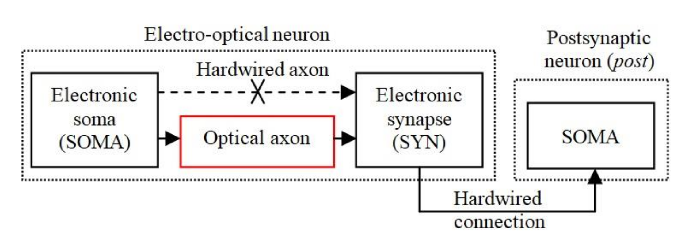
Figure 1 shows the basic structure of the EON implemented in analogue hardware, which includes an electronic soma (SOMA) for information processing, and at least one electronic synapse (SYN), which are used for weight storage and adaptability. The SOMA and SYN are connected optically by an OA for transmitting the trigger signals for activating the synapses. The electronic synapse, which transmits the weighted signals, is hardwired to the SOMA in order to reduce the effect of the optical induced noise sources. The SOMA and SYN represent the main elements of a bioinspired neuron model, which were implemented in analogue hardware reported in our previous work [47,48] and is adopted in this work.

Figure 1.
The general structure of the electro-optical neuron (EON) that includes a SOMA connected through the optical axon (OA) to a SYN.
A number of different forms of neuromorphic hardware with bioinspired plasticity rules have been reported in the literature [49], including the neuron model used in this work [47]. The SOMA models the integration of input stimuli detection of the activation threshold and refractory period as in [12], and the spike generation and the plasticity mechanisms are modeled by the SYN [47]. Note that in our previous work [12] the optical channel was implemented between the SYN output and the postsynaptic SOMA input, whereas in the current research the optical connection is between the SOMA output and the SYN input.
2.1. The Analogue Modules of the EON
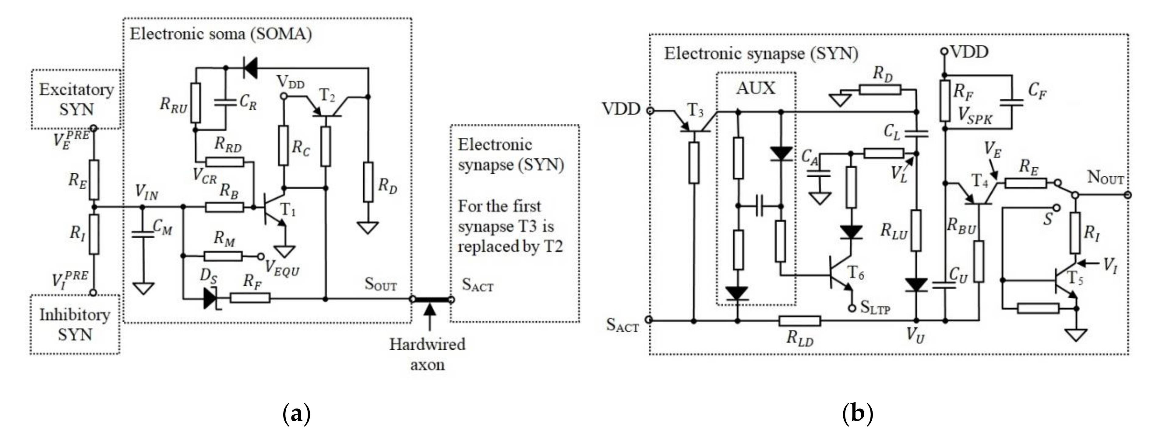
Figure 2 presents the schematic circuit diagram of the SOMA and SYN in which the axon is hardwired as in the original neuron design [47,48]. According to Figure 2a, during the neuron idle state, the voltage level across the capacitor is set to , which represents the equilibrium voltage of the artificial neuron.
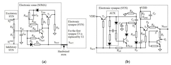
Figure 2.
The schematic of (a) the electronic SOMA and (b) the electronic synapse.
On activation of the SOMA, reaches the neuron activation threshold voltage , which for this neuron model is the transistor base-emitter voltage . During activation, the SOMA generates an active low pulse with a fixed width at for triggering, i.e., the SYNs which are connected to its output. The pulse width is determined by the capacity which is fully discharged during the neuron idle state. The discharge of determines the saturation time of following the time interval for all neuron activations. Note, the initial charge of does not change with , therefore the saturation time of and consequently the activation of OA are delayed by .
The input voltage across is given by:
where is the initial voltage across , , , and is the amplitude of the excitatory spike. The inhibitory stimulus (for which amplitude is typically ) is described by:
where , is the emitter resistor of , and is the discharge from . Note, if the SOMA is not activated, the equilibrium value of is restored via .
Considering that the analogue modules of the EON use transistors with , the model is then simplified for the case in which transistors are in the saturation or cut-off modes. During SOMA activation and when is in the saturation mode, is charged until is blocked. Thus, , , and determine the duration of the SOMA activation. At the same time, is discharged through to the forward voltage of the Schottky diode. This mimics the behaviour of the neural cell input potential, which is below the equilibrium voltage following activation. When the SOMA is activated, is pulled to , which varies with (i.e., the voltage stored in the learning capacitor ), as shown in Figure 2b.
Note that , which represents the synaptic weight, determines the saturation period of and consequently the generated spike duration and its energy. This excitatory output is given by:
where = for typical operation frequencies in the range of kHz, is the input potential of the post connected to , and is the emitter-base of . Note, with reference to Figure 2b the capacitor is discharged completly via during neuron activations thus maintaining the spike’s amplitude. However, using a set of and , the spike’s amplitude can be reduced due to the high activation frequency thus leading to reduced frequency of the postsynaptic neurons. From the biological point of view, this behavior of the electronic neuron can model the spike-frequency adaptation of the natural neurons, which shows a decrease in the spiking frequency of neurons following long activation periods [50,51].
The excitatory spike is converted into an inhibitory stimulus by an additional transistor connected as in Figure 2b. Considering that the response time of is negligible, the inhibitory output is given as:
Each SYN generates a spike at their output i.e., , which can be excitatory or inhibitory depending on the position of the switch . Note that, from the biological point of view, a neuron can include only excitatory or inhibitory synapses and not both. Thus, S is in the same position for all synapses in the AN. Taking into account that a neuron includes at least one synapse, included in the first SYN, see Figure 2b, is used instead of as shown in Figure 2a.
For this neuron model, increasing wS implies increasing/deceasing with decreasing/increasing wS (i.e., increasing the energy of the generated pulse). During neuron activation, decreases via , thus modeling the post-tetanic potentiation of the biological synapses. This presynaptic element of the synaptic plasticity represents weight adjustment when the neural cells are activated [52]. Furthermore, decreases when the postsynaptic activity occurs shortly after the activation of the SYN in concordance with the biological long-term potentiation [53]. This mechanism is implemented using , which temporarily discharges by . During the idle state that follows the neuron activation, the charge ΔQ is transferred back to if the post remains inactive. When the post is activated, the remaining stored in is discharged through the input , which is connected to of the postsynaptic SOMA. Note, the circuit AUX in Figure 2b is used to keep open until is discharged.
2.2. The Proposed OA
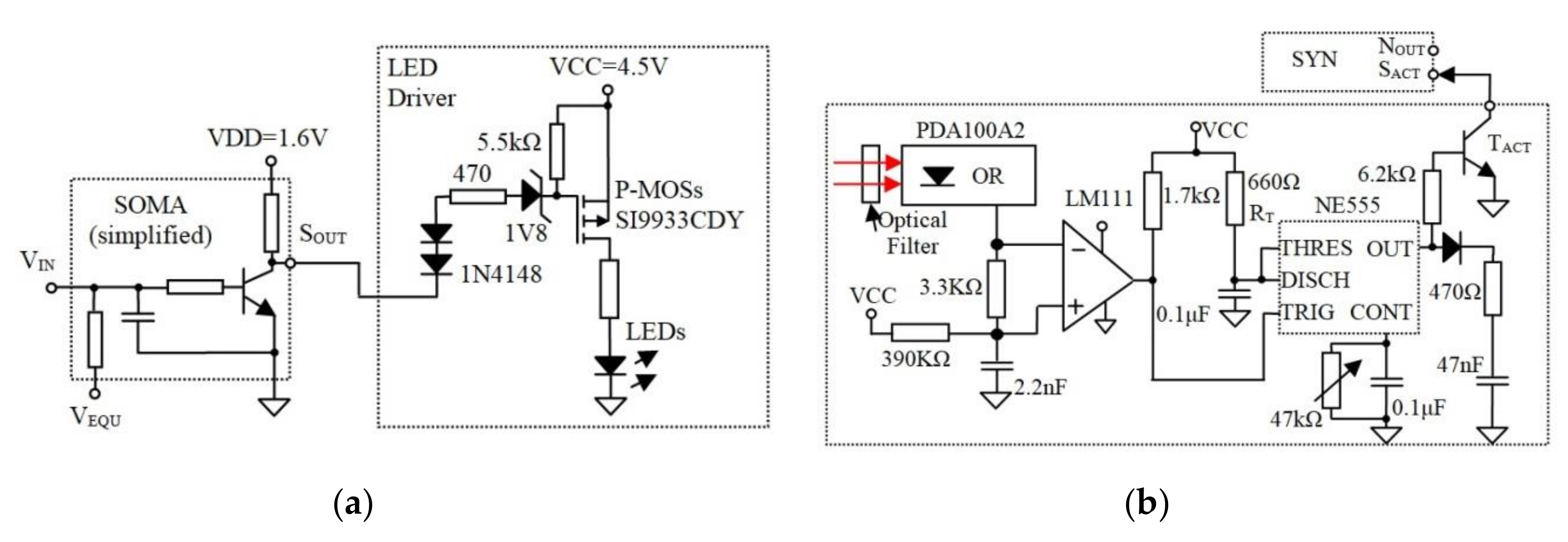
The concept introduced in this paper represents the OA, which is adapted to implement communication between distanced neural areas and to increase ONN operation tolerance to the beam intensity fluctuations. The OA structure shown in Figure 3 replaces the hardwired axon, which connects the SOMA to SYNs. At the transmitter (Tx), the OA includes a LED panel, which is intensity-modulated by the signals from the SOMA via the p-channel MOSFET transistors and the load resistor as in Figure 4a. At the receiver (Rx), an optical Rx (ORx) is used to regenerate the electrical signal, which is amplified and passed through a timer module for use by the SYN.
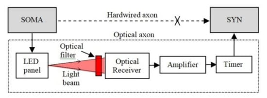
Figure 3.
The general structure of the OA including the LED panel at the Tx and the optical Rx, amplifier and timer on the Rx side.

Figure 4.
(a) The SOMA drives the LEDs using p-channel MOSFET transistors and (b) the Rx including the optical Rx and the additional circuitry that generate fixed-width pulses for SYN.
Note, the synaptic weight determines the generated pulse width Ts, therefore the duration of the SYN activation signal is critical. To reduce the changes (time jitter) in due to the channel induced perturbations, the electronic synapse is activated by a timer NE555; see Figure 4b.
3. Experimental Setup
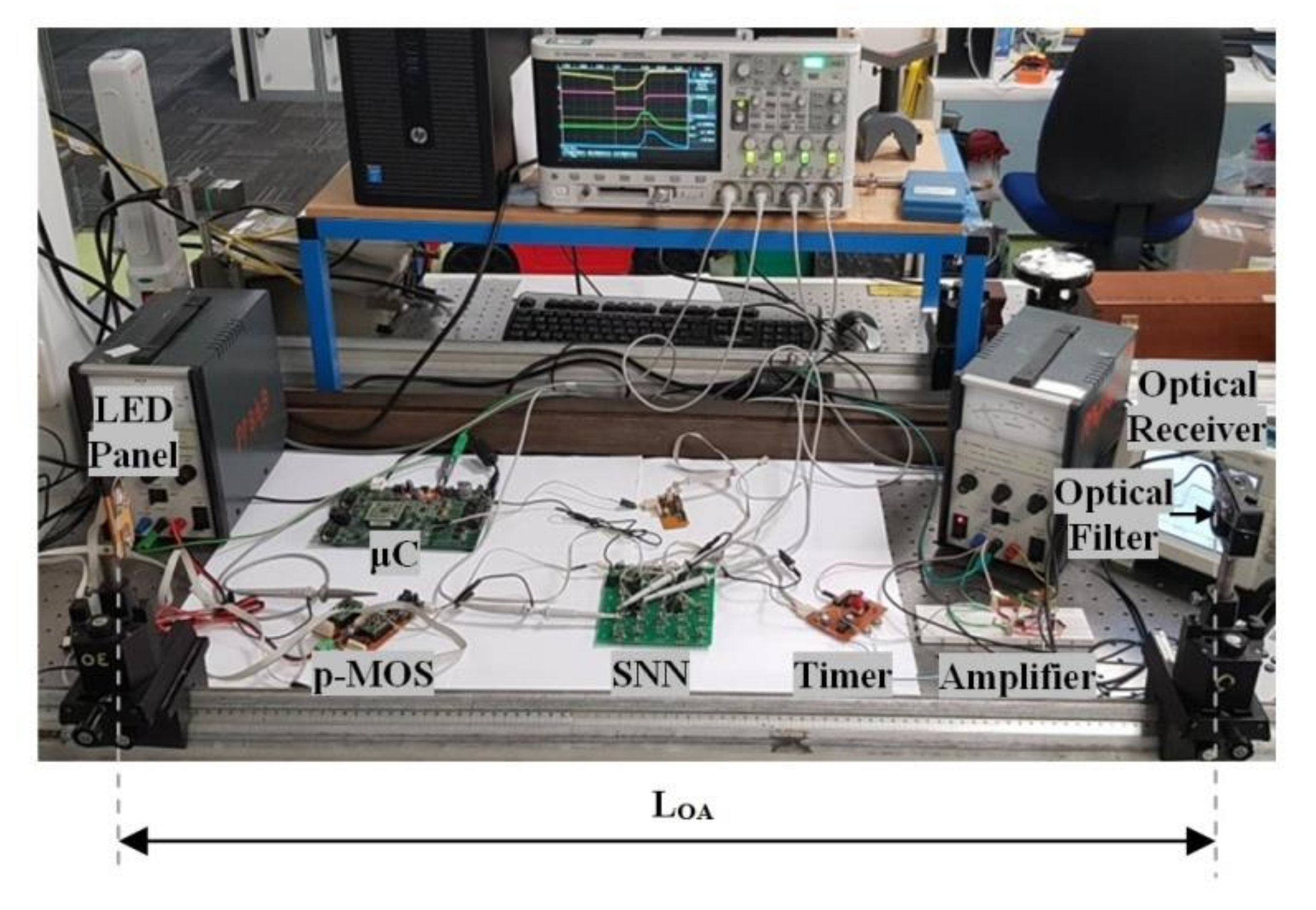
We developed an experimental testbed as shown in Figure 5 for evaluating the performance of the proposed system, in particular, the OA’s tolerance to the optical transmission range and the link misalignment. The system, with the key parameters given in Table 1, is composed of two OAs (i.e., OABLUE and OARED) for connecting two somas, SOMAB and SOMAR, to a synapse SYN, timer, SNN, optical filter, and ORx (Thorlabs PDA100A2).
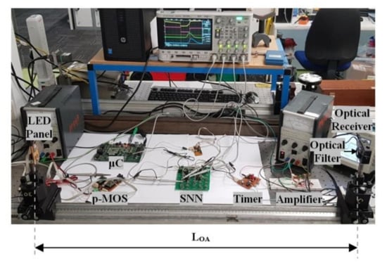
Figure 5.
The experimental setup.

Table 1.
System parameters.
Note, two SOMAs are used for activating the OA’s transmission wavelengths, OR’s sensitivity, and the drive current and illuminance for the LEDs. The SNN comprises SYNs and SOMAs, which are controlled by a microcontroller (μC). Experiments were performed in an indoor environment with an artificial room illuminance level of between 440 and 462 lux; see Table 1. At the receiving end, we used an optical filter to reduce the ambient light and therefore improve the signal-to-noise ratio. In [12,38], WDM systems with filters for parallel transmissions between optical neurons were reported, whereas a less costly version of WDM without filters was recently introduced in [54].
The output of the ORx is further amplified prior to being converted into a positive pulse with a fixed Tw using NE555; Figure 4b.
4. Results
The goal of the experiments was to evaluate the influence of the link length on the OA operation and how the system operates considering the link misalignment. The operation of the OA was analyzed independently for the red and blue LEDs using the same Rx. Because the spikes are transmitted using laser light sources in recent ONNs [13,36,37] due to speed, in this research we used LEDs due to the larger field of view which increases the tolerance to the link’s misalignment. The presented results are valid for OAs if activated simultaneously because the optical filters are used for channel isolation at the Rx. The two SOMAs are activated by a μC at sufficiently long periods when the SOMA’s input reaches the equilibrium voltage.
4.1. Delay Induced by the OA
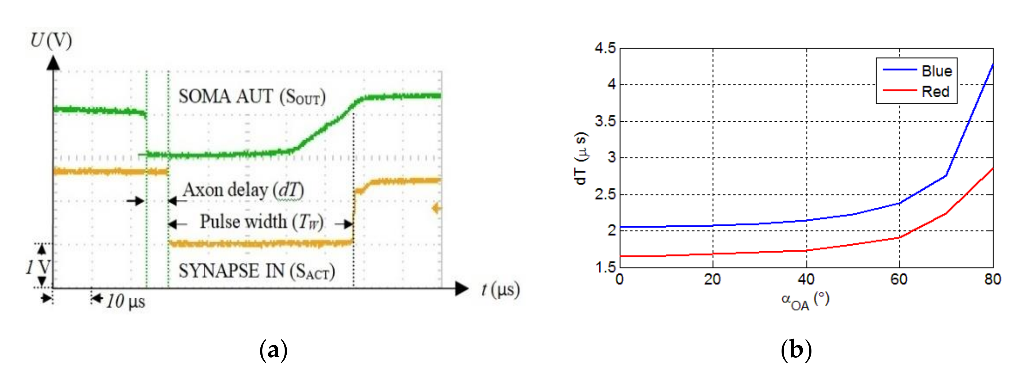
Because spike timing is the critical parameter in the SNN and SNs are temporal coincidence detectors, we measured the variation of the axon delay considering the link length and misalignment. Figure 6a shows the recorded signals when SOMAR activates the synapse SO through the OA, which generates a long pulse delayed by . Each value of was obtained for five consecutive measurements performed using the persistence function. Based on the data measured using the oscilloscope, the maximum jitter of the axon delay due to the optical channel is less than 0.4 μs for the maximum link span of 190 cm. The axon delay is determined by the beam intensity, which depends on the optical link length and the misalignment angle between the Tx and the Rx. For the evaluation tolerance of the OA on the link misalignment, the Tx was rotated at steps of 10° while the Rx was kept fixed.
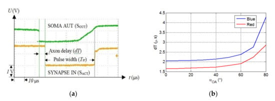
Figure 6.
(a) The measured time signals showing the soma output (upper signal) and the synapse input (lower signal), which is delayed by dT, and (b) the axon delay vs. for the red and blue LEDs and for
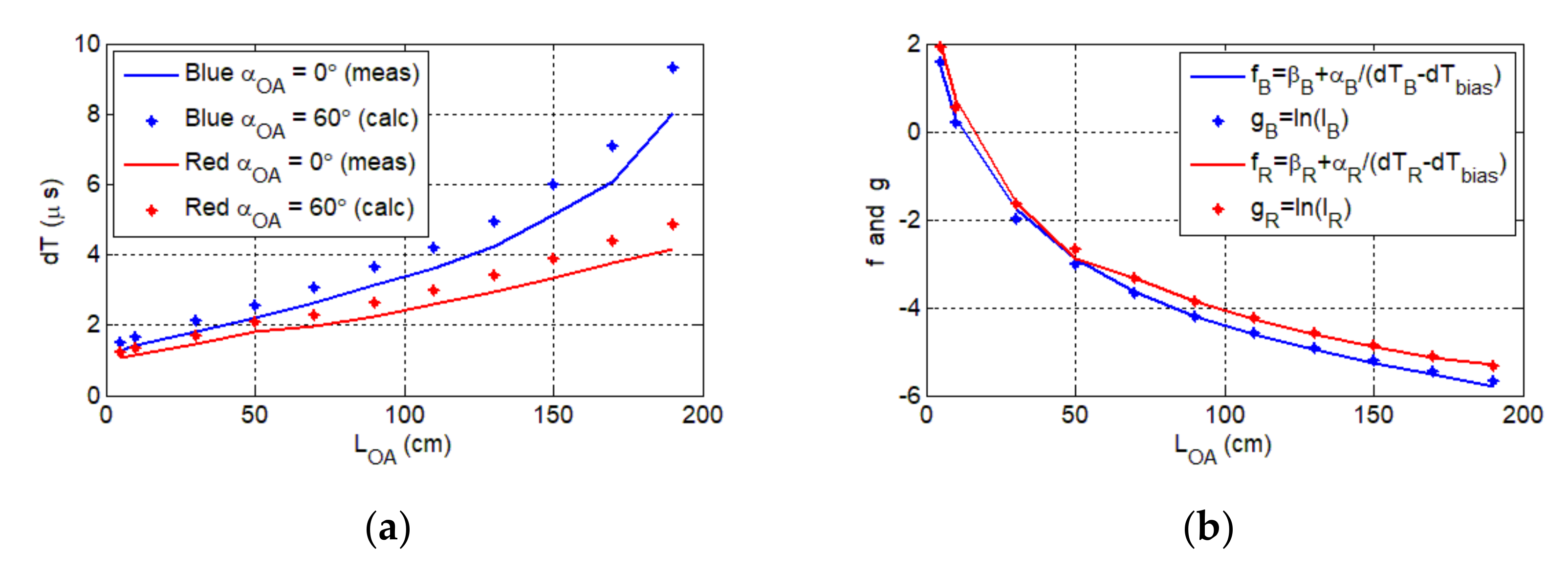
Figure 6b shows the variation of OA delay as a function of the rotation angle for an optical link length of 50 cm. Note, due to the symmetric beam profile, the Tx is rotated in only one direction. The maximum misalignment angle is , which is lower than half of the LED’s viewing angle of . This implies that at least three LEDs should be used to provide coverage. As shown, the OA delay increases exponentially with , with the blue LED displaying higher delays. Next, we investigated the delay as a function of the optical link span for both LEDs for of and , as shown in Figure 7a. For of and maximum , the measured are 8 and 4.2 μs for the blue and red LEDs, respectively.
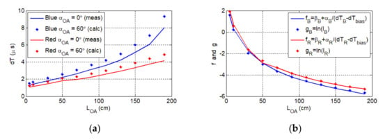
Figure 7.
(a) The delay vs. the optical link length (full line) for the aligned blue and red channels. The calculated axon delay for the maximum misalignment angle (dotted line). (b) The graphical representation of the relation between the photocurrent and the delay , respectively, for the red channel (red line and dots) and the blue channel (blue line and dots).
Note that the predicted axon delay for and variable was determined using the measured beam profiles for and , which is given as:
where is the delay for and variable . For the line of sight link the maximum measured delay , thus the axon may not be operational for > 170 cm and , where the predicted delay is above ; see Figure 7a. for the red channel is significantly lower than that of the blue channel. This is due to the higher irradiance level of the red LED and higher responsivity of the ORx at red wavelength; see Table 1.
4.2. Model for the Axon Delay
The axon delay was estimated by developing a model based on illuminance that fits . Thus, knowing the photocurrent in terms of the photopic efficacy and the Rx’s responsivity, ῃ can be determined as:
In addition, the measured has a component denoted by , which does not depend on . This delay is given by the response time of the electronics used between OR and SYN; see Figure 4b.
Because the Rx response depends on , we have the following functions as shown in Figure 7b:
where and the parameters and β are used for scaling on , which are given as:
The illuminance was determined for using , which was measured for ; see Table 1. Note the high similarity between and , for which the root mean square error (RMS) values are 0.98 and 0.95 for red and blue LEDs, respectively. Thus, the delay introduced by the OA is given by:
where and for the red channel, and and for the blue channel. The delay that yields the best RMS for both wavelengths is This value is practically plausible considering the parameters of OR, LM111, NE555, and BC848 that are used to activate the synapse.
5. Axon Delay Influence on Neuron Activity
In this section, we determined the tolerance of the SNN to the maximum axon delay. Typically, wireless communications are suitable for neural areas that are connected via OAs. To determine whether the delays affect SNN behavior, we implemented a network that includes two electronic synapses (SYN1 and SYN2), which stimulate a SOMA; see Figure 8a.

Figure 8.
(a) Structure of the spiking neural network (SNN), which includes two synapses and a soma for testing the influence of the axon delay on the activations of the neurons; (b) the microcontroller was programmed to generate delays between pulses that activate two synapses through inputs and .
To simplify the test process and to ensure repeatability of the results, the synapses were activated by pulse trains with different delays generated using a microcontroller (see Figure 8b), which simulates the axon’s output. The activity of the postsynaptic neuron was evaluated by monitoring the SOMA activation period for in the range of with a resolution of 0.7 μs. The measurements show that, for the maximum , increases by less than . The natural neurons operate typically at a few tens of Hz [55] with the maximum frequency observed in the human brain [56]. This gives the minimum time interval between neuron activations of . Note, is less than 0.5% of the inter-spike period , implying that the influence of the axon delay on the biologically plausible frequency of spiking neurons is negligible.
6. Discussions
The results show that light intensity fluctuations do not influence the duration of the SOMA activation, thus lessening the effects on transmission of synaptic weights. During the experiments, the light intensity varied significantly (i.e., by two orders of magnitude), which implies that implementation of LIM is not feasible because it directly converts the synaptic weights into light intensity [13,36]. Note that an ONN based on spiking neurons typically converts the synaptic weights into the spikes’ amplitude and duration [12], therefore conversion of spikes into optical pulses will be susceptible to light intensity fluctuations. This is because changes in the amplitude of the optical pulse means modified synaptic weights.
Conversely, the OA induces a delay, which depends on the optical channel characteristics (i.e., length, alignment, and components) that affect the SNN operation by changing the frequency of the spiking neurons, thus affecting the polychronization of the SNN [57]. Recent research shows that the precision of electronic neurons can be as low as 50 ns in the detection of temporal stimuli [58]. This order of magnitude for OA delay can be reached using faster electronics. As an example, can be reduced below 30 ns for ( using the ultrafast Tx with the response time [59], in addition to a fast Rx implemented with FPD310 (, comparator LMH7220 (, and fixed-width pulse generator based on ultra-fast logic gates (); see the OA structure in Figure 1. However, because increasing the communication distance between neural areas results in non-compensable delays, one possible option to reduce the OA influence on the SNN would be to decrease the neuron’s frequency. Low-speed analogue hardware platforms will increase the tolerance of the SNN to the increased transmission spans. The possible applications that can benefit from the proposed optical axons are bio-inspired systems, including neuromorphic sensors [4,40], with a built-in preprocessing neural layer. The tolerance of the OA to the variation of the channel length and link misalignment makes the OA suitable for exploration applications in which neuromorphic sensors are mobile. In addition, the OA could be used in the implementation of brain–computer interfaces [60] or in the recently tested brain-to-brain communications [61,62].
In practical applications, the maximum number of inputs and outputs of the system will determine the number of parallel free space channels (i.e., free space with WDM) that could be used. For the single-color LED-based Txs, is determined by the number of available wavelengths within the range of 250–1650 nm. Note, higher and (i.e., up to 70) can be employed by using a combination of broad-band LEDs and narrow-band optical bandpass filters (OBPF), and a high-bandwidth PD. However, because of the limited dynamic range of the optical Tx and Rx and their dependency on λ, in addition to system complexity, about 35 channels should be used.
7. Conclusions
A common method to encode synaptic weights in optical neural networks is light intensity modulation. In free space-based ONNs, the weights are affected by beam fading due to variation in the distance between neural areas. This paper presented the theoretical and practical implementation of a new and efficient method to significantly reduce the effects of beam fading in free space optical-based neural networks. The proposed method is based on optical axons, which eliminate the requirement for synaptic weight transmission over the free optical channels. OAs could be used to implement the optical connections in multi-modular bioinspired systems, which include mobile neuromorphic sensors. For testing this novel concept, we determined the delay induced by two OAs with different parameters. Results showed that the delay is significantly influenced by the axon parameters of light intensity and the responsivity of the optical Rx. Thus, based on experimental data we developed a model to estimate the delay as a function of illuminance. The maximum axon length and the delay achieved were 190 cm and respectively, for the line of sight transmission. It was shown that the influence of the axon delay on the biologically plausible frequency of spiking neurons is insignificant for the considered SNN that operates in the kHz range. For faster SNNs, lower values of OA delay can be achieved using high-speed electronic circuitry. However, OA integration in ultrafast photonic NNs has limitations determined by the speed of light.
In future work we will (i) carry out testing and measurement of the associative learning mechanisms with optical axons used in ONNs, and increase the number of channels; and (ii) focus on the evaluation of an anthropomorphic robotic arm with the neuromorphic rotation and force sensors connected optically to the main SNN.
Author Contributions
Conceptualization, M.H.; methodology, M.H., Z.G., and O.I.Y.; validation, Z.G., S.R. and O.I.Y.; formal analysis, M.H. and Z.G.; investigation, M.H., O.I.Y. and A.B.; data curation, O.I.Y.; writing—original draft preparation, M.H.; writing—review and editing, Z.G., S.R., and O.I.Y.; supervision, Z.G. and S.R.; resources, A.B.; All authors have read and agreed to the published version of the manuscript.
Funding
This work was supported by the EU COST Action CA19111: NEWFOCUS, and by the National Research Grant of the TUIASI, project number GnaC2018 66/01.03.2019.
Conflicts of Interest
The authors declare no conflict of interest.
Nomenclature
| Short Form | Description |
| AN | Artificial neuron |
| ANN | Artificial neural networks |
| BPOF | Band pass optical filters |
| EON | Electro-optical neurons |
| FWHM | Full width half maximum |
| LED | Light emitting diode |
| LIM | Light intensity modulation |
| OA | Optical axon |
| ONN | Optical neural networks |
| OR | Optical receiver |
| PD | Photodiode |
| PNN | Photonic neural networks |
| Rx | Receiver |
| SNN | Spiking neural networks |
| SOMA | Input module of the electronic neuron |
| SYN | Electronic synapse |
| Tx | Transmitter |
| ws | Weights |
| WDM | Wavelength division multiplexing |
| μC | Microcontroller |
References
- Maass, W. Networks of spiking neurons: The third generation of neural network models. Neural Netw. 1997, 10, 1659–1671. [Google Scholar]
- Kasabov, N. Deep learning of multisensory streaming data for predictive modelling with applications in finance, ecology, transport and environment. In Time-Space, Spiking Neural Networks and Brain-Inspired Artificial Intelligence; Springer: Berlin/Heidelberg, Germany, 2019; pp. 619–658. [Google Scholar]
- Pfeiffer, M.; Pfeil, T. Deep learning with spiking neurons: Opportunities and challenges. Front. Neurosci. 2018, 12, 774. [Google Scholar] [CrossRef]
- Indiveri, G. Neuromorphic VLSI models of selective attention: From single chip vision sensors to multi-chip systems. Sensors 2008, 8, 5352–5375. [Google Scholar] [PubMed]
- Vogelstein, R.J.; Mallik, U.; Culurciello, E.; Cauwenberghs, G.; Etienne-Cummings, R. Saliency-driven image acuity modulation on a reconfigurable array of spiking silicon neurons. Adv. Neural Inf. Process. Syst. 2005, 1457–1464. [Google Scholar]
- Wunderlich, T.; Kungl, A.; Müller, E.; Hartel, A.; Stradmann, Y.; Aamir, S.A.; Grübl, A.; Heimbrecht, A.; Schreiber, K.; Stöckel, D.; et al. Demonstrating advantages of neuromorphic computation: A pilot study. Front. Neurosci. 2019. [Google Scholar] [CrossRef]
- Mostafa, H. Supervised learning based on temporal coding in spiking neural networks. IEEE Trans. Neural Netw. Learn. Syst. 2018, 29, 3227–3235. [Google Scholar] [PubMed]
- Liu, S.C.; Delbruck, T. Neuromorphic sensory systems. Curr. Opin. Neurobiol. 2010, 20, 288–295. [Google Scholar] [PubMed]
- Boahen, K. A neuromorph’s prospectus. Comput. Sci. Eng. 2017, 19, 14–28. [Google Scholar]
- Esser, S.K.; Merolla, P.A.; Arthur, J.V.; Cassidy, A.S.; Appuswamy, R.; Andreopoulos, A.; di Nolfo, C.; Datta, P.; Amir, A.; Taba, B.; et al. From the cover: Convolutional networks for fast, energy-efficient neuromorphic computing. Proc. Natl. Acad. Sci. USA 2016, 113, 11441. [Google Scholar] [PubMed]
- Pfister, J.-P.; Gerstner, W. Triplets of spikes in a model of spike timing-dependent plasticity. J. Neurosci. 2006, 26, 9673–9682. [Google Scholar]
- Hulea, M.; Ghassemlooy, Z.; Rajbhandari, S. Spiking neural network with visible light communication. In Proceedings of the 11th International Symposium on Communication Systems, Networks & Digital Signal Processing (CSNDSP), Budapest, Hungary, 18–20 July 2018. [Google Scholar] [CrossRef]
- Tait, A.; de Lima, T.F.; Zhou, E.; Wu, A.; Nahmias, M.; Shastri, B.; Prucnal, P. Neuromorphic photonic networks using silicon photonic weight banks. Sci. Rep. Nat. 2017, 7, 7430. [Google Scholar] [CrossRef]
- Nahmias, M.; Shastri, B.; Tait, A.; de Lima, T.F.; Prucnal, P. Principles of neuromorphic photonics. Opt. Photonics News 2018, 29, 34–41. [Google Scholar] [CrossRef]
- Peng, H.-T.; Nahmias, M.; de Lima, T.F.; Tait, A.; Shastri, B.J.; Prucnal, P. Neuromorphic photonic integrated circuits. IEEE J. Sel. Top. Quantum Electron. 2018, 24. [Google Scholar] [CrossRef]
- Shastri, B.; Tait, A.; Nahmias, M.; Prucnal, P. Photonic spike processing: Ultrafast laser neurons and an integrated photonic network. IEEE Photonics Soc. Newsl. 2014, 28, 4–11. [Google Scholar]
- Uysal, M.; Capsoni, C.; Ghassemlooy, Z.; Boucouvalas, A.C.; Udvary, E.G. Optical Wireless Communications—An Emerging Technology; Springer: Berlin, Germany, 2016; ISBN 978-3-319-30200-3. [Google Scholar]
- Farhat, N.; Psaltis, D.; Prata, A.; Paek, E. Optical implementation of the Hopfield model. Appl. Opt. 1985, 24, 1469–1475. [Google Scholar] [CrossRef] [PubMed]
- De Groot, P.; Noll, R. Adaptive neural network in a hybrid optical/electronic architecture using lateral inhibition. Appl. Opt. 1989, 28, 3852–3859. [Google Scholar] [CrossRef]
- Jutamulia, S.; Yu, F.T.S. Overview of hybrid optical neural networks. Opt. Laser Technol. 1996, 28, 59–72. [Google Scholar] [CrossRef]
- Mourgias-Alexandris, G.; Tsakyridis, A.; Passalis, N.; Tefas, A.; Vyrsokinos, K.; Pleros, N. An all-optical neuron with sigmoid activation function. Opt. Express 2019, 27, 9620–9630. [Google Scholar] [CrossRef] [PubMed]
- Fang, M.; Manipatruni, S.; Wierzynski, C.; Khosrowshahi, A.; Deweese, M. Design of optical neural networks with component imprecisions. Opt. Express 2019, 27, 14009–14029. [Google Scholar] [CrossRef]
- Hughes, T. Training of photonic neural networks through in situ backpropagation. Optica 2018, 5, 864–871. [Google Scholar] [CrossRef]
- Chakraborty, I.; Saha, G.; Sengupta, A.; Roy, K. Toward fast neural computing using all-photonic phase change spiking neurons. Sci. Rep. Nat. 2018, 8, 12980. [Google Scholar] [CrossRef] [PubMed]
- Tait, A.; Ferreira de Lima, T.; Nahmias, M.; Miller, H.; Peng, H.-T.; Shastri, B.; Prucnal, P. A silicon photonic modulator neuron. Phys. Rev. Appl. 2019, 11, 064043. [Google Scholar] [CrossRef]
- Fiers, M.; Morthier, G.; Verstraeten, D.; Schrauwen, B.; Dambre, J.; Bienstman, P. Experimental demonstration of reservoir computing on a silicon photonics chip. Nat. Commun. 2014, 5, 3541. [Google Scholar]
- Tait, A.; Zhou, E.; Wu, A.; Nahmias, M.; de Lima, T.F.; Shastri, B.; Prucnal, P. Demonstration of a silicon photonic neural network. In Proceedings of the 2016 IEEE Photonics Society Summer Topical Meeting Series (SUM), Newport Beach, CA, USA, 11–13 July 2016; pp. 72–73. [Google Scholar]
- Feldmann, J.; Youngblood, N.; Wright, C.D.; Bhaskaran, H.; Pernice, W.H.P. All-optical spiking neurosynaptic networks with self-learning capabilities. Nature 2019, 569, 208–214. [Google Scholar] [CrossRef] [PubMed]
- Zhuge, X.; Wang, J.; Zhuge, F. Photonic synapses for ultrahigh-speed neuromorphic computing. Rapid Res. Lett. 2019, 13, 190082. [Google Scholar] [CrossRef]
- George, J.; Mehrabian, A.; Amin, R.; Meng, J.; de Lima, T.F.; Tait, A.; Shastri, B.; El-Ghazawi, T.; Prucnal, P.; Sorger, V. Neuromorphic photonics with electro-absorption modulators. Opt. Express 2019, 27, 5181–5191. [Google Scholar] [CrossRef]
- Hu, D.-C.; Yang, R.; Jiang, L.; Guo, X. Memristive synapses with photoelectric plasticity realized in zno1–x/aloy heterojunction. ACS Appl. Mater. Interfaces 2018, 10, 6463. [Google Scholar] [CrossRef] [PubMed]
- Qin, S.; Liu, Y.; Wang, X.; Xu, Y.; Shi, Y.; Zhang, R.; Wang, F. Photonic synaptic device capable of optical memory and logic operations. In Proceedings of the 2017 Conference on Lasers and Electro-Optics (CLEO), San Jose, CA, USA, 14–19 May 2017; pp. 1–2. [Google Scholar]
- Lee, M.; Lee, W.; Choi, S.; Jo, J.W.; Kim, J.; Park, S.K.; Kim, Y.H. Brain-inspired photonic neuromorphic devices using photodynamic amorphous oxide semiconductors and their persistent photoconductivity. Adv. Mater. 2017, 29, 1700951. [Google Scholar]
- Agnus, G.; Zhao, W.; Derycke, V.; Filoramo, A.; Lhuillier, Y.; Lenfant, S.; Vuillaume, D.; Gamrat, C.; Bourgoin, J.-P. Two-terminal carbon nanotube programmable devices for adaptive architectures. Adv. Mater. 2010, 22, 702–706. [Google Scholar] [CrossRef]
- Lee, Y.; Oh, Y.; Xu, W.; Kim, O.; Kim, T.R.; Kang, J.; Kim, Y.; Son, D.; Tok, J.; Park, M.J.; et al. Stretchable organic optoelectronic sensorimotor synapse. Sci. Adv. 2018, 4, eaat7387. [Google Scholar] [CrossRef]
- Tait, A.; Wu, A.; de Lima, T.F.; Zhou, E.; Shastri, B.; Nahmias, M.; Prucnal, P. Microring weight banks. IEEE J. Sel. Topics Quantum Electron. 2016, 22, 5900214. [Google Scholar] [CrossRef]
- Tait, A.; Nahmias, M.; Shastri, B.; Prucnal, P. Broadcast and weight: An integrated network for scalable photonic spike processing. J. Lightw. Technol. 2014, 32, 4029–4041. [Google Scholar] [CrossRef]
- Nawrocka, M.; Liu, T.; Wang, X.; Panepucci, R. Tunable silicon microring resonator with wide free spectral range. Appl. Phys. Lett. 2006, 89, 071110. [Google Scholar] [CrossRef]
- Moayedi Pour Fard, M.; Williamson, I.; Edwards, M.; Liu, K.; Pai, S.; Bartlett, B.; Minkov, M.; Hughes, T.; Fan, S.; Nguyen, T. Experimental realization of arbitrary activation functions for optical neural networks. Opt. Express 2020, 28, 12138. [Google Scholar] [CrossRef] [PubMed]
- Vanarse, A.; Osseiran, A.; Rassau, A. A review of current neuromorphic approaches for vision, auditory, and olfactory sensors. Front. Neurosci. 2016, 10, 115. [Google Scholar] [CrossRef]
- Vanarse, A.; Osseiran, A.; Rassau, A. An Investigation into Spike-Based Neuromorphic Approaches for Artificial Olfactory Systems. Sensors 2017, 17, 2591. [Google Scholar] [CrossRef]
- Vanarse, A.; Osseiran, A.; Rassau, A. Real-time classification of multivariate olfaction data using spiking neural networks. Sensors 2019, 19, 1841. [Google Scholar] [CrossRef] [PubMed]
- Vanarse, A.; Osseiran, A.; Rassau, A.; van der Made, P. A hardware-deployable neuromorphic solution for encoding and classification of electronic nose data. Sensors 2019, 19, 4831. [Google Scholar] [CrossRef] [PubMed]
- Zhang, X.; Zhuo, Y.; Luo, Q.; Wu, Z.; Midya, R.; Wang, Z.; Song, W.; Wang, R.; Upadhyay, N.; Fang, Y.; et al. An artificial spiking afferent nerve based on Mott memristors for neurorobotics. Nat. Commun. 2020, 11, 51. [Google Scholar] [CrossRef]
- Hulea, M.; Uleru, G.; Burlacu, A.; Caruntu, C. Bioinspired SNN for robotic joint control. In Proceedings of the 2020 IEEE International Conference on Automation, Quality and Testing, Robotics (AQTR), Cluj-Napoca, Romania, 21–23 May 2020; pp. 1–5. [Google Scholar]
- Hulea, M.; Burlacu, A.; Caruntu, C.F. Intelligent motion planning and control for robotic joints using bio-inspired spiking neural networks. Int. J. Hum. Robot. 2019, 16, 1950012. [Google Scholar] [CrossRef]
- Hulea, M. Electronic Circuit for Modeling an Artificial Neuron. Romanian Patent RO-126249; priority date: 29.04.2011, granted, 29 November 2018. [Google Scholar]
- Hulea, M. The mathematical model of a biologically inspired electronic neuron for ease the design of spiking neural networks topology. In Proceedings of the 15th International Conference on System Theory, Control and Computing (ICSTCC), Sinaia, Romania, 14–16 October 2011; pp. 1–6. [Google Scholar]
- Schuman, C.D.; Potok, E.T.; Patton, R.M.; Birdwell, J.D.; Dean, E.M.; Rose, S.G.; Plank, S.J. A survey of neuromorphic computing and neural networks in hardware. arXiv 2017, arXiv:1705.06963. [Google Scholar]
- Fairhall, A.L.; Lewen, G.D.; Bialek, W.; van Steveninck, R.R.D.R. Efficiency and ambiguity in an adaptive neural code. Nature 2001, 412, 787–792. [Google Scholar] [CrossRef] [PubMed]
- Pozzorini, C.; Naud, R.; Mensi, S.; Gerstner, W. Temporal whitening by power-law adaptation in neocortical neurons. Nat. Neurosci. 2013, 16, 942–948. [Google Scholar] [CrossRef] [PubMed]
- Brager, D.; Cai, X.; Thompson, S. Activity-dependent activation of presynaptic protein kinase C mediates post-tetanic potentiation. Nat. Neurosci. 2003, 6, 551–552. [Google Scholar] [CrossRef] [PubMed]
- Whitlock, J.R.; Heynen, A.J.; Shuler, M.G.; Bear, M.F. Learning induces long-term potentiation in the hippocampus. Science 2016, 313, 1093–2006. [Google Scholar] [CrossRef] [PubMed]
- Burton, A.; Haigh, P.A.; Chvojka, P.; Ghassemlooy, Z.; Zvánovec, S. Filter-less WDM for visible light communications using colored pulse amplitude modulation. Opt. Lett. 2019, 44, 4849–4852. [Google Scholar] [CrossRef] [PubMed]
- Zambrano, D.; Nusselder, R.; Scholte, H.S.; Bohté, S.M. Sparse computation in adaptive spiking neural networks. Front. Neurosci. 2019, 12, 987–998. [Google Scholar] [CrossRef] [PubMed]
- Wang, B.; Ke, W.; Guang, J.; Chen, G.; Yin, L.; Deng, S.; He, Q.; Liu, Y.; He, T.; Zheng, R.; et al. Firing frequency maxima of fast-spiking neurons in human, monkey and mouse neocortex. Front. Cell Neurosci. 2016, 10, 239. [Google Scholar] [CrossRef]
- Izhikevich, E.M. Polychronization: Computation with spikes. Neural Comput. 2006, 18, 245–282. [Google Scholar] [CrossRef]
- Pfeil, T.; Scherzer, A.-C.; Schemmel, J.; Meier, K. Neuromorphic learning towards nano second precision. In Proceedings of the 2013 International Joint Conference on Neural Networks (IJCNN), Dallas, TX, USA, 4–9 August 2013; pp. 1–5. [Google Scholar]
- Gong, C.; Lee, Y.-C.; Lai, J.L.; Yu, C.H.; Huang, L.R.; Yang, C.Y. The high-efficiency led driver for visible light communication applications. Sci. Rep. 2016, 6, 30991. [Google Scholar] [CrossRef]
- Alonso, L.F.N.; Gil, J.G. Brain Computer Interfaces, A Review. Sensors 2012, 12, 1211–1279. [Google Scholar]
- Jiang, L.; Stocco, A.; Losey, D.M.; Abernethy, A.J.; Prat, S.C.; Rao, R.P.N. BrainNet: A Multi-Person Brain-to-Brain Interface for Direct Collaboration Between Brains. Sci. Rep. 2019, 9, 6115. [Google Scholar] [PubMed]
- Grau, C.; Ginhoux, R.; Riera, A.; Lam Nguyen, T.; Chauvat, H.; Berg, M.; Amengual, J.; Pascual-Leone, A.; Ruffini, G. Conscious brain-to-brain communication in humans using non-invasive technologies. PLoS ONE 2014, 9, e105225. [Google Scholar]
Publisher’s Note: MDPI stays neutral with regard to jurisdictional claims in published maps and institutional affiliations. |
© 2020 by the authors. Licensee MDPI, Basel, Switzerland. This article is an open access article distributed under the terms and conditions of the Creative Commons Attribution (CC BY) license (http://creativecommons.org/licenses/by/4.0/).

