Implementation of Analog Perceptron as an Essential Element of Configurable Neural Networks


Abstract
1. Introduction
2. Preliminary
2.1. Motivation for Analog-Based MLP Implementation
2.2. Configurable Neural Networks Based on Analog Perceptron
3. A Measurement-Verified Perceptron Chip
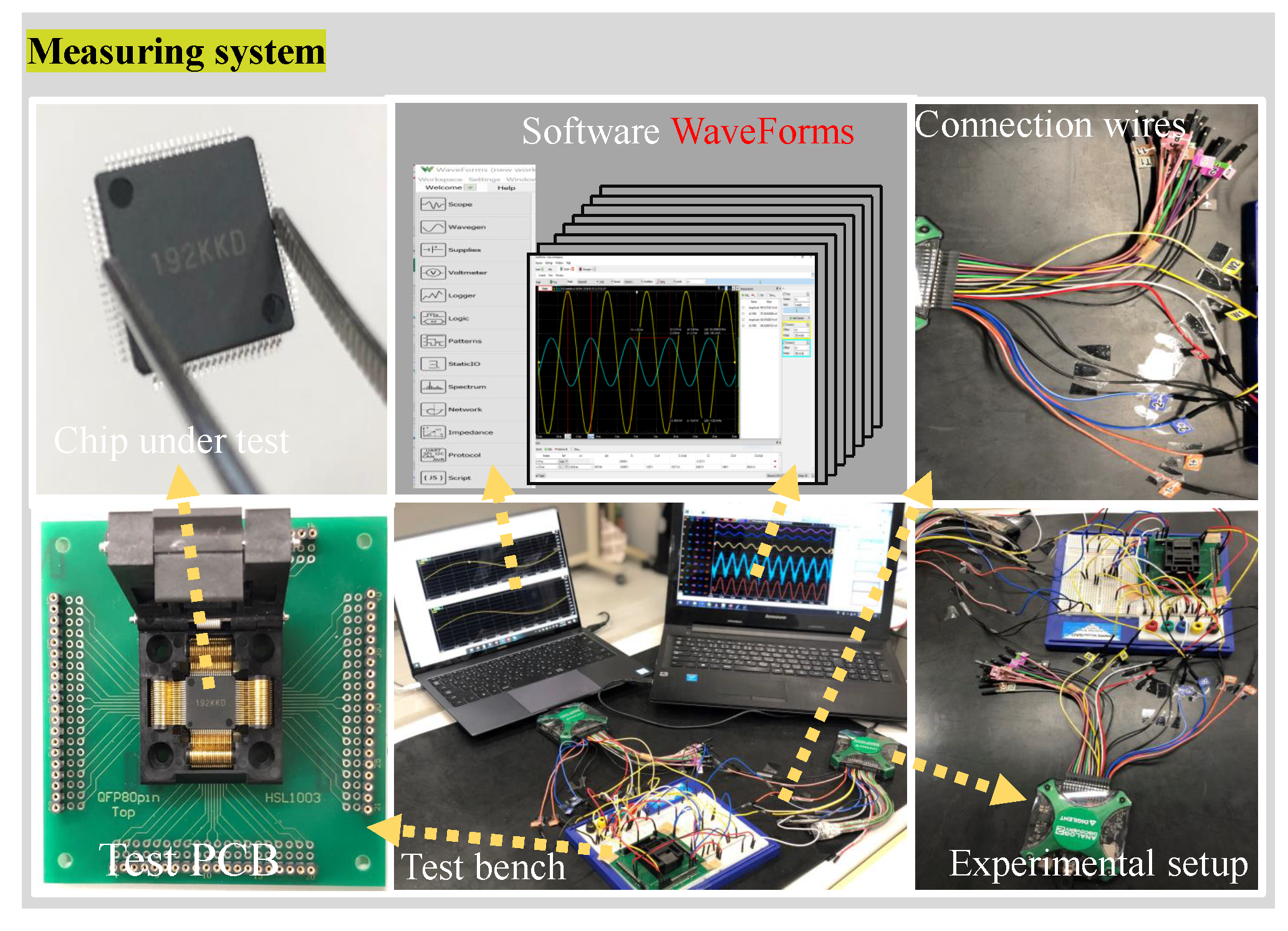
3.1. A Measuring System for Perceptron Chip
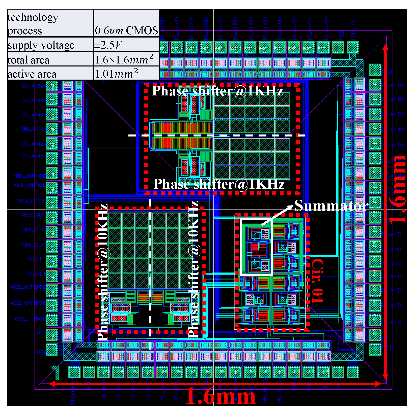
3.2. Schematic and Layout for the Circuits under Test
3.3. The Measurement Result and Analysis
4. An MLP Circuit for Configurable Neural Network
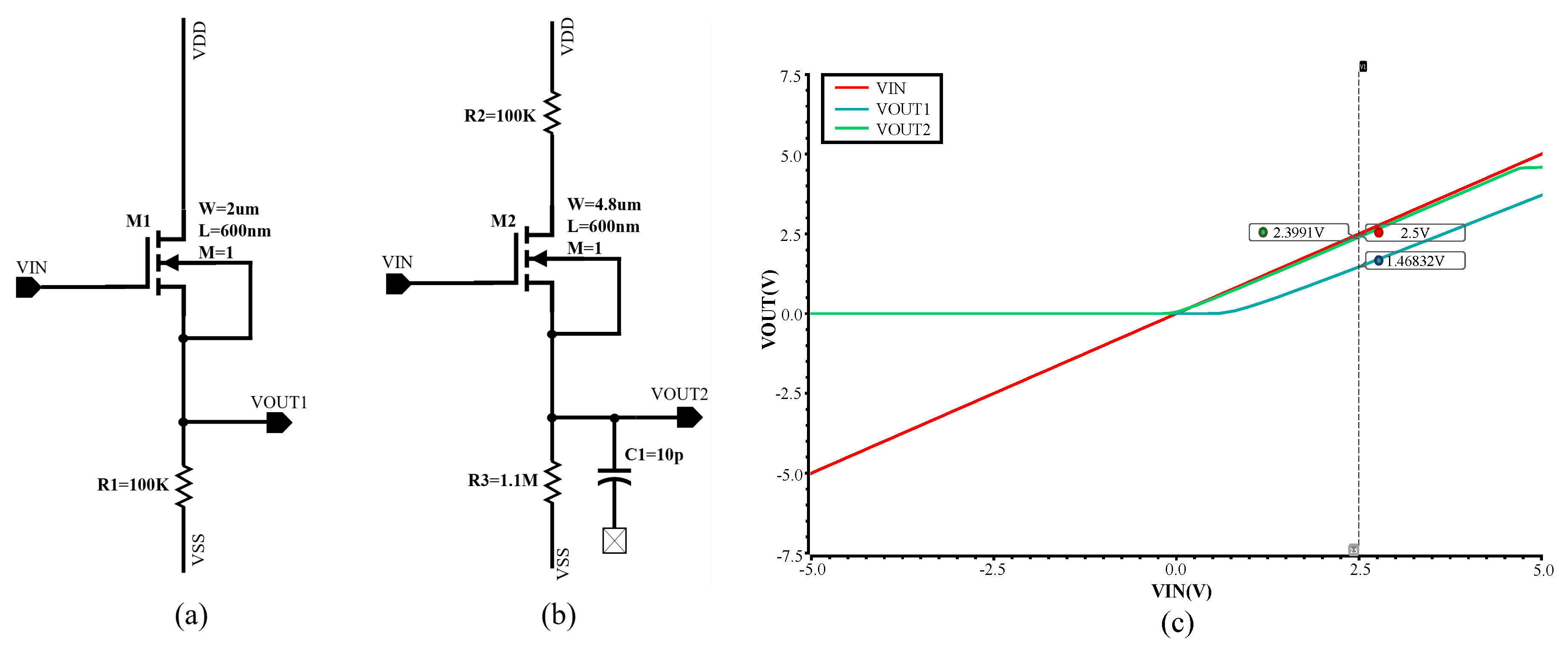
4.1. An Improved Source Follower
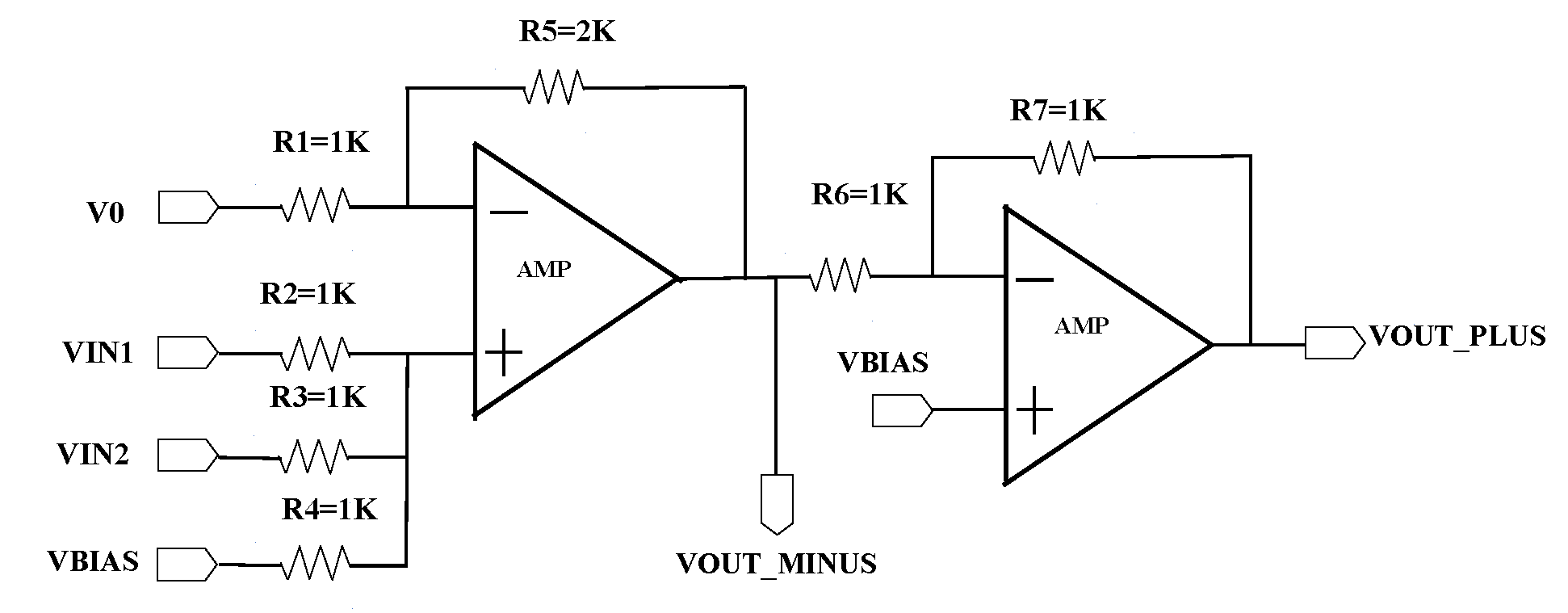
4.2. Summator for Improving Reliability
4.3. Impedance Issue of Cascading Neurons
5. Experimental Case for MLP Circuit
5.1. Simulation Explanation
5.2. Summary and Discussion of MLP Circuit
6. Conclusions
Author Contributions
Funding
Conflicts of Interest
References
- Alom, M.Z.; Taha, T.M.; Yakopcic, C.; Westberg, S.; Sidike, P.; Nasrin, M.S.; Hasan, M.; Van Essen, B.C.; Awwal, A.A.; Asari, V.K. A State-of-the-Art Survey on Deep Learning Theory and Architectures. Electronics 2019, 8, 292. [Google Scholar] [CrossRef]
- Du, Y.; Du, L.; Gu, X.; Du, J.; Wang, X.S.; Hu, B.; Jiang, M.; Chen, X.; Iyer, S.S.; Chang, M.C.F. An Analog Neural Network Computing Engine Using CMOS-Compatible Charge-Trap-Transistor (CTT). IEEE Trans. Comput. Aided Des. Integr. Circuits Syst. 2019, 38, 1811–1819. [Google Scholar] [CrossRef]
- Yen, C.; Weng, W.; Lin, Y. FPGA Realization of a Neural-Network-Based Nonlinear Channel Equalizer. IEEE Trans. Ind. Electron. 2004, 51, 472–479. [Google Scholar] [CrossRef]
- Maliuk, D.; Makris, Y. A dual-mode weight storage analog neural network platform for on-chip applications. In Proceedings of the IEEE International Symposium on Circuits and Systems, Seoul, Korea, 20–23 May 2012; pp. 2889–2892. [Google Scholar] [CrossRef]
- Horita, T.; Takanami, I. An FPGA-based multiple-weight-and-neuron-fault tolerant digital multilayer perceptron. Neurocomputing 2013, 99, 570–574. [Google Scholar] [CrossRef]
- Aravindan, M.; Kingsley, S. Recognition of modulation using Multilayer perceptron in digital communication. In Proceedings of the 2011 IEEE Recent Advances in Intelligent Computational Systems, Trivandrum, Kerala, India, 22–24 September 2011; pp. 264–268. [Google Scholar] [CrossRef]
- Kawaguchi, M.; Ishii, N.; Umeno, M. Analog Learning Neural Circuit with Switched Capacitor and the Design of Deep Learning Model. In Proceedings of the International Conference on Computational Science/Intelligence & Applied Informatics, Okayama, Japan, 12–16 July 2015; Springer: Okayama, Japan, 2015; pp. 93–107. [Google Scholar] [CrossRef]
- Neckar, A.; Stewart, T.C.; Benjamin, B.V.; Boahen, K. Optimizing an Analog Neuron Circuit Design for Nonlinear Function Approximation. In Proceedings of the 2018 IEEE International Symposium on Circuits and Systems (ISCAS), Florence, Italy, 27–30 May 2018; pp. 1–5. [Google Scholar] [CrossRef]
- Lont, J.; Guggenbuhl, W. Analog CMOS implementation of a multilayer perceptron with nonlinear synapses. IEEE Trans. Neural Netw. 1992, 3, 457–465. [Google Scholar] [CrossRef] [PubMed]
- Zatorre, G.; Sanz, M.T.; Medrano, N.; Martinez, P.A.; Celma, S. An Analogue CMOS Neural Circuit for Improved Sensing. In Proceedings of the 2006 Ph.D. Research in Microelectronics and Electronics, Otranto, Italy, 12–15 June 2006; pp. 185–188. [Google Scholar] [CrossRef]
- Mukhametkhan, M.; Krestinskaya, O.; James, A.P. Notice of Retraction: Analysis of Multilayer Perceptron with Rectifier Linear Unit Activation Function. In Proceedings of the 2018 International Conference on Computing and Network Communications (CoCoNet), Astana, Kazakhstan, 1 October 2018. [Google Scholar] [CrossRef]
- Maliuk, D.; Stratigopoulos, H.G.; Makris, Y. An analog VLSI multilayer perceptron and its application towards built-in self-test in analog circuits. In Proceedings of the 2010 IEEE 16th International On-Line Testing Symposium, Corfu, Greece, 2 September 2010; pp. 71–76. [Google Scholar] [CrossRef]
- Cairns, G.; Tarassenko, L. Implementation issues for on-chip learning with analogue VLSI MLPS. In Proceedings of the 4th International Conference on Artificial Neural Networks, Cambridge, UK, 26–28 June 1995. [Google Scholar] [CrossRef]
- Perrone, M.P.; Cooper, L.N. The Ni1000: High Speed Parallel VLSI for Implementing Multilayer Perceptrons. In Proceedings of the WORLD SCIENTIFIC 7th Advances in Neural Information Processing Systems, Denver, CO, USA, 28 November–1 December 1994; pp. 747–754. [Google Scholar] [CrossRef]
- Sanaullah, A.; Yang, C.; Alexeev, Y.; Yoshii, K.; Herbordt, M.C. Real-time data analysis for medical diagnosis using FPGA-accelerated neural networks. BMC Bioinform. 2018, 19, 490. [Google Scholar] [CrossRef]
- Wess, M.; Manoj, P.D.S.; Jantsch, A. Neural network based ECG anomaly detection on FPGA and trade-off analysis. In Proceedings of the 2017 IEEE International Symposium on Circuits and Systems (ISCAS), Baltimore, MD, USA, 28–31 May 2017; pp. 1–4. [Google Scholar] [CrossRef]
- Gaikwad, N.B.; Tiwari, V.; Keskar, A.; Shivaprakash, N.C. Efficient FPGA Implementation of Multilayer Perceptron for Real-Time Human Activity Classification. IEEE Access 2019, 7, 26696–26706. [Google Scholar] [CrossRef]
- Pandi, A.; Koch, M.; Voyvodic, P.L.; Soudier, P.; Bonnet, J.; Kushwaha, M.; Faulon, J.L. Metabolic perceptrons for neural computing in biological systems. Nat. Commun. 2019, 10, 1–13. [Google Scholar] [CrossRef]
- Bayat, F.M.; Prezioso, M.; Chakrabarti, B.; Nili, H.; Kataeva, I.; Strukov, D. Implementation of multilayer perceptron network with highly uniform passive memristive crossbar circuits. Nat. Commun. 2018, 9, 1–7. [Google Scholar] [CrossRef]
- Heidari, M.; Shamsi, H. Analog programmable neuron and case study on VLSI implementation of Multi-Layer Perceptron (MLP). Microelectron. J. 2019, 84, 36–47. [Google Scholar] [CrossRef]
- Joubert, A.; Belhadj, B.; Temam, O.; Heliot, R. Hardware spiking neurons design: Analog or digital? In Proceedings of the the 2012 IEEE International Joint Conference on Neural Networks (IJCNN), Brisbane, Australia, 10–15 June 2012; pp. 1–5. [Google Scholar] [CrossRef]
- Xu, J.; Mitra, S.; Matsumoto, A.; Patki, S.; Hoof, C.V.; Makinwa, K.A.A.; Yazicioglu, R.F. A Wearable 8-Channel Active-Electrode EEG/ETI Acquisition System for Body Area Networks. IEEE J. Solid State Circuits 2014, 49, 2005–2016. [Google Scholar] [CrossRef]
- Goh, C.L.; Nakatake, S. A Sensor-Based Data Visualization System for Training Blood Pressure Measurement by Auscultatory Method. IEICE Trans. Inf. Syst. 2016, E99.D, 936–943. [Google Scholar] [CrossRef]
- Ishiguchi, Y.; Isogai, D.; Osawa, T.; Nakatake, S. Analog perceptron circuit with DAC-based multiplier. Integration 2018, 63, 240–247. [Google Scholar] [CrossRef]
- Jiao, X.; Luo, M.; Lin, J.H.; Gupta, R.K. An assessment of vulnerability of hardware neural networks to dynamic voltage and temperature variations. In Proceedings of the 2017 IEEE/ACM International Conference on Computer-Aided Design (ICCAD), Irvine, CA, USA, 13–16 November 2017; pp. 945–950. [Google Scholar] [CrossRef]
- Hailesellasie, M.; Nelson, J.; Khalid, F.; Hasan, S.R. VAWS: Vulnerability Analysis of Neural Networks using Weight Sensitivity. In Proceedings of the 2019 IEEE 62nd International Midwest Symposium on Circuits and Systems (MWSCAS), Dallas, TX, USA, 4–7 August 2019; pp. 650–653. [Google Scholar] [CrossRef]
- Pano-Azucena, A.; Tlelo-Cuautle, E.; Tan, S.; Ovilla-Martinez, B.; de la Fraga, L. FPGA-Based Implementation of a Multilayer Perceptron Suitable for Chaotic Time Series Prediction. Technologies 2018, 6, 90. [Google Scholar] [CrossRef]
- Costa, M.A.; de Pádua Braga, A.; de Menezes, B.R. Improving generalization of MLPs with sliding mode control and the Levenberg–Marquardt algorithm. Neurocomputing 2007, 70, 1342–1347. [Google Scholar] [CrossRef]
- Ueno, M.; Hashimoto, M.; Onoye, T. Real-time on-chip supply voltage sensor and its application to trace-based timing error localization. In Proceedings of the 2015 IEEE 21st International On-Line Testing Symposium (IOLTS), Halkidiki, Greece, 6–8 July 2015; pp. 188–193. [Google Scholar] [CrossRef]
- Boyle, S.R.; Heald, R.A. A CMOS circuit for real-time chip temperature measurement. In Proceedings of the IEEE COMPCON’94, San Francisco, CA, USA, 28 February–4 March 1994; pp. 286–291. [Google Scholar] [CrossRef]
- Askari, S.; Nourani, M. An on-chip sensor to measure and compensate static NBTI-induced degradation in analog circuits. Microelectron. Reliab. 2013, 53, 245–253. [Google Scholar] [CrossRef]
- Alon, E.; Stojanovic, V.; Horowitz, M. Circuits and techniques for high-resolution measurement of on-chip power supply noise. IEEE J. Solid State Circuits 2005, 40, 820–828. [Google Scholar] [CrossRef]
- Dhia, S.; Boyer, A.; Vrignon, B.; Deobarro, M.; Dinh, T.V. On-Chip Noise Sensor for Integrated Circuit Susceptibility Investigations. IEEE Trans. Instrum. Meas. 2012, 61, 696–707. [Google Scholar] [CrossRef]
- dos Santos, P.M.; Mendes, L.; Vaz, J.C. Substrate noise isolation improvement in a single-well standard CMOS process. Integration 2016, 52, 122–128. [Google Scholar] [CrossRef]
- Mars, K.; Kawahito, S. A single-ended CMOS chopper amplifier for 1/f noise reduction of n-channel MOS transistors. IEICE Electron. Express 2012, 9, 98–103. [Google Scholar] [CrossRef][Green Version]
- Yates, D.C.; Rodriguez-Villegas, E. An Ultra Low Power Low Noise Chopper Amplifier for Wireless BEG. In Proceedings of the 2006 49th IEEE International Midwest Symposium on Circuits and Systems, San Juan, Puerto Rico, 6–9 August 2006; Volume 2, pp. 449–452. [Google Scholar] [CrossRef]
- Wu, C.Y.; Ho, C.S. An 8-channel chopper-stabilized analog front-end amplifier for EEG acquisition in 65-nm CMOS. In Proceedings of the 2015 IEEE Asian Solid-State Circuits Conference (A-SSCC), Xiamen, China, 9–11 November 2015; pp. 1–4. [Google Scholar] [CrossRef]
- Geiger, R.L.; Sanchez-Sinencio, E. Active filter design using operational transconductance amplifiers: A tutorial. IEEE Circuits Devices Mag. 1985, 1, 20–32. [Google Scholar] [CrossRef]
- Zhai, X.; Ali, A.A.S.; Amira, A.; Bensaali, F. MLP Neural Network Based Gas Classification System on Zynq SoC. IEEE Access 2016, 4, 8138–8146. [Google Scholar] [CrossRef]
- Paul, A.; Ramirez-Angulo, J.; Lopez-Martin, A.J.; Carvajal, R.G.; Rocha-Perez, J.M. Pseudo-Three-Stage Miller Op-Amp With Enhanced Small-Signal and Large-Signal Performance. IEEE Trans. Very Large Scale Integr. (VLSI) Syst. 2019, 27, 2246–2259. [Google Scholar] [CrossRef]
- Tajalli, A.; Leblebici, Y.; Brauer, E. Implementing ultra-high-value floating tunable CMOS resistors. Electron. Lett. 2008, 44, 349. [Google Scholar] [CrossRef]
- Popa, C. Linearized CMOS active resistor independent on the bulk effect. In Proceedings of the 17th great lakes symposium on Great lakes symposium on VLSI (GLSVLSI ’07), Lago Maggiore, Italy, 11–13 March 2007; pp. 253–256. [Google Scholar] [CrossRef]
- Nagulapalli, R.; Hayatleh, K.; Barker, S.; Georgiou, P.; Lidgey, F.J. A High Value, Linear and Tunable CMOS Pseudo-Resistor for Biomedical Applications. J. Circuits Syst. Comput. 2019, 28, 1950096. [Google Scholar] [CrossRef]
- Cicalini, A. Method and Apparatus for Tuning Resistors and Capacitors. U.S. Patent 7,646,236, 12 January 2010. [Google Scholar]


| Technology process | 0.6 m CMOS | |
| Supply voltage | ±2.5 V | |
| Working frequency | 0–1 MHz | |
| Power dissipation | 200 mW | |
| Expected area | 1.69 | |
| Weight value | = 2, = 1 | = 3, = 0.6, = 0.4 |
| = 5, = 10 | = 2, = 0.25, = 0.75 | |
| = 3, = 2 | = 3, = 1, = 2 | |
| n/a | = 0.83, = 0.16, = 1.16 | |
| Measuring Net | Mathematical | Simulation | Error |
|---|---|---|---|
| Calculation (mV) | Result (mV) | Ratio (%) | |
| N3ReLU_out | 3 | 2.72 | 9.3 |
| N4ReLU_out | 15 | 13.51 | 9.9 |
| N5ReLU_out | 5 | 4.54 | 9.2 |
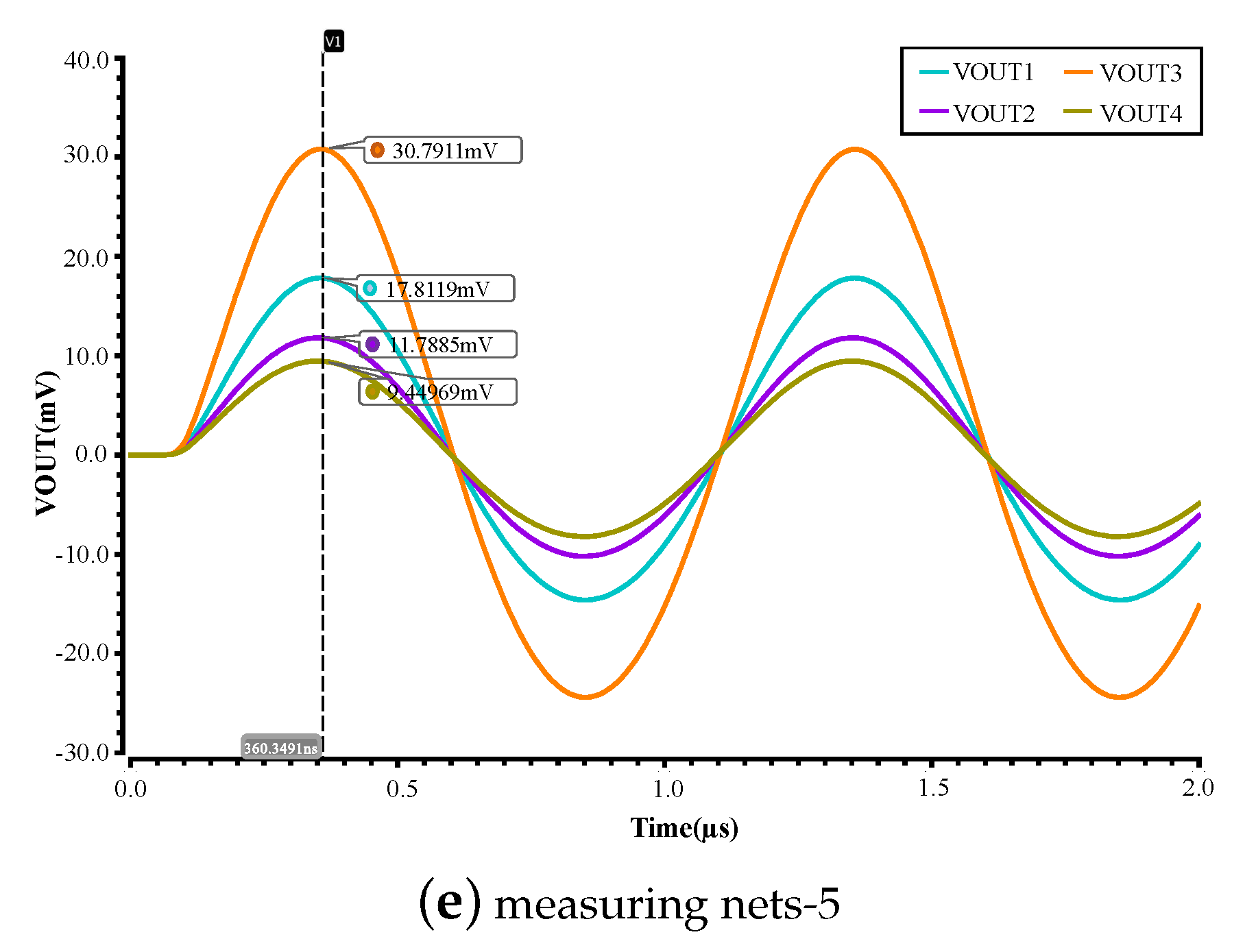
| VOUT1 | 20 | 17.81 | 11.0 |
| VOUT2 | 13.5 | 11.79 | 12.7 |
| VOUT3 | 34 | 30.79 | 9.4 |
| VOUT4 | 10.83 | 9.45 | 12.7 |
| Case | Structure | RMSE(%) | Power | Expected | Working | Configurable | Hardware | |
|---|---|---|---|---|---|---|---|---|
| MLP | of | Dissipation | Area | Frequency | Weight Bits | Cost | ||
| Error Ratio | (mW) | () | (MHz) | (bit) | ||||
| This work | 1 | 2-3-4 | 10.70 | 200 | 1.69 | 1 | 4 | Perceptron chip (low) |
| 2 | 4-3-2 | 10.73 | 192 | 1.56 | ||||
| 3 | 1-2-4 | 10.40 | 131 | 1.17 | ||||
| 4 | 4-2-1 | 10.33 | 118 | 0.96 | ||||
| 5 | 1-3-9 | 10.59 | 223 | 2.73 | ||||
| (Analog-based MLPs) | 6 | 9-3-1 | 10.41 | 219 | 2.17 | |||
| 7 | 7-6-5 | 10.58 | 234 | 3.05 | ||||
| 8 | 12-3-1 | 10.37 | 228 | 2.68 | ||||
| FPGA-based MLPs | [17] | 7-5-6 | - | 241 | - | 100 | 16 | Artix-7 (high) |
| [39] | 12-3-1 | - | 1776 | - | 100 | 24 | Zynq-7000 (high) |
© 2020 by the authors. Licensee MDPI, Basel, Switzerland. This article is an open access article distributed under the terms and conditions of the Creative Commons Attribution (CC BY) license (http://creativecommons.org/licenses/by/4.0/).
Share and Cite
Geng, C.; Sun, Q.; Nakatake, S. Implementation of Analog Perceptron as an Essential Element of Configurable Neural Networks. Sensors 2020, 20, 4222. https://doi.org/10.3390/s20154222
Geng C, Sun Q, Nakatake S. Implementation of Analog Perceptron as an Essential Element of Configurable Neural Networks. Sensors. 2020; 20(15):4222. https://doi.org/10.3390/s20154222
Chicago/Turabian StyleGeng, Chao, Qingji Sun, and Shigetoshi Nakatake. 2020. "Implementation of Analog Perceptron as an Essential Element of Configurable Neural Networks" Sensors 20, no. 15: 4222. https://doi.org/10.3390/s20154222
APA StyleGeng, C., Sun, Q., & Nakatake, S. (2020). Implementation of Analog Perceptron as an Essential Element of Configurable Neural Networks. Sensors, 20(15), 4222. https://doi.org/10.3390/s20154222