Letter

A 1 V 92 dB SNDR 10 kHz Bandwidth Second-Order Asynchronous Delta-Sigma Modulator for Biomedical Signal Processing

Department of Microelectronics, Brno University of Technology (BUT), Technická 3058/10, 61600 Brno, Czech Republic
*
Author to whom correspondence should be addressed.
Sensors 2020, 20(15), 4137; https://doi.org/10.3390/s20154137
Submission received: 30 June 2020 / Revised: 20 July 2020 / Accepted: 23 July 2020 / Published: 25 July 2020

Abstract

:
In this paper, a second-order asynchronous delta-sigma modulator (ADSM) is proposed based on the active-RCintegrators. The ADSM is implemented in the 0.18 μ m CMOS Logic or Mixed-Signal/RF, General Purpose process from the Taiwan Semiconductor Manufacturing Company with a center frequency of 848 kHz at a supply voltage of 1 V with a 92 dB peak signal-to-noise and distortion ratio ( S N D R ), which corresponds to 15 bit resolution. These parameters were achieved in all the endogenous bioelectric signals bandwidth of 10 kHz. The ADSM dissipated 295 μ W and had an area of 0.54 mm 2 . The proposed ADSM with a high resolution, wide bandwidth, and rail-to-rail input voltage range provides the universal solution for endogenous bioelectric signal processing.

1. Introduction

Biomedical electronics have acquired significant attention in healthcare, with a focus on the development of biosensors that enable online monitoring, detection, prevention, and personalized medicine for a variety of chronic and acute diseases. Especially in the last few years, there has been growing interest in the design of biomedical wireless sensors [1,2,3]. Biomedical signals can be subdivided into two major classes: (1) endogenous signals that arise from natural physiological processes and are measured within or on living creatures (e.g., (EOG), electroencephalogram (EEG), electrocardiogram (ECG or EKG), electromyogram (EMG), temperature, blood glucose, etc.) and (2) exogenous signals applied from the outside (generally noninvasively) to measure internal structures and parameters. Endogenous bioelectric signals are invariably small, ranging from single microvolts to over 100 mV. Their bandwidths range from DC to perhaps 10 kHz at most [4,5,6,7]. The voltage and frequency ranges of some common biopotential signals are shown in Figure 1.
A general biomedical system consists of an energy source, a differential amplifier, analog-to-digital conversion (ADC), digital signal preprocessing, and a communication subsystem. The ADC is one of the key building blocks, which enables converting analog signals from biomedical sensors to a digital format that can be easily processed and analyzed. For the design of the ADC, many authors choose the SARarchitecture due to its suitability for low-power and low-voltage requirements [8,9,10,11]. Recently, delta-sigma ( Δ Σ ) ADC has been gaining more and more popularity. Compared to other conversion techniques, Δ Σ ADCs cover the widest conversion region of the resolution-versus-bandwidth plane, providing the most efficient solution to digitize diverse types of signals in many different applications such as biomedical ones [12]. There exist two basic types of Δ Σ modulators: discrete-time (DTDSM) and continuous-time (CTDSM). The DTDSM is more attractive for high-resolution applications due to its higher linearity and accuracy. On the other hand, less stringent amplifier speed specifications are required in CTDSM due to the absence of switches in the active-RC integrator, allowing achieving a higher speed of operation and lower power consumption. The asynchronous Δ Σ modulator (ADSM) can be considered as a special type of CTDSM. ADSM is simple, does not require any clocking, matches well with mainstream CMOS technology, and can operate at low current and supply voltages [13,14,15]. A comparison between DTDSM, CTDSM, and ADSM is shown in Table 1.
In several publications, DTDSMs are used for biomedical signal processing [1,16,17]. There also exists solutions utilizing ADSM [18,19,20]. These ADSM are distinguished by very low power consumption in the order of tens of nanowatts. However, their bandwidth is very low in the order of tens of Hertz. The proposed ADSM covers the full bandwidth of endogenous bioelectric signals up to 10 kHz. The differential input range equals V D D A with a 0.5 V reference level ( V C M ). The proposed ADSM with high resolution, wide bandwidth, and rail-to-rail input voltage range provides the universal solution for endogenous bioelectric signal processing. The circuit not only offers an alternative to the developed CTDSMs and DTDSMs, but it also fills the gap between published ADSMs, which do not allow processing the full spectrum of biomedical signals according to Figure 1 except for those with a very high bandwidth in the order of MHz. An important parameter of ADSM is the center frequency, the calculation of which is part of this work. The following sections provide the details of our approach.

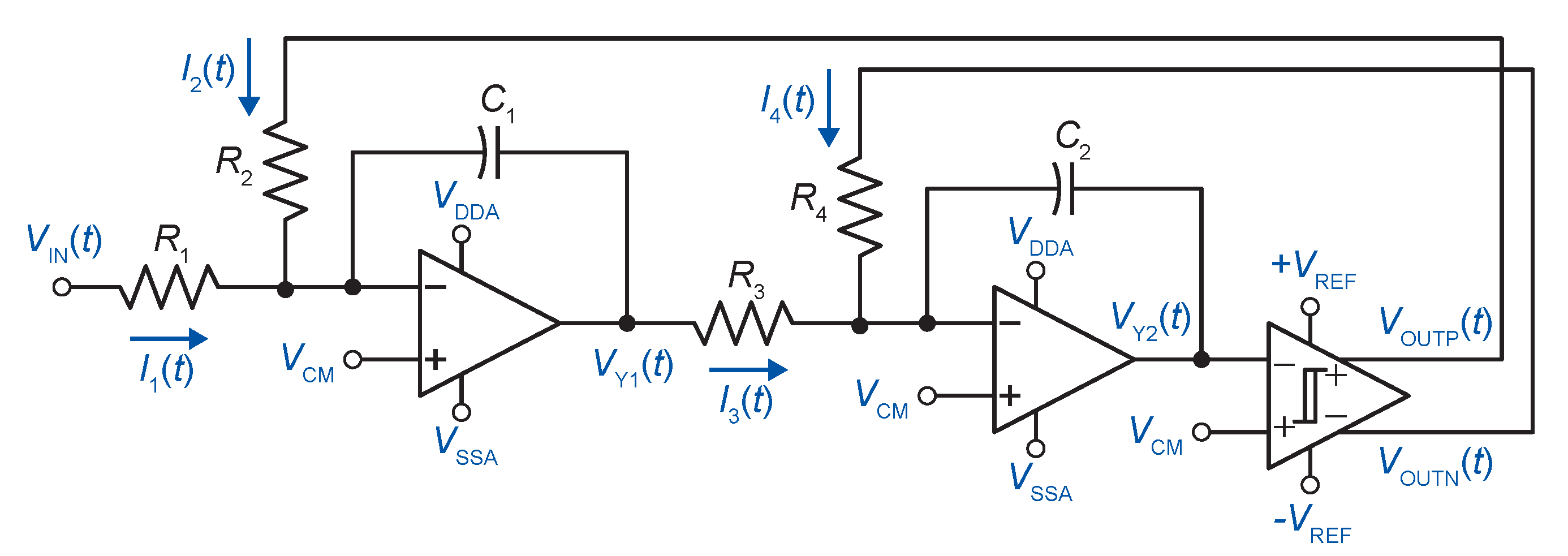
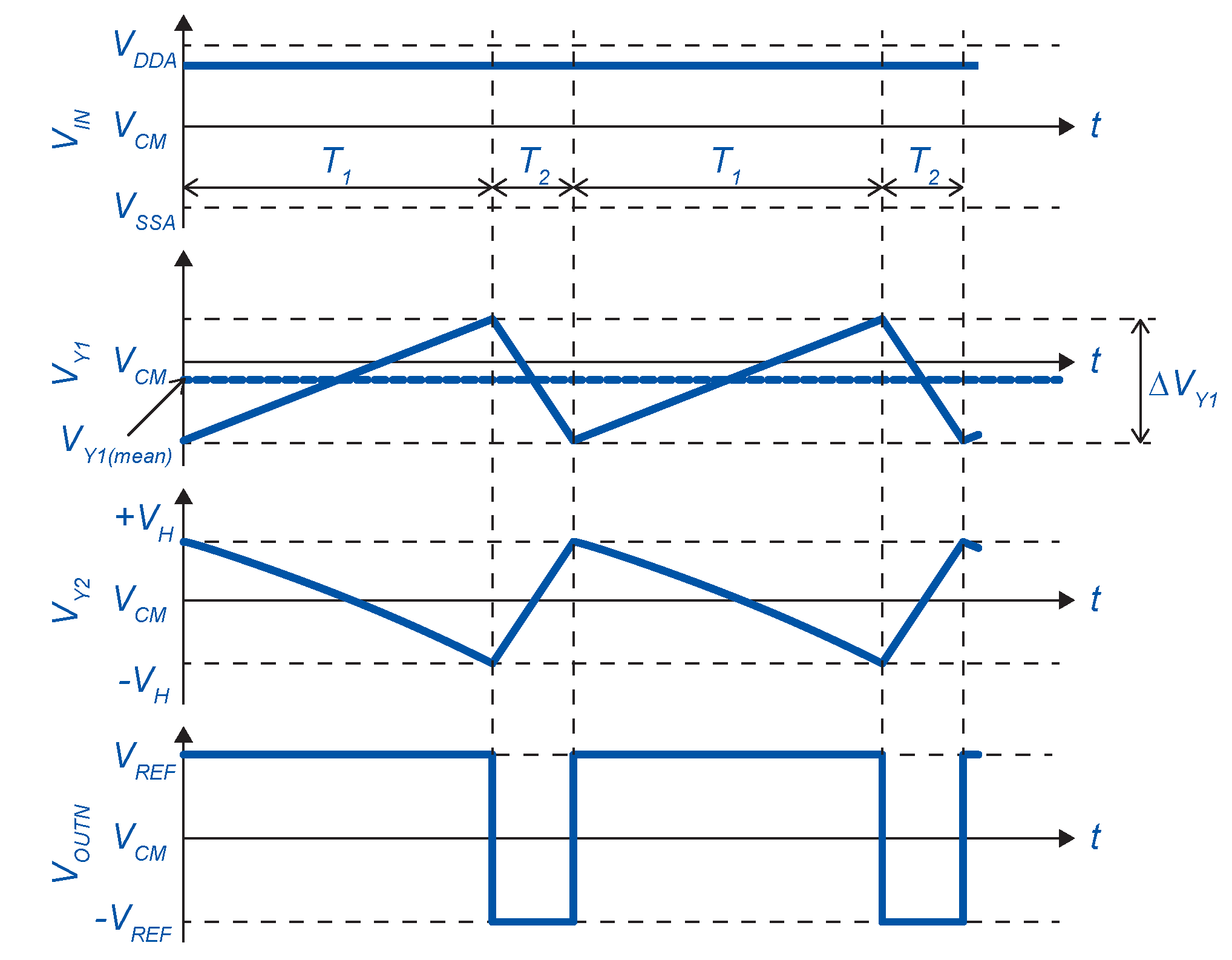
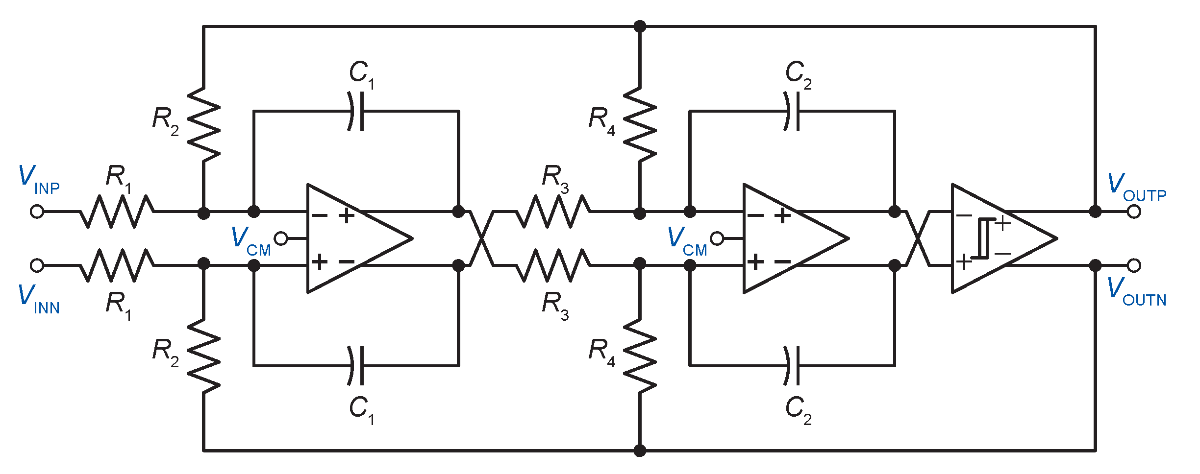
2. Asynchronous Delta-Sigma Modulator

There are two major types of architecture for Δ Σ modulators. The first one is the single-loop and the second the multi-loop architecture. Multi-loop architectures are commonly denoted as cascade or MASH (multi-stage noise shaping). A major drawback of MASH modulators is that precise matching of the analog and digital signal processing paths is required to avoid large errors (quantization noise leakage) caused by integrator gain coefficient variations. Because RC integrators are used in this design, where variations of about 20% in the R C time constant can be expected, the single-loop architecture was chosen in this work. Its stronger ability to achieve high SNDR since it does not suffer from matching errors, which severely affect MASH modulators, is the major advantage in the design.
The block diagram of the second-order ADSM based on the cascade of integrators with distributed feedback (CIFB) topology is shown in Figure 2.
The circuit consists of two integrators and a binary quantizer with hysteresis. The output V O U T P (or V O U T N ) is a pulse width modulated square wave of period T P E R with a pulse width T P W . The duty cycle d is proportional to the amplitude of the input signal (Equation (1)). Moreover, the period T P E R of the asynchronous modulator output signal is modulated by the normalized input voltage V I N (Equation (2)) [21].
d = V I N + 1 2 = T P W T P E R
and:
f 0 f c = 1 V I N 2 a n d v < 1
where f 0 is the output carrier frequency, f c is the maximum value of f 0 , namely the center frequency, and V I N < 1 is the normalized input amplitude.
The center frequency of ADSMs determines the carrier-to-bandwidth ratio ( C B R = f c / ( 2 B ) , where B is the input signal bandwidth), which is the ratio between the center frequency and the signal bandwidth. This ratio is equal to the oversampling ratio ( O S R ) in synchronous delta-sigma modulators. It determines the minimal center frequency required for a certain conversion accuracy. The critical condition can occur when V I N is close to the full scale. The output frequency will decrease, and the high-frequency distortions around the center frequency shift to the low-frequency region. Consequently, distortions can leak into the baseband and adversely affect the modulator linearity for large input amplitudes. Therefore, the center frequency should be set far away from the baseband to avoid these components shifting into the signal baseband, and a high order filter is required to attenuate these out-band components. In order to achieve a high center frequency without degeneration of the linearity, the second-order topology was chosen. To calculate the center frequency of the proposed ADSM, the integrators’ output voltages are expressed as:
V Y 1 ( t ) = I 1 ( t ) C 1 + I 2 ( t ) C 1 t + V C M
V Y 2 ( t ) = I 3 ( t ) C 2 + I 4 ( t ) C 2 t + V C M
where I 1 ( t ) , I 2 ( t ) , I 3 ( t ) , and I 4 ( t ) can be expressed as:
I 1 ( t ) = V I N ( t ) V C M R 1
I 2 ( t ) = V R E F ( t ) V C M R 2
I 3 ( t ) = V Y 1 ( t ) V C M R 3
I 4 ( t ) = V R E F ( t ) V C M R 4
In order to find the center frequency, the timing diagram in Figure 3 is considered, which corresponds to the schematic in Figure 2.
The duty cycle of the ADSM is given by the ratio of rising ( S R E )-to-falling edge ( S F E ) speed. To facilitate the equations, a symmetrical power supply is considered ( V D D A s = V D D A V C M , V C M = 0 V, V S S A s = V S S A V C M , V R E F = V D D A s = V S S A s ; V H L V C M = V H H V C M = V H ). During the T 1 period, the output voltage of the first integrator V Y 1 rises with speed, given by:
S R E 1 = d V Y 1 d t = I 1 + I 2 C 1 = V I N R 2 + V R E F R 1 R 1 R 2 C 1
and the falling edge during T 2 :
S F E 1 = d V Y 1 d t = I 1 + I 2 C 1 = V I N R 2 V R E F R 1 R 1 R 2 C 1
The first integrator output voltage swing is in the range of:
Δ V Y 1 = V Y 1 ( m e a n ) ± V H I 2 I 4
where V H is the comparator threshold voltage.
In order to find V Y 1 ( m e a n ) , we calculate I 3 ( m e a n ) . The duty cycle of the second integrator output V Y 2 is the same as the first one. From Equations (9) and (10), the value of I 3 ( m e a n ) is calculated to meet the duty cycle requirements.
I 3 ( m e a n ) = V Y 1 ( m e a n ) R 3 = V I N R 2 R 1 R 4
For period T 1 , we can write:
T 1 = 2 V H R 1 R 4 C 2 R 1 V R E F V I N R 2
T 2 = 2 V H R 1 R 4 C 2 R 1 V R E F + V I N R 2
The entire period can be expressed as:
T P E R = T 1 + T 2
When a zero input is applied V I N = 0 , the output of the ADSM is a square wave with a duty cycle of 50%. By defining T C as the period of the output signal, it can be calculated as:
T C = T P E R = 2 T 1 = 2 T 2 = 4 V H R 4 C 2 V R E F
Similar to the conventional synchronous CTDSMs, propagation delay is also an issue in ADSMs. The delay of the comparator increases the effective value of hysteresis and negligibly affects the center frequency of the ADSM. Therefore, the impact of the comparator delay, τ , on the center frequency of the proposed ADSM can be given by:
T C = T P E R = 2 T 1 = 2 T 2 = 1 f C = 4 V H R 4 C 2 V R E F + τ
Equation (17) shows that the center frequency f C of the modulator will decrease for a higher delay of the comparator, which degenerates the input bandwidth and linearity of the modulator [20].

3. Transistor Level Realization

In this section, the transistor level implementation of the ADSM will be described. Figure 4 illustrates the circuit diagram of the proposed ADSM. The implemented architecture is fully differential to minimize even-order harmonics, as well as common-mode noise.

3.1. Active-RC Integrator

In the proposed design, the active-RC integrators were used due to simplicity, high linearity, parasitic insensitivity, as well as the overall power consumption. The ideal transfer function of the active-RC integrator is given by:
I n t ( s ) = 1 s R C = k i f s s
where f s is the sampling frequency and k i is the scaling coefficient.
The parameters of the resistors and capacitors were designed to achieve a high center frequency according to Equation (16). The lower limit for R and C is defined by matching consideration and maximum charging current in the case of R. The upper limit for R is set by the allowed thermal noise level, which itself is fixed by the overall dynamic range requirements. Finding optimal R and C was also confirmed by behavioral simulations in MATLAB/Simulink, as well as variations of about 20% in the R C time constant. The R and C values were R 1 = 650 k Ω , R 2 = R 4 = 500 k Ω , R 3 = 357 k Ω , V H = 90 mV, C 1 = C 2 = 2 pF, and I R = 1 μ A. It can be calculated from Equation (16) that f C = 1.39 MHz, and from Equation (11), V Y 1 ( m e a n ) = (0 ± 90) mV. The validity of these results was verified in MATLAB/Simulink and is shown in Figure 5.
As will be seen later, nonidealities such as input parasitic capacitances of the operational amplifier and the delay of the comparator negligibly affect the center frequency of the modulator.

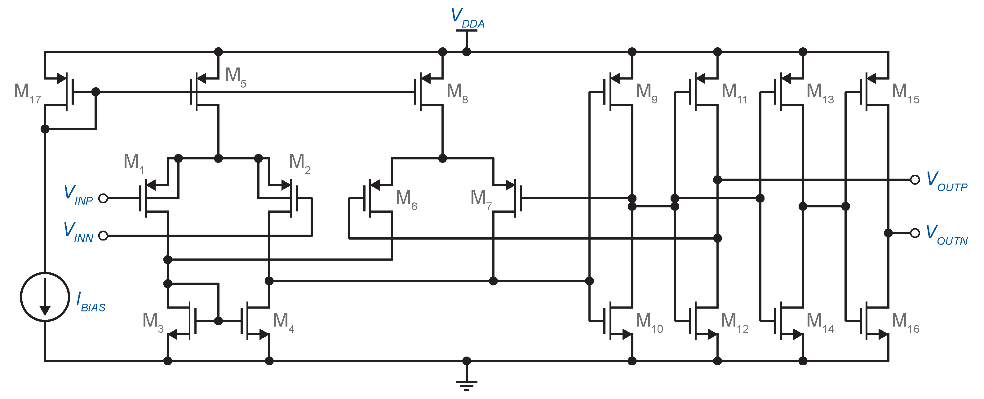
3.2. Class AB Fully Differential Operational Amplifier

The integrators in the ADSM were each implemented using the two-stage, Class A/AB operational amplifier topology shown in Figure 6. This topology combines a simple differential pair as the first stage with a Class A/AB second stage, wherein push-pull operation is implemented using current mirrors [22]. The slew-rate is limited only by the first stage.
S R = I 5 C C 1 + C G 6 + C G 13
The minimum value of the operational amplifier slew-rate can be determined from the falling edge speed of V Y 2 ( S F E 2 ) according to Figure 3. The input parasitic capacitance of the comparator ( C c o m p ) should be included in the calculations. Thus,
S F E 2 = d V Y 2 d t = I 3 + I 4 C 2 + C c o m p = V Y 1 R 4 + V R E F R 3 R 3 R 4 ( C 2 + C c o m p )
The use of PMOS input transistors makes it possible to avoid the body effect. The compensation network is comprised of capacitor C C and resistor R M , which cancels the right half plane zero.
For the detection of the common-mode output voltage, two equal resistors were used ( R C M = 500 k Ω ). The voltage between the two resistors is subtracted from the desired common-mode output voltage, V C M , and scaled by the one-stage differential amplifier that consists of source-coupled pair M 15 –M 16 , diode-connected loads M 17 and M 18 , and tail current source M 19 . The main reason for using this solution is that the input to the common-mode sense amplifier (gate of M 15 ) is almost constant. Therefore, this CMFB solution does not limit the operational amplifier output voltage swing. Table 2 sums up the simulated parameters of the operational amplifier used in the integrators.

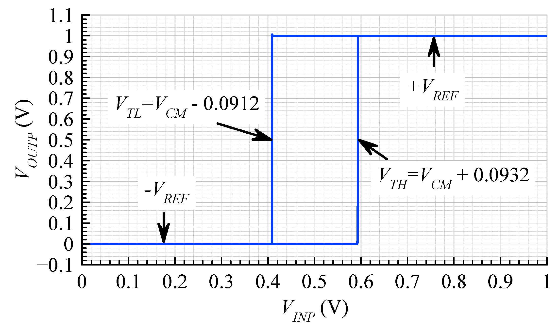
3.3. Comparator with Hysteresis

The schematic of a comparator using the internal positive feedback circuit is given in Figure 7. The comparator consists of a differential pair (M 1 –M 2 ) with output inverters in order to to achieve reasonable voltage swings, output resistance, and differential output. A second, smaller differential pair, M 6 –M 7 , unbalances the input differential pair. The inputs of the second differential pair are tied to the output signals in such a way as to introduce positive feedback and, hence, hysteresis.
If M 1 and M 2 are operating in strong inversion, the amount of hysteresis V T H V T L can be calculated using [23]:
V T H V T L = 2 ( I D 3 + I D 11 I D 3 I D 11 ) μ C O X ( W / L ) 1
If M 1 and M 2 are operating in weak inversion,
V T H V T L = 4 n U T tanh 1 ( I D 11 / I D 3 )
Assume that the gate of M 1 ( V I N P ) is tied to V D D A . With the input of M 2 ( V I N N ) much less than V D D A , M 1 is off and M 2 on, and V O U T P is at V D D A and V O U T N at V S S A , thus turning on M 7 and turning off M 4 and M 6 . In this state, no current flows through the differential pairs. As the voltage at the V I N P input decreases toward the threshold point (Equations (21) or (22)), some of I D 5 begins to flow through M 1 and M 3 , and simultaneously, some of the hysteresis bias current I D 8 begins to flow through M 4 . This continues until the point where the current through M 1 equals the current I D 8 . Just beyond this point, the comparator switches its state.
Figure 8 shows the voltage transfer characteristic of the comparator. The hysteresis bias current I D 8 was 6.8 μ A, and the input bias current I D 5 was 10 μ A. The output high-to-low threshold, V T L , was simulated as −90 mV. The output low-to-high threshold, V T H , was simulated as +90 mV. The amount of hysteresis was 180 mV. Simulated parameters of the comparator circuit are given in Table 3.
According to parameters mentioned in Table 2 and Table 3, the center frequency was recalculated to f C = 857 kHz.

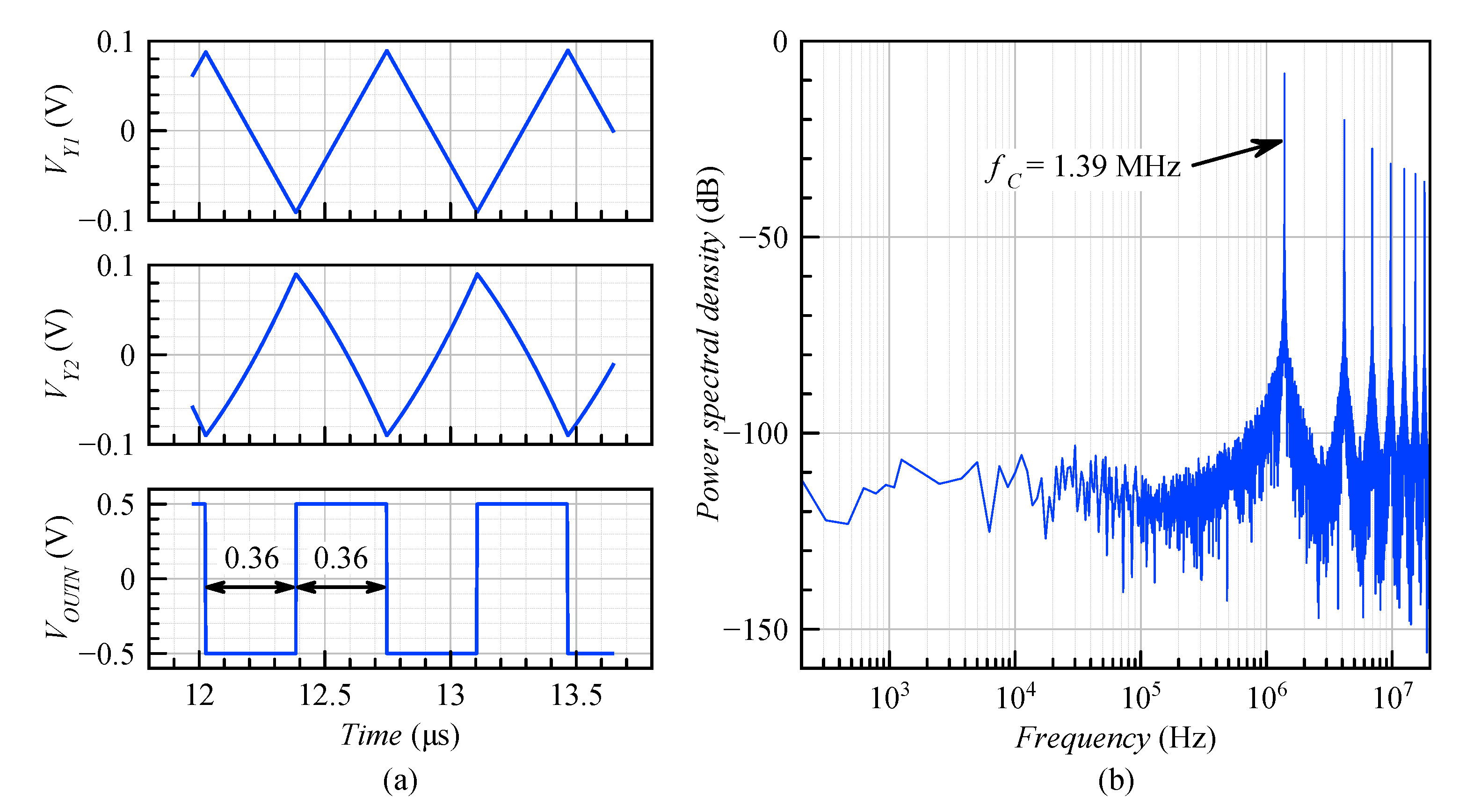
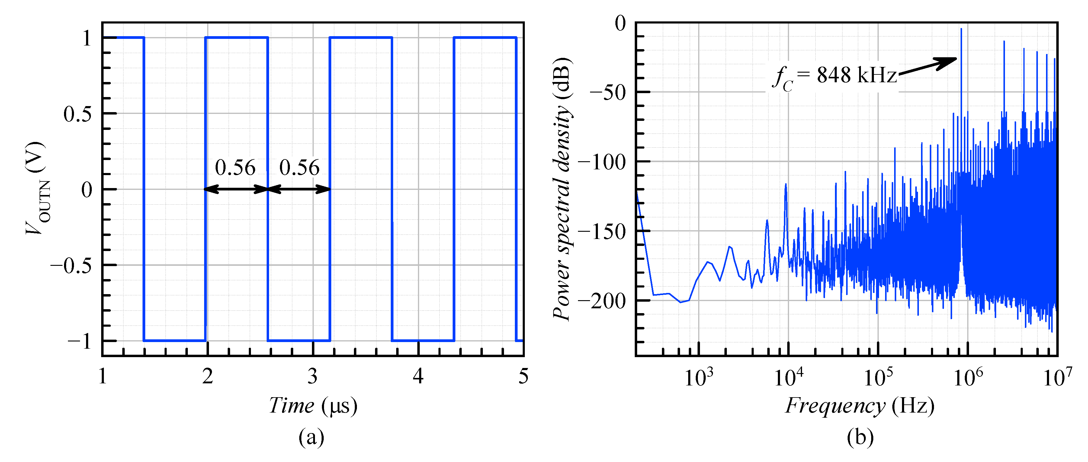
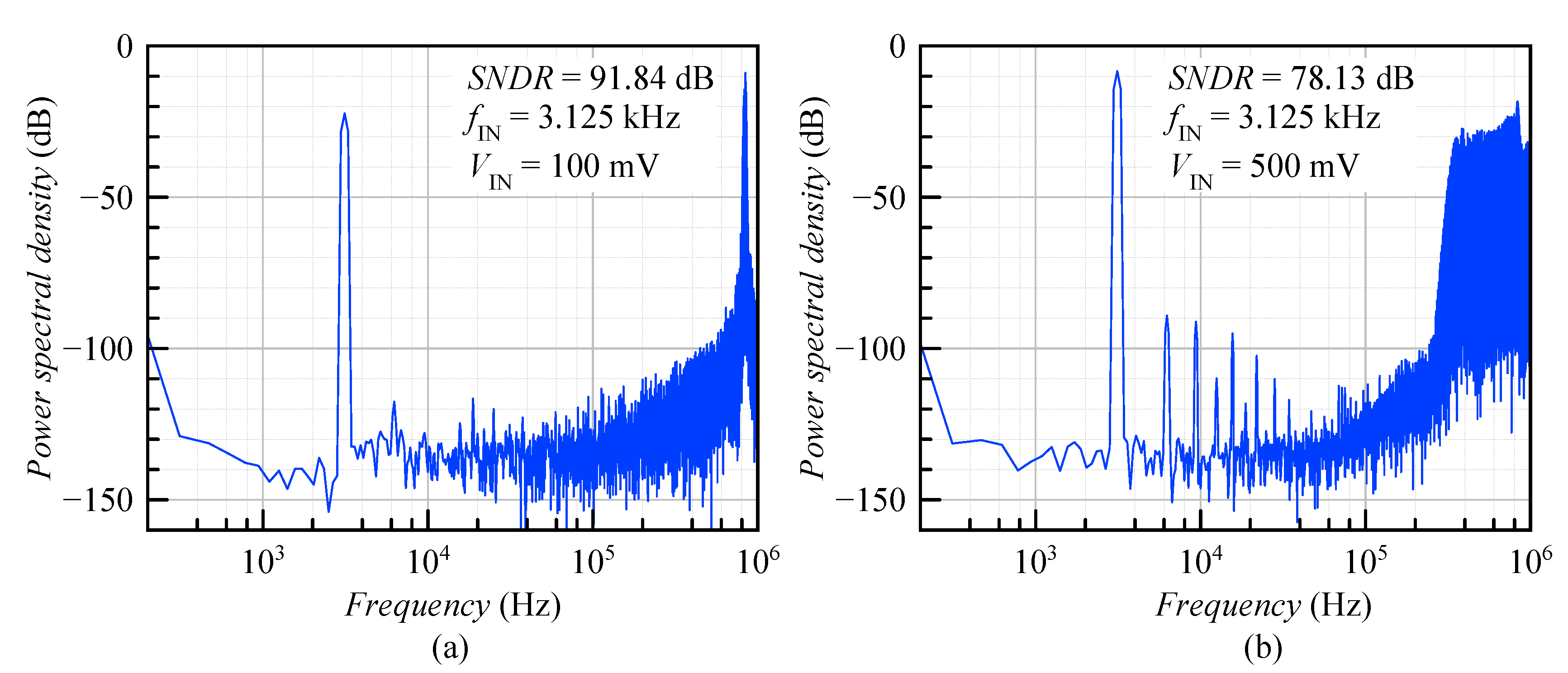
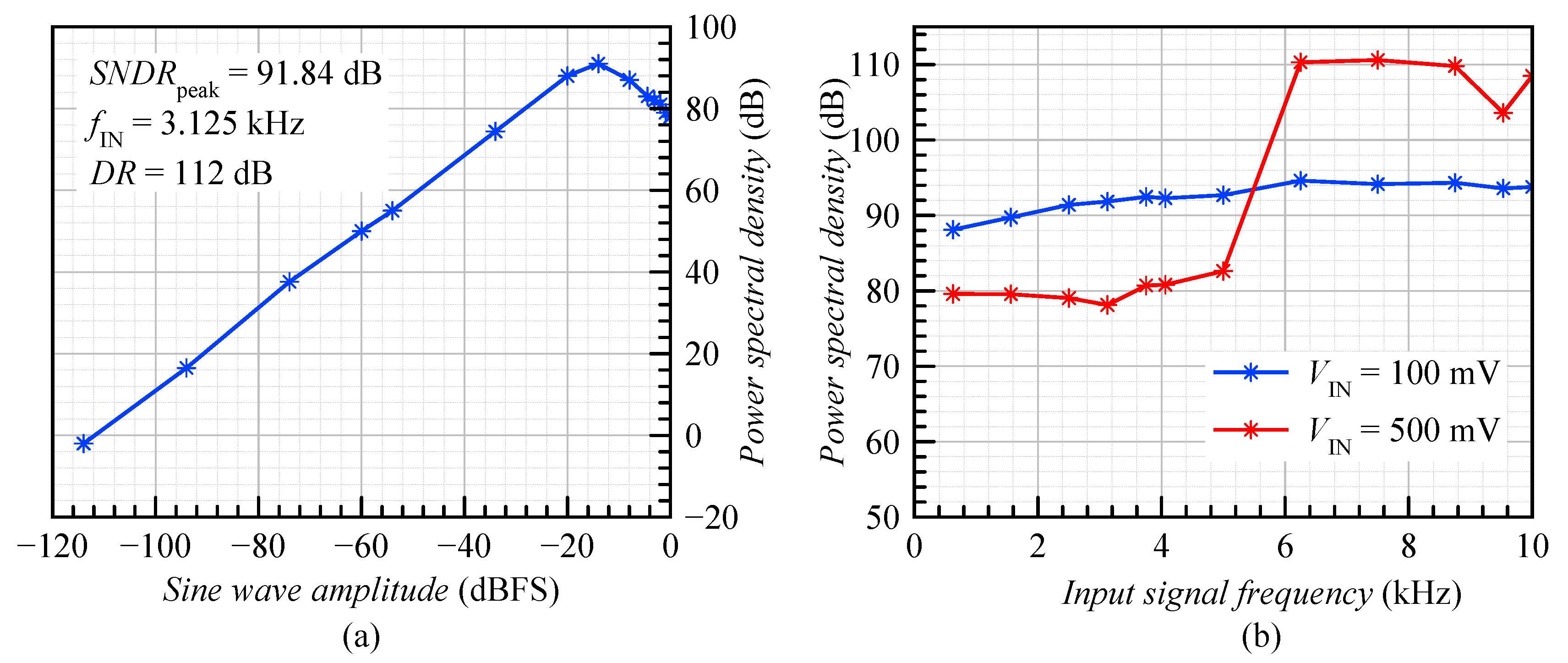
4. Simulation Results

The ADSM was designed utilizing the 0.18 μ m CMOS Logic or Mixed-Signal/RF, General Purpose process from the Taiwan Semiconductor Manufacturing Company. The circuit was designed for V D D = 1 V and I B I A S = 2.5 μ A. After completion of the layout design, its parasitic extraction was performed to find the parasitic resistances and capacitances corresponding to the designed devices and interconnects. After parasitic extraction, all simulations were performed using the Spectre simulator on the Cadence platform. The layout of the ADSM is shown in Figure 9. The layout size is 350 × 155 μ m.
The ADSM output bitstream can be recovered by applying an ideal low pass filter with a cut-off frequency at the signal bandwidth. When ADSMs are used in A/D data conversion, a decoding circuit is required. The simplest one is the sample and hold circuit with a high sampling frequency. The time domain waveforms of the output signal V O U T N for V I N = 0 V and the corresponding frequency spectrum are shown in Figure 10. The limit cycle frequency of the post-layout model of the ADSM was equal to 848 kHz and was very close to the calculated value in Section 3.3 ( f C = 857 kHz). The small difference was caused by the parasitic capacitances and resistances extracted from the layout.
Figure 11 shows the simulated spectrum of the ADSM for a sinusoidal input signal with an amplitude of (a) 100 mV (20% modulation depth) and (b) 500 mV (100% modulation depth). The corresponding spectra were obtained by applying a signal at f I N f B a n d w i d t h / 3 to include at least the second and third harmonic inside the band of interest. Due to this reason, the input frequency was set to 3.125 kHz, and then the third harmonic component was located in the 10 kHz bandwidth. The achieved S N D R was (a) 91.84 dB and (b) 78.13 dB. In the second case, the significant S N D R reduction was caused by higher harmonic tones.
Figure 12a shows the simulated dynamic range ( D R ) with respect to the amplitude of the input signal with a frequency of both 3.125 kHz and 6.25 kHz. As the sine wave amplitude increased, the S N D R increased to reach the peak of 91.84 dB at −14 dBFS, and then dropped to 78.13 dB at 0 dBFS.
Figure 12b shows the S N D R vs. input signal frequency with an amplitude of both 100 mV and 500 mV. In the case of the input sine wave amplitude of 100 mV, the S N D R was above 88 dB for all frequencies up to the 10 kHz bandwidth. In the second case, the S N D R dropped from 110 dB to below 80 dB at frequencies smaller than 5 kHz ( f B a n d w i d t h / 2 ). This was because the second harmonic penetrated into the baseband and significantly reduced the S N D R . The dynamic range was equal to 112 dB.
Table 4 presents a comparison of the proposed ADSM with other DSMs, which are capable of processing endogenous bioelectric signals in the full frequency range. Two figures of merit ( F O M 1 , F O M 2 ) are defined in Equations (23) and (24) for a better comparison. The first one emphasizes power consumption, whereas the second one emphasizes resolution. A better performance of DSMs is indicated by smaller F O M 1 and larger F O M 2 values.
F O M 1 = P c o n s 2 E N O B 2 B W
F O M 2 = D R + 10 log B W P c o n s
As can be concluded from Table 4, the proposed modulator offers a high S N D R and the best values of F O M 2 . Higher power consumption could be further improved utilizing a one-stage operational amplifier with much lower power consumption. The most attractive feature of ADSMs is the simple circuit architecture and clock-less operation. This feature can be very useful in applications in wireless sensors, where a decoding circuit (e.g., time-to-digital converter) is realized outside the integrated circuit.

5. Conclusions

This paper presents a second-order ADSM utilizing active-RC integrators. The circuit was designed in the 0.18 μ m CMOS Logic or Mixed-Signal/RF, General Purpose process from the Taiwan Semiconductor Manufacturing Company. Post-layout simulation was performed using the Spectre simulator on the Cadence platform. The proposed ADSM with a center frequency of 828 kHz achieves a 92 dB peak S N D R , while having a Walden F O M of 0.45 pJ/step and a Shreirer F O M of 187 dB. These parameters together with a bandwidth of 10 kHz provide the universal solution for endogenous bioelectric signal processing. The overall power consumption is 295 μ W, while the chip area corresponds only to 0.54 mm 2 .

Author Contributions

Conceptualization, V.K. and L.F.; methodology, V.K. and L.F.; validation, V.K., R.P., L.F. and J.H.; formal analysis, V.K. and J.H.; investigation, V.K., L.F., and R.P.; writing, original draft preparation, V.K.; writing, review and editing, V.K., L.F., and J.H. All authors have read and agreed to the published version of the manuscript.

Funding

The research described in this paper was supported by the Czech Science Foundation Project No. 19-22248S.

Acknowledgments

For this research, the infrastructure of the SIX Center was used. Cadence software was used with support through the Cadence Academic Network.

Conflicts of Interest

The authors declare no conflict of interest.

Abbreviations

The following abbreviations are used in this manuscript:
ADCAnalog-to-digital converter
ADSMAsynchronous delta-sigma modulator
C B R Carrier-to-bandwidth ratio
CIFBCascade of integrators with distributed feedback
CTDSMContinuous-time delta-sigma modulator
D R Dynamic Range
DTDSMDiscrete-time delta-sigma modulator
F O M Figure-of-merit
MASHMulti-stage noise shaping
S N D R Signal-to-noise and distortion ratio

References

  1. Kledrowetz, V.; Prokop, R.; Fujcik, L.; Pavlik, M.; Háze, J. Low-power ASIC suitable for miniaturized wireless EMG systems. J. Electr. Eng. 2019, 70, 393–399. [Google Scholar] [CrossRef] [Green Version]
  2. Magno, M.; Benini, L.; Spagnol, C.; Popovici, E. Wearable low power dry surface wireless sensor node for healthcare monitoring application. In Proceedings of the 2013 IEEE 9th International Conference on Wireless and Mobile Computing, Networking and Communications (WiMob), Lyon, France, 7–9 October 2013; pp. 189–195. [Google Scholar]
  3. Vinod, A.P.; Da, C.Y. An integrated surface EMG data acquisition system for sports medicine applications. In Proceedings of the 2013 7th International Symposium on Medical Information and Communication Technology (ISMICT), Tokyo, Japan, 6–8 March 2013; pp. 98–102. [Google Scholar]
  4. Northrop, R.B. Analysis and Application of Analog Electronic Circuits to Biomedical Instrumentation (Biomedical Engineering); CRC Press, Inc.: Boca Raton, FL, USA, 2004. [Google Scholar]
  5. Webster, J. Medical Instrumentation: Application and Design; John Wiley & Sons: Hoboken, NJ, USA, 2010. [Google Scholar]
  6. Prutchi, D.; Norris, M. Design and Development of Medical Electronic Instrumentation; Wiley Online Library: Hoboken, NJ, USA, 2005. [Google Scholar]
  7. Delgado, J.M. Electrodes for extracellular recording and stimulation. In Electrophysiological Methods; Elsevier: Amsterdam, The Netherlands, 1964; pp. 88–143. [Google Scholar]
  8. Rodríguez-Pérez, A.; Delgado-Restituto, M.; Medeiro, F. Power Efficient ADCs for Biomedical Signal Acquisition. Available online: http://citeseerx.ist.psu.edu/viewdoc/download?doi=10.1.1.936.432&rep=rep1&type=pdf (accessed on 25 July 2020).
  9. Zou, X.; Xu, X.; Yao, L.; Lian, Y. A 1-V 450-nW Fully Integrated Programmable Biomedical Sensor Interface Chip. IEEE J. Solid-State Circuits 2009, 44, 1067–1077. [Google Scholar] [CrossRef]
  10. Sundarasaradula, Y.; Constandinou, T.G.; Thanachayanont, A. A 6-bit, two-step, successive approximation logarithmic ADC for biomedical applications. In Proceedings of the 2016 IEEE International Conference on Electronics, Circuits and Systems (ICECS), Monte Carlo, Monaco, 11–14 December 2016; pp. 25–28. [Google Scholar]
  11. Mesgarani, A.; Ay, S.U. A low voltage, energy efficient supply boosted SAR ADC for biomedical applications. In Proceedings of the 2011 IEEE Biomedical Circuits and Systems Conference (BioCAS), San Diego, CA, USA, 10–12 November 2011; pp. 401–404. [Google Scholar]
  12. De la Rosa, J.M.; Schreier, R.; Pun, K.; Pavan, S. Next-Generation Delta-Sigma Converters: Trends and Perspectives. IEEE J. Emerg. Sel. Top. Circuits Syst. 2015, 5, 484–499. [Google Scholar] [CrossRef]
  13. Ouzounov, S.; Engel, R.; Hegt, J.A.; van der Weide, G.; van Roermund, A.H.M. Analysis and design of high-performance asynchronous sigma-delta Modulators with a binary quantizer. IEEE J. Solid-State Circuits 2006, 41, 588–596. [Google Scholar] [CrossRef]
  14. Dazhi, W.; Vaibhav, G.; Harris, J.G. An asynchronous delta-sigma converter implementation. In Proceedings of the 2006 IEEE International Symposium on Circuits and Systems, Island of Kos, Greece, 21–24 May 2006; p. 4. [Google Scholar]
  15. Daniels, J.; Dehaene, W.; Steyaert, M.S.; Wiesbauer, A. A/D conversion using asynchronous delta-sigma modulation and time-to-digital conversion. IEEE Trans. Circuits Syst. I Regul. Pap. 2010, 57, 2404–2412. [Google Scholar] [CrossRef]
  16. Lee, J.; Song, S.; Roh, J. A 103 dB DR Fourth-Order Delta-Sigma Modulator for Sensor Applications. Electronics 2019, 8, 1093. [Google Scholar] [CrossRef] [Green Version]
  17. Sohel, A.; al Khadir, A.; Naaz, M.; Najeeb, A. A 1.8V 204.8-μW 12-Bit Fourth Order Active Passive ΣΔ Modulator for Biomedical Applications. In Proceedings of the 2019 Devices for Integrated Circuit (DevIC), Kalyani, India, 23–24 March 2019; pp. 124–127. [Google Scholar]
  18. Ferreira, L.H.C.; Sonkusale, S.R. A 0.25-V 28-nW 58-dB Dynamic Range Asynchronous Delta Sigma Modulator in 130-nm Digital CMOS Process. IEEE Trans. Very Large Scale Integr. (VLSI) Syst. 2015, 23, 926–934. [Google Scholar] [CrossRef]
  19. Kulej, T.; Khateb, F.; Ferreira, L.H.C. A 0.3-V 37-nW 53-dB SNDR Asynchronous Delta–Sigma Modulator in 0.18-μm CMOS. IEEE Trans. Large Scale Integr. (VLSI) Syst. 2019, 27, 316–325. [Google Scholar] [CrossRef]
  20. Akbari, M.; Hashemipour, O.; Moradi, F. Design and analysis of an ultra-low-power second-order asynchronous delta–sigma modulator. Circuits Syst. Signal Process. 2017, 36, 4919–4936. [Google Scholar] [CrossRef]
  21. Roza, E. Analog-to-digital conversion via duty-cycle modulation. IEEE Trans. Circuits Syst. II Analog Digit. Signal Process. 1997, 44, 907–914. [Google Scholar] [CrossRef]
  22. Rabii, S.; Wooley, B.A. A 1.8-V digital-audio sigma-delta modulator in 0.8-/spl mu/m CMOS. IEEE J. Solid-State Circuits 1997, 32, 783–796. [Google Scholar] [CrossRef]
  23. Furth, P.M.; Tsen, Y.C.; Kulkarni, V.B.; Raju, T.K.P.H. On the design of low-power CMOS comparators with programmable hysteresis. In Proceedings of the 2010 53rd IEEE International Midwest Symposium on Circuits and Systems, Seattle, WA, USA, 1–4 August 2010; IEEE: Piscataway, NJ, USA, 2010; pp. 1077–1080. [Google Scholar]
  24. Yoon, Y.; Choi, D.; Roh, J. A 0.4 V 63 μW 76.1 dB SNDR 20 kHz Bandwidth Delta-Sigma Modulator Using a Hybrid Switching Integrator. IEEE J. Solid-State Circuits 2015, 50, 2342–2352. [Google Scholar] [CrossRef]
  25. Leow, Y.H.; Tang, H.; Sun, Z.C.; Siek, L. A 1 V 103 dB 3rd-Order Audio Continuous-Time ΔΣ ADC with Enhanced Noise Shaping in 65 nm CMOS. IEEE J. Solid-State Circuits 2016, 51, 2625–2638. [Google Scholar] [CrossRef]
  26. Liao, S.; Wu, J. A 1 V 175 μW 94.6 dB SNDR 25 kHz bandwidth delta-sigma modulator using segmented integration techniques. In Proceedings of the 2018 IEEE Custom Integrated Circuits Conference (CICC), San Diego, CA, USA, 8–11 April 2018; pp. 1–4. [Google Scholar]
  27. Michel, F.; Steyaert, M.S.J. A 250 mV 7.5 μW 61 dB SNDR SC ΔΣ Modulator Using Near-Threshold-Voltage-Biased Inverter Amplifiers in 130 nm CMOS. IEEE J. Solid-State Circuits 2012, 47, 709–721. [Google Scholar] [CrossRef]
Figure 1. Voltage and frequency ranges of some common biopotential signals.
Sensors 20 04137 g001
Figure 2. Simplified schematic of the second-order ADSM with the CIFB topology.
Sensors 20 04137 g002
Figure 3. Timing diagram of the asynchronous sigma delta modulator with a constant input.
Sensors 20 04137 g003
Figure 4. Proposed second-order asynchronous delta–sigma modulator.
Sensors 20 04137 g004
Figure 5. MATLAB model simulation results: (a) timing diagram and (b) frequency spectrum of the ADSM for V I N = 0 V.
Sensors 20 04137 g005
Figure 6. Circuit schematic of the two-stage Class A/AB operational amplifier.
Sensors 20 04137 g006
Figure 7. Comparator with hysteresis using an unbalanced differential pair.
Sensors 20 04137 g007
Figure 8. Simulated DC transfer characteristic of the comparator.
Sensors 20 04137 g008
Figure 9. Layout of the proposed ADSM.
Sensors 20 04137 g009
Figure 10. Post-layout simulation results: (a) timing diagram and (b) frequency spectrum of the ADSM for V I N = 0 V.
Sensors 20 04137 g010
Figure 11. PSDof the ADSM for the sinusoidal input signal with an amplitude of (a) V I N = 100 mV and (b) V I N = 500 mV.
Sensors 20 04137 g011
Figure 12. Plot of the S N D R vs. the (a) input sine wave amplitude and (b) input signal frequency.
Sensors 20 04137 g012
Table 1. Comparison between DTDSM, CTDSM, and ADSM.
DTDSMCTDSMADSM
+ Synchronous system+ Synchronous system+ Immunity to clock jitter
+ High resolution+ Implicit antialiasing filter+ Implicit antialiasing filter
+ Highly linear SC integrator+ Higher sampling frequency+ Simple circuit
+ Accurately defined integrator+ Relaxed operational amplifier+ Relaxed OpAmp
gains and transfer functionspeed requirementsspeed requirements
+ Low sensitivity to clock jitter+ Higher conversion speed+ Higher conversion speed
and excess loop delay+ Low power+ Low power
+ Low sensitivity to DAC settling time + Do not require a clock
- Low conversion speed- Sensitivity to clock jitter- Complex decoding scheme
- Required pre-antialiasing filter- Excess loop delay- Lack of noise shaping
- Required non-overlapping- Lower resolution- Lower resolution
clock generator
Table 2. Simulated parameters for the operational amplifier ( C L = 3 pF).
ParameterConditionValue
Hysteresis V T H = V T L 90 mV
Time delay C L = 3 pF 50 ns
Slew-rate C L = 3 pF 42 V/ μ s
Power consumptionduty cycle = 50%5 μ W
Input capacitance 0.4 pF
I B I A S 2.5 μ A
Table 3. Simulated parameters for the comparator.
ParameterConditionValue
Hysteresis V T H = V T L 90 mV
Time delay C L = 3 pF 50 ns
Slew-rate C L = 3 pF 42 V/ μ s
Power consumptionduty cycle = 50%5 μ W
Input capacitance 0.4 pF
I B I A S 2.5 μ A
Table 4. Specifications of the proposed ADSM in comparison with other DSMs.
ParameterThis Work[24] 2015[25] 2016[26] 2018[27] 2012
Technology180 nm130 nm65 nm65 nm130 nm
TopologyADSMDTDSMCTDSMDTDSMDTDSM
Order2333 (2-1 MASH)3
Quantizer1 bit1 bit5 bit1 bit1 bit
Supply voltage1 V0.4 V1 V1 V0.25 V
Modulator frequency848 kHz3.2 MHz6.4 MHz5 MHz1.4 MHz
Bandwidth10 kHz20 kHz25 kHz25 kHz10 kHz
Peak S N D R 92 dB76.1 dB95.2 dB94.6 dB61 dB
Dynamic range112 dB82 dB103 dB98.5 dB≅ 58 dB
Power consumption290 μ W63 μ W800 μ W175 μ W7.5 μ W
Area0.54 mm 2 0.33 mm 2 0.256 mm 2 0.384 mm 2 0.3375 mm 2
F O M 1 0.45 pJ/step0.31 pJ/step0.34 pJ/step0.079 pJ/step0.41 pJ/step
F O M 2 187 dB167 dB177.9 dB176.2 dB-

