Floating-Gate MOS Transistor with Dynamic Biasing as a Radiation Sensor


Abstract
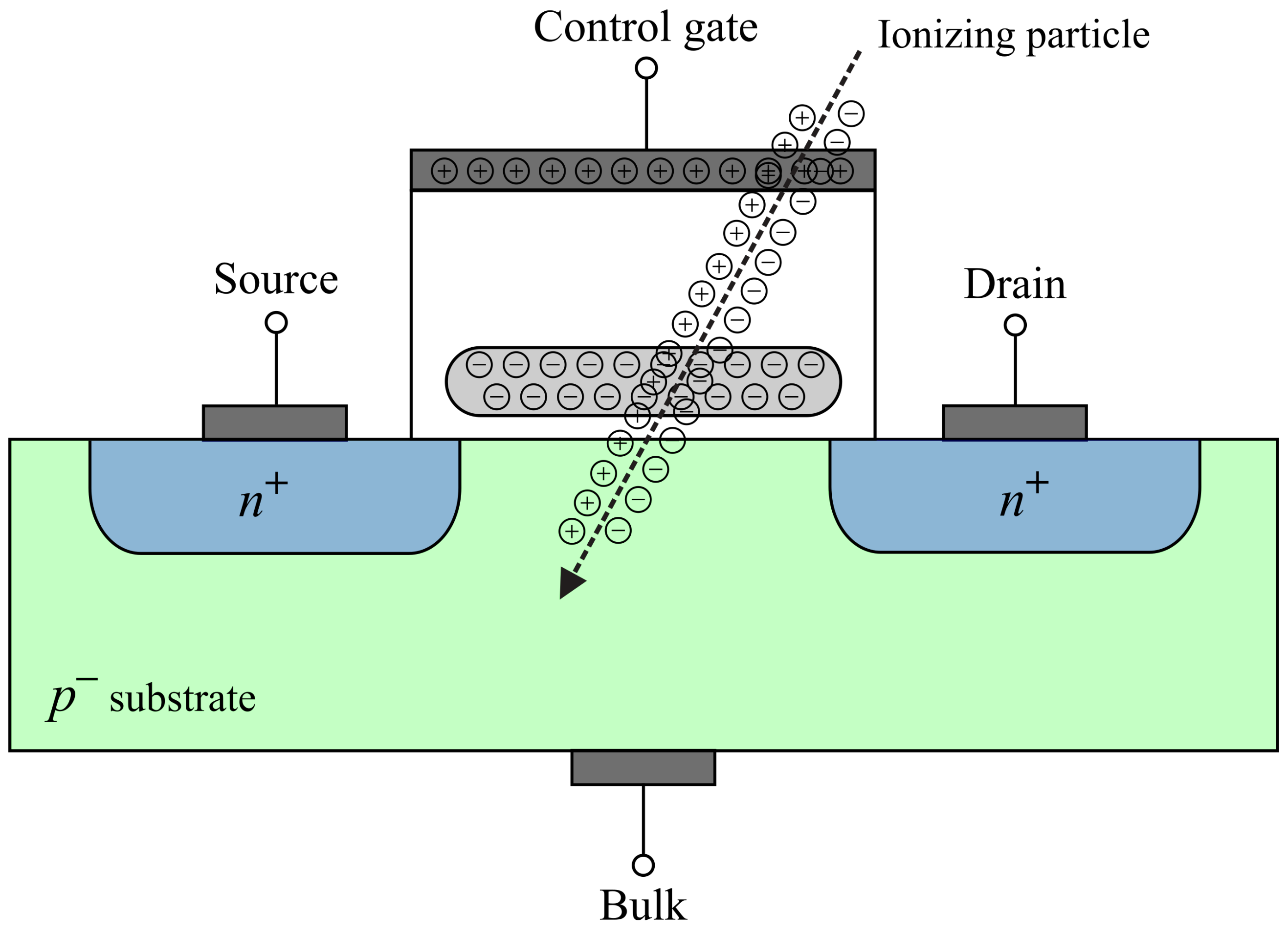
1. Introduction
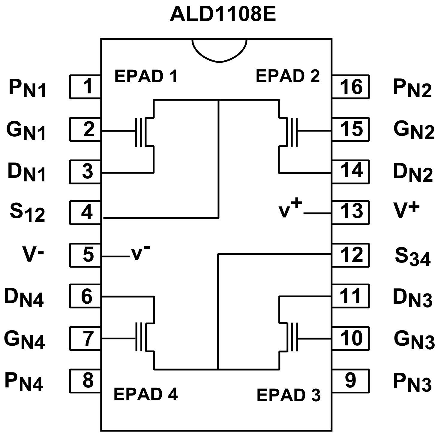
Electrically Programmable Analog Device
2. Materials and Methods
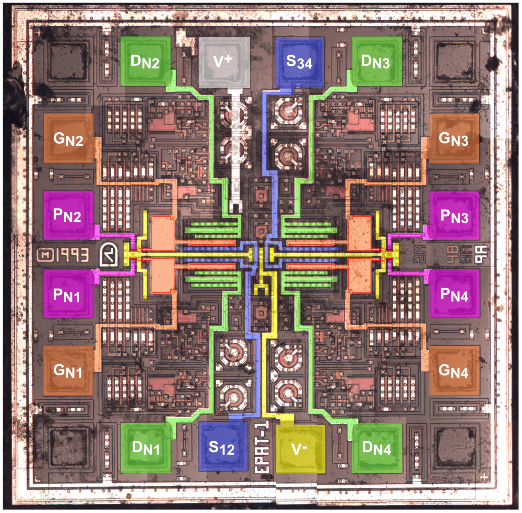
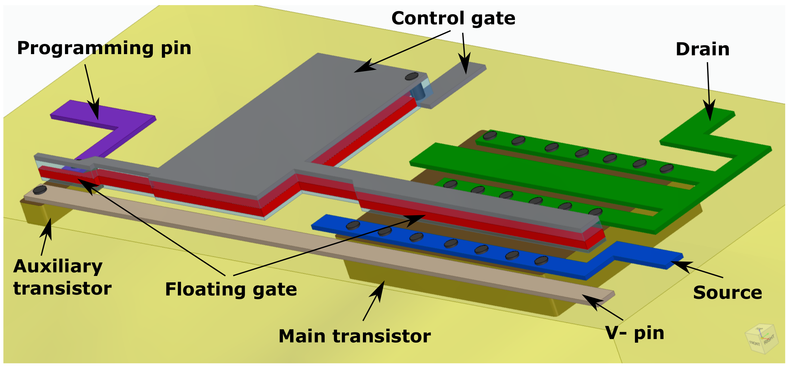
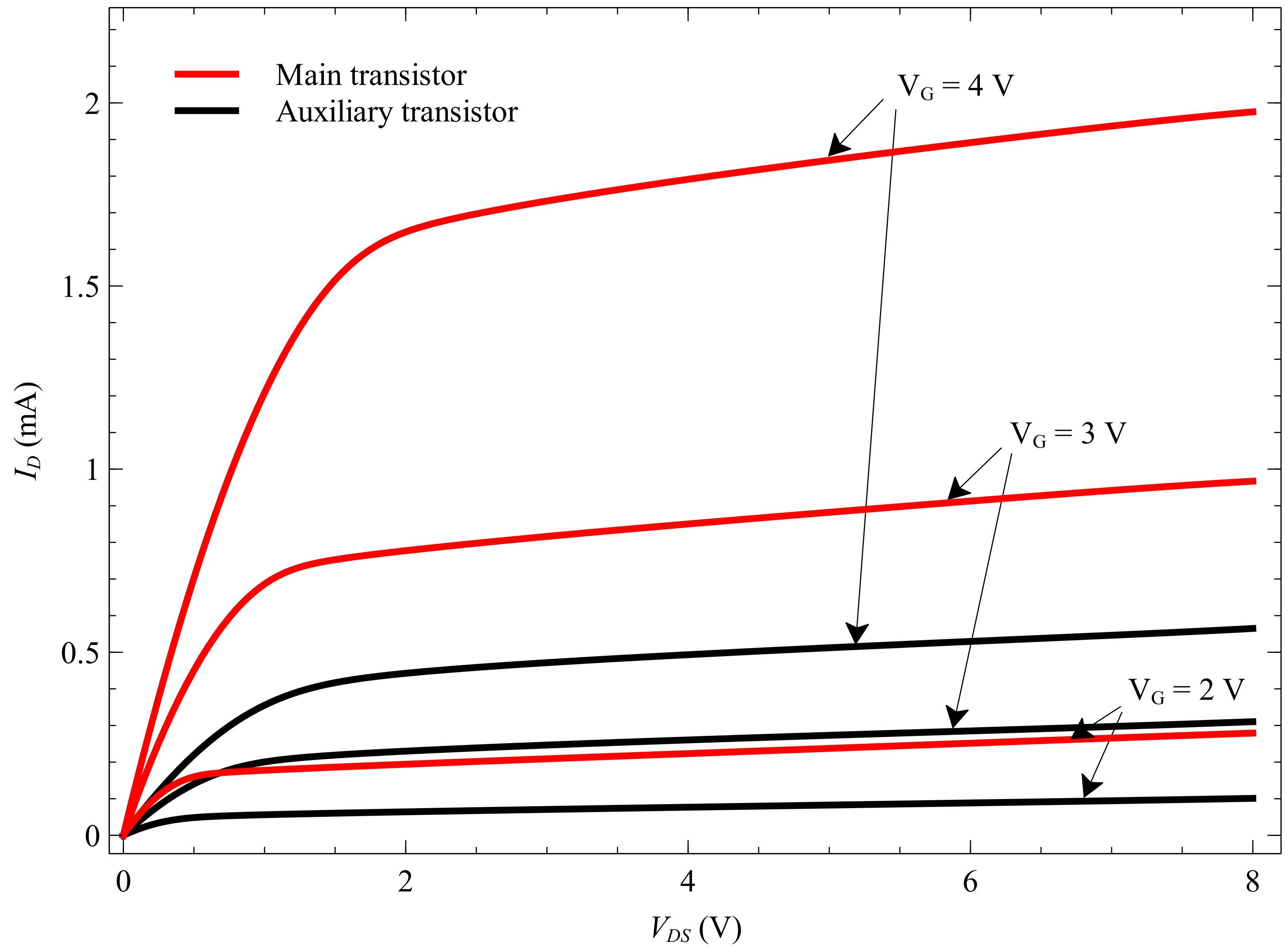
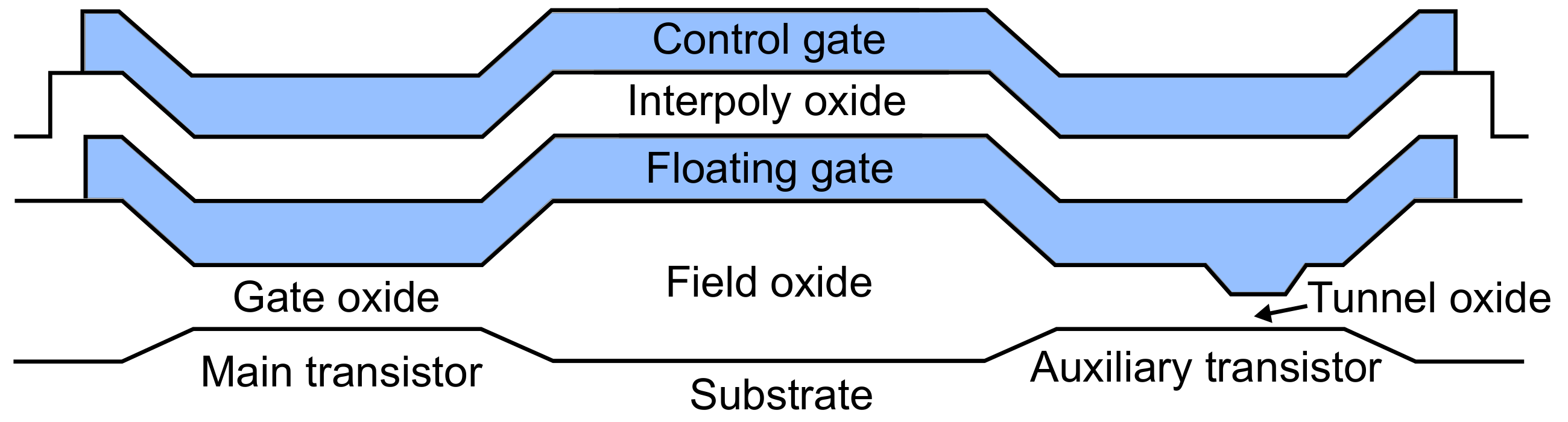
2.1. Reverse Engineering of Epad
2.2. Dynamic Biasing
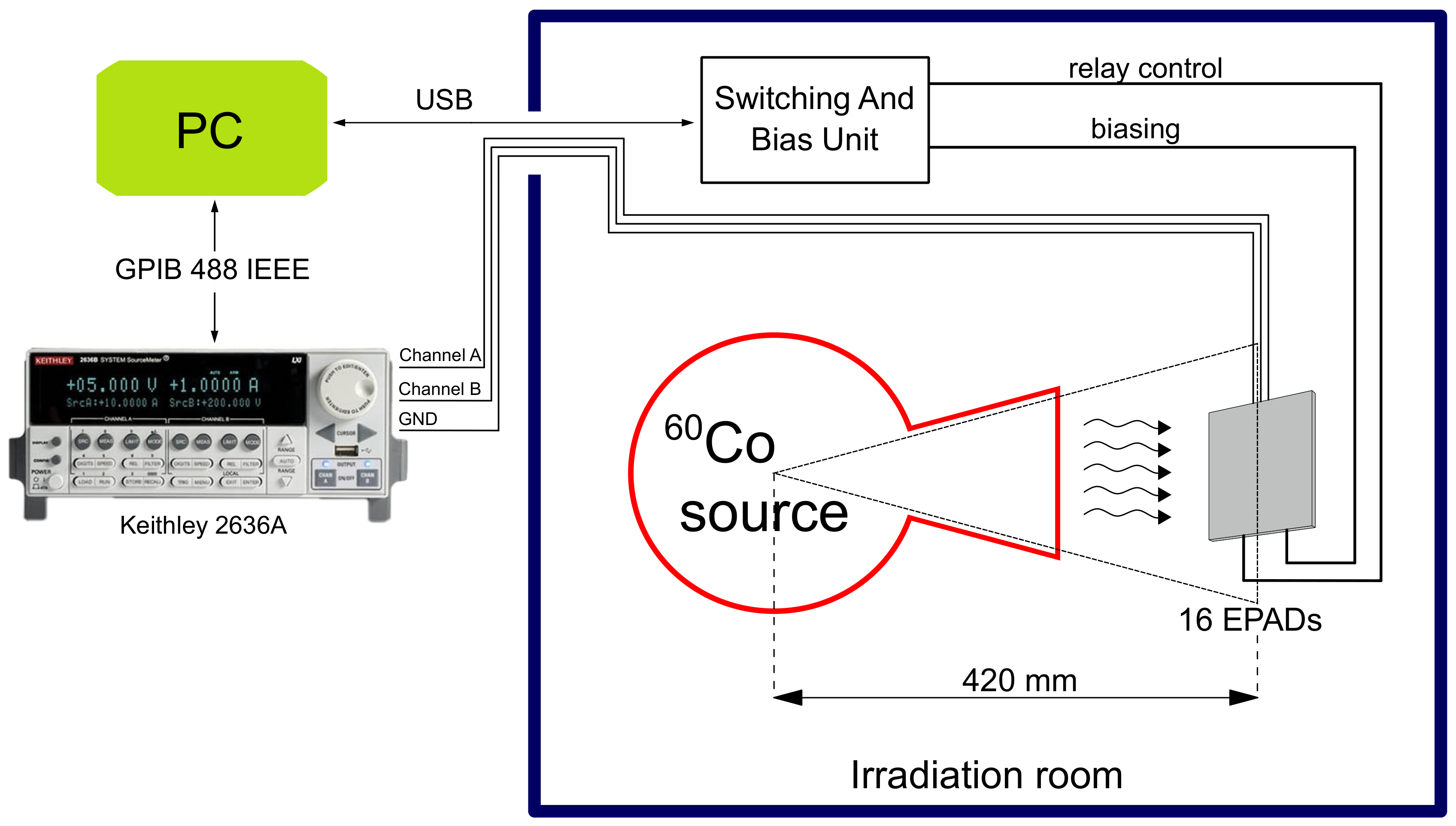
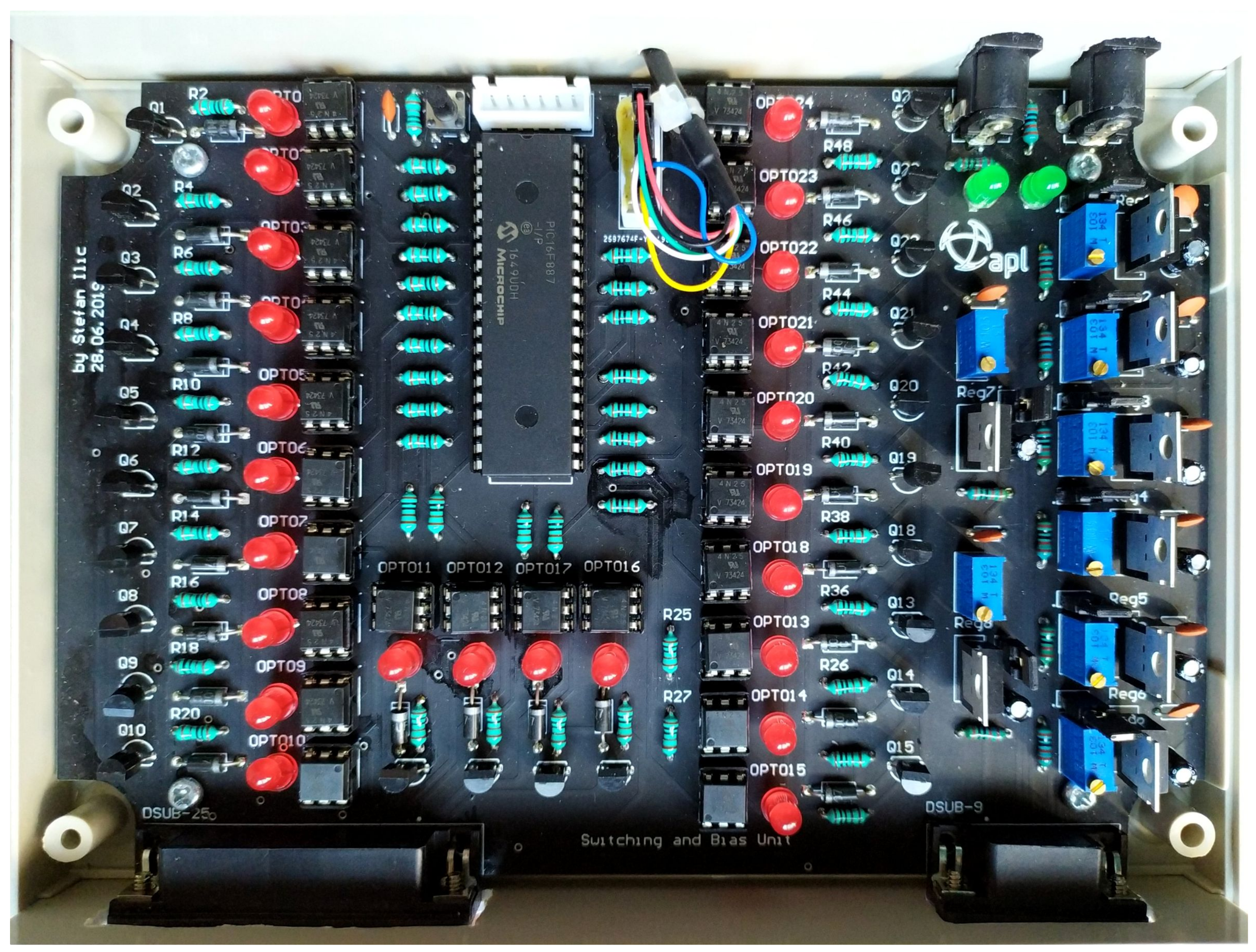
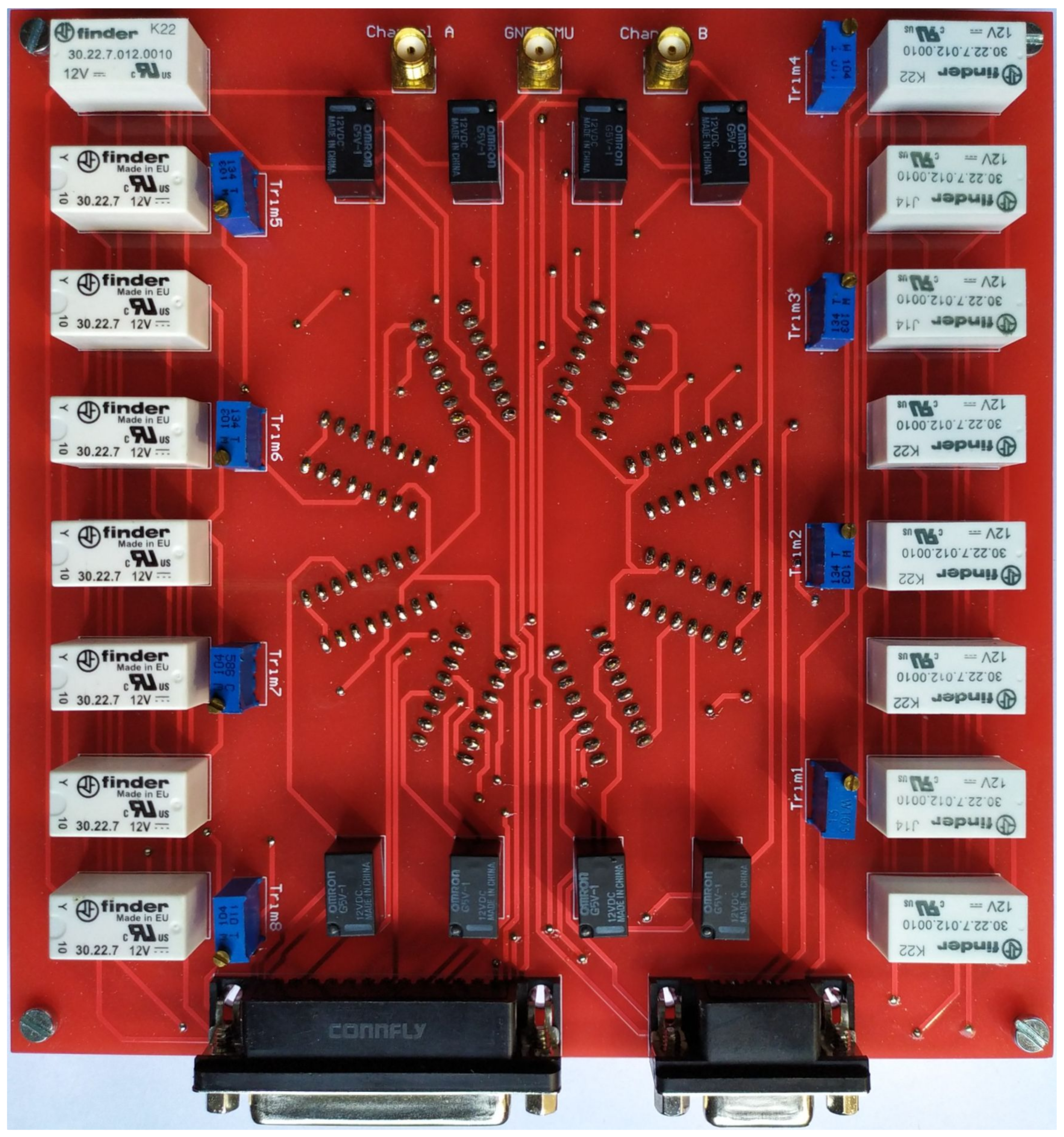
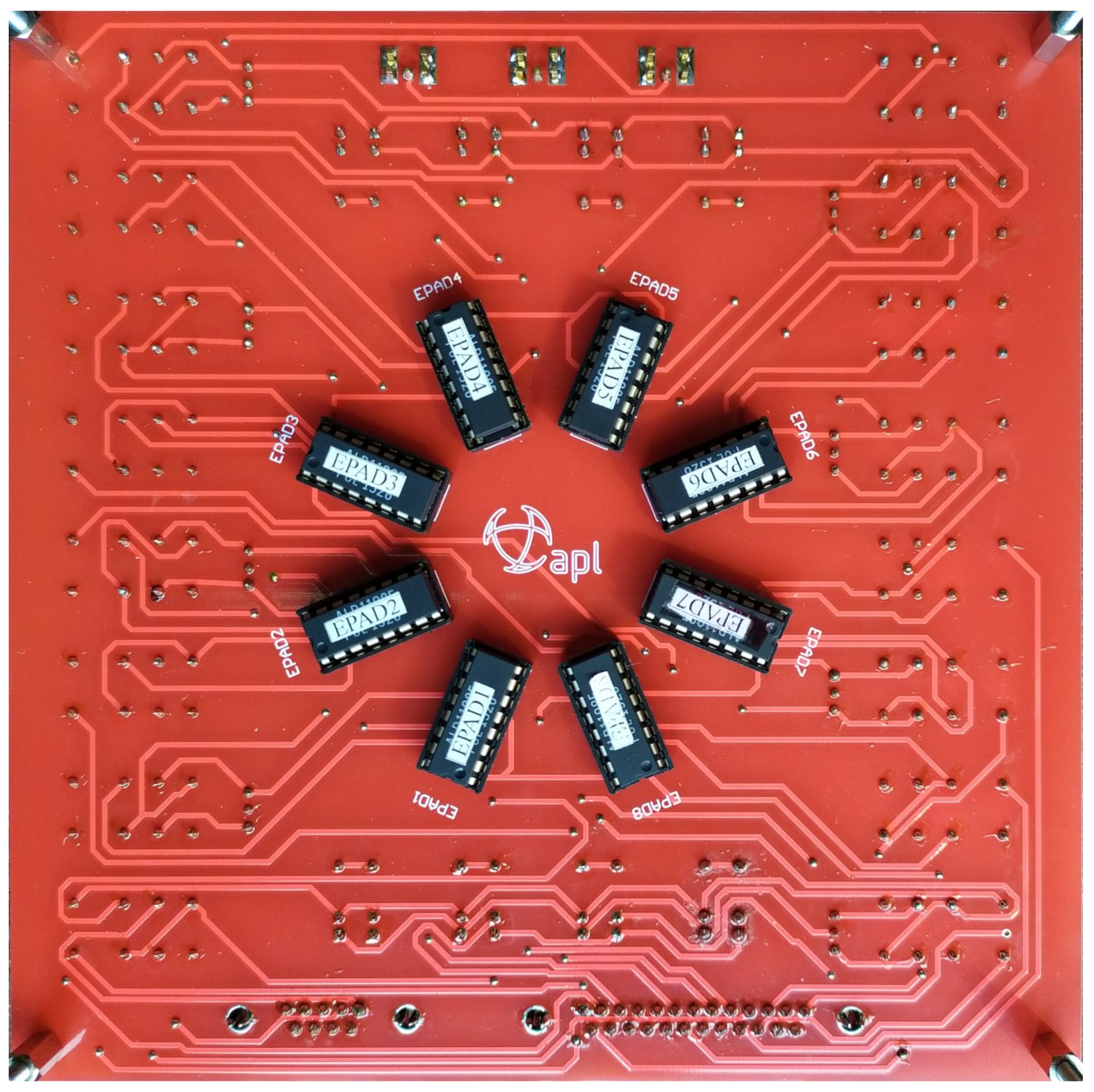
2.3. Automated System for Measurements
2.4. Experimental Setup
3. Results
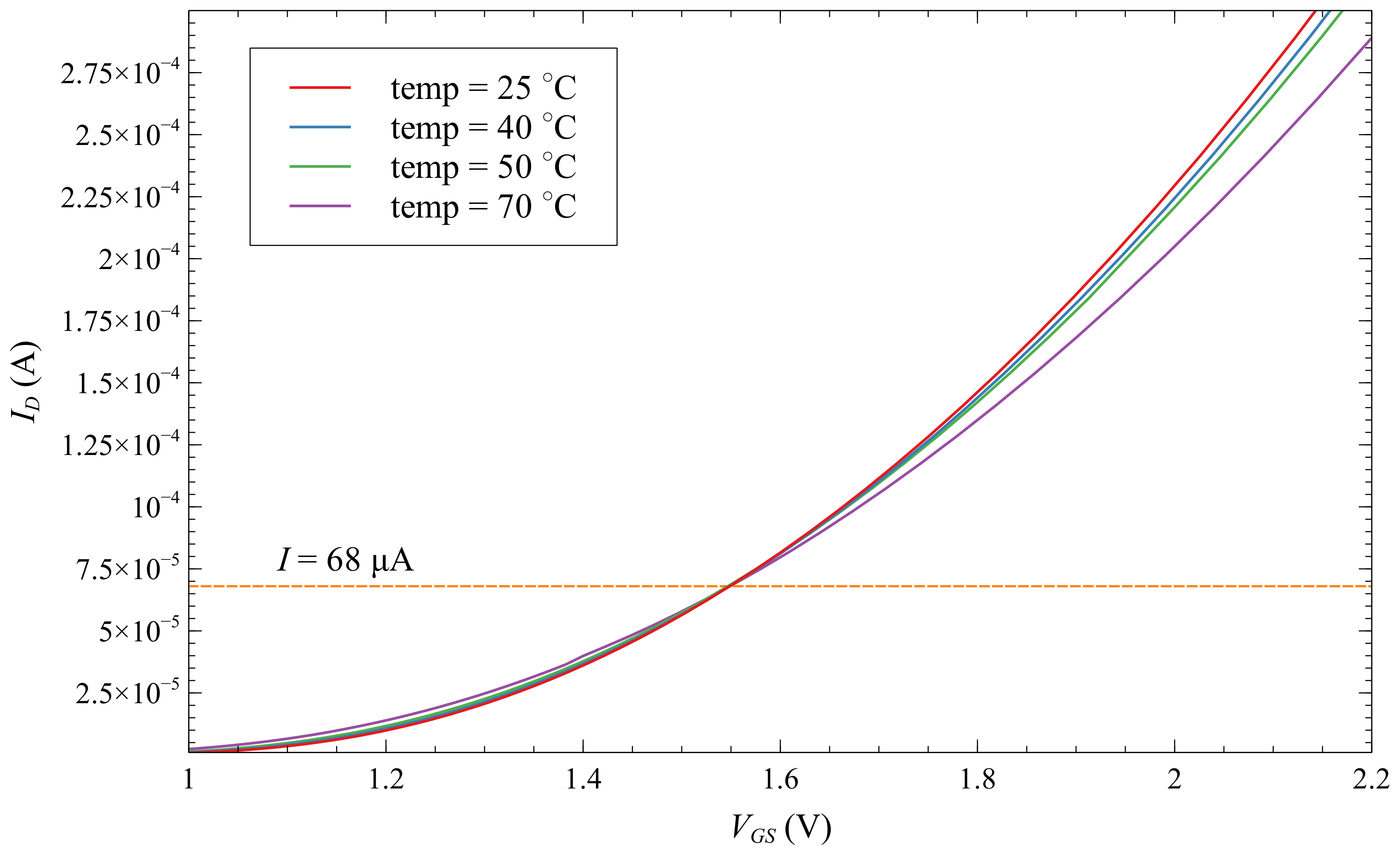
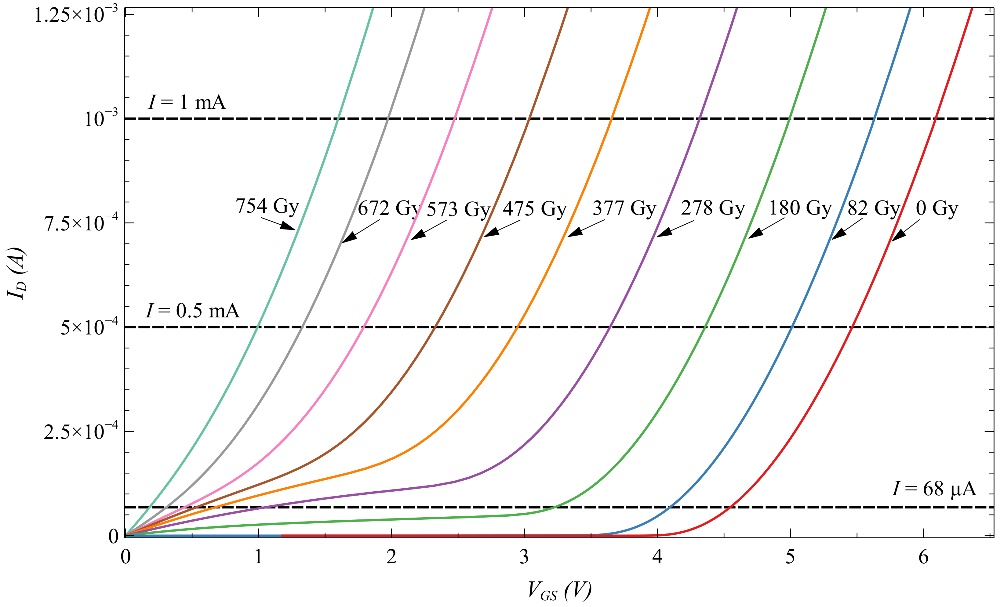
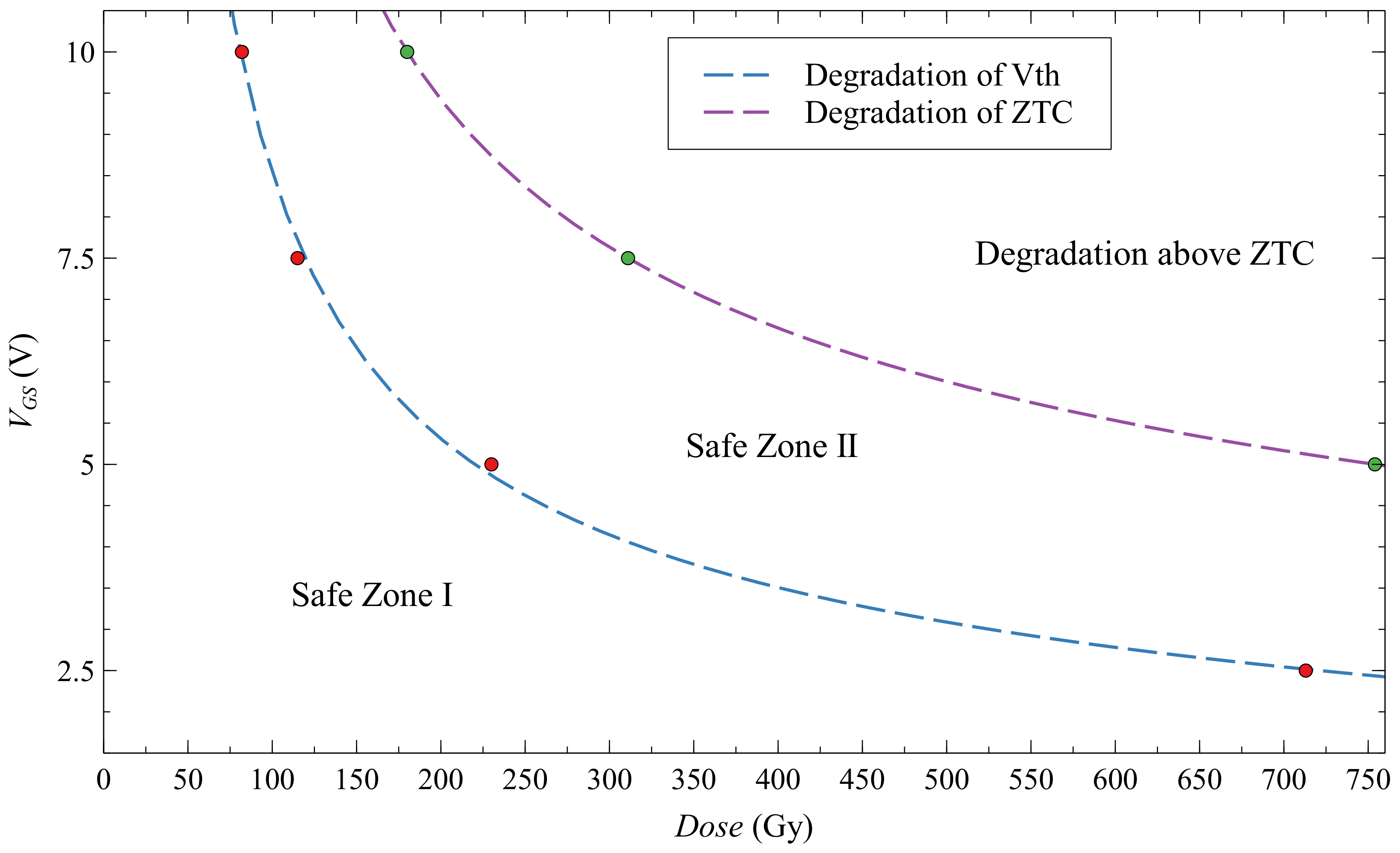
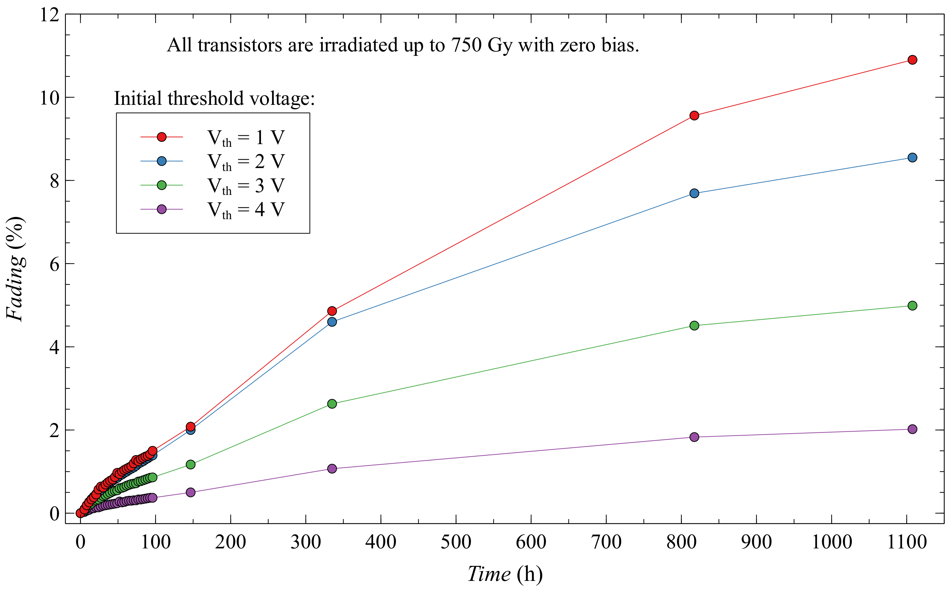
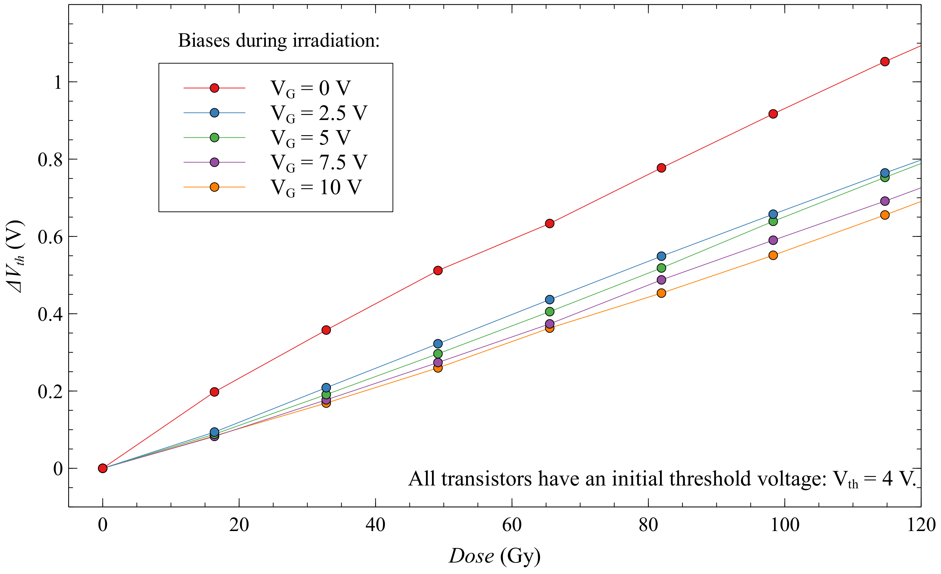
3.1. Static Bias
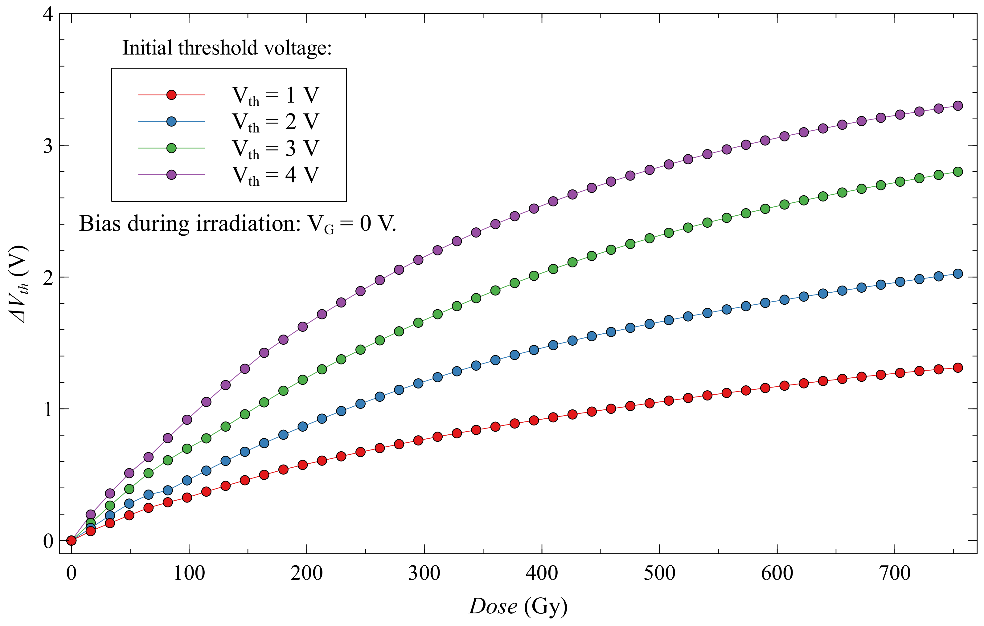
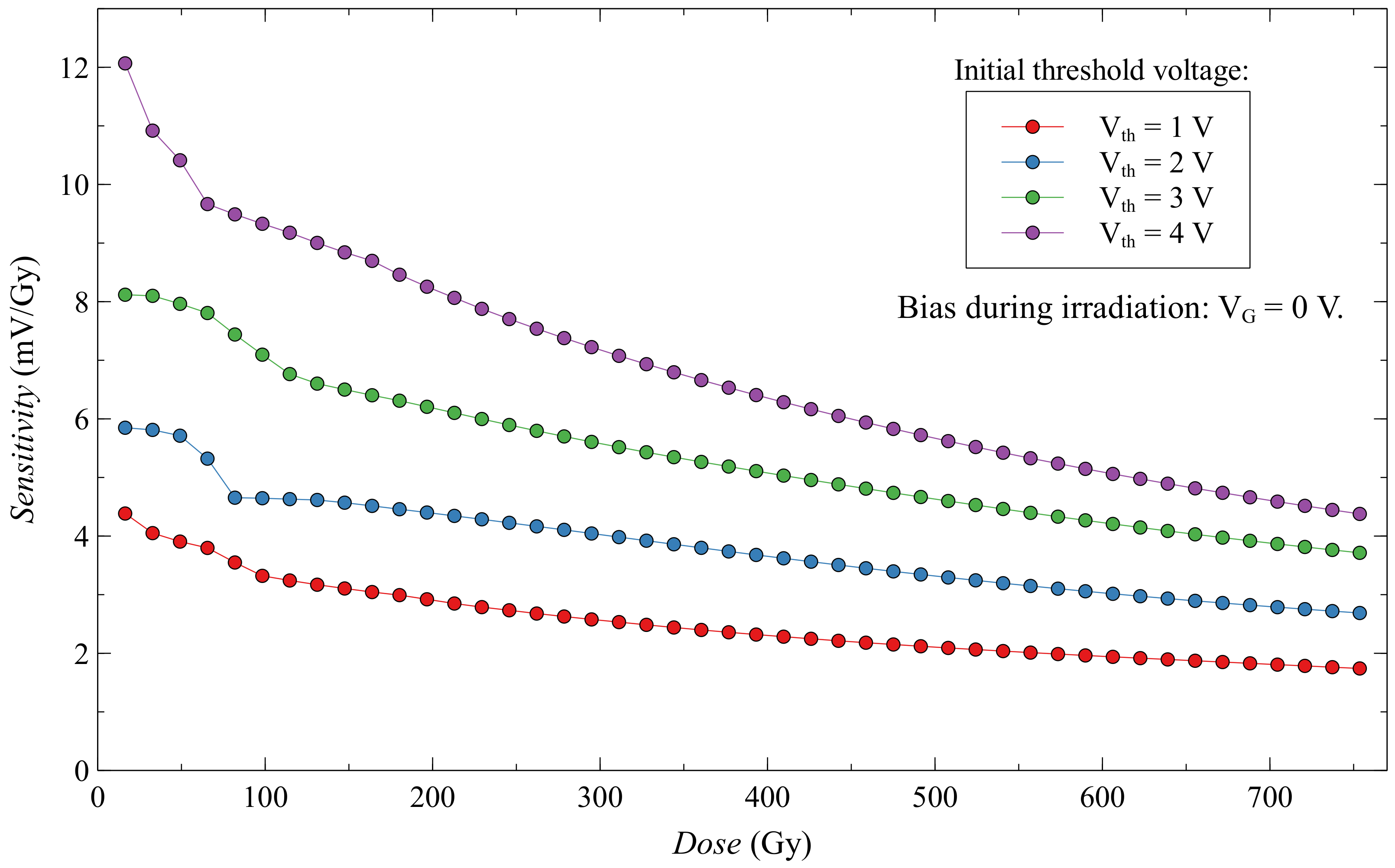
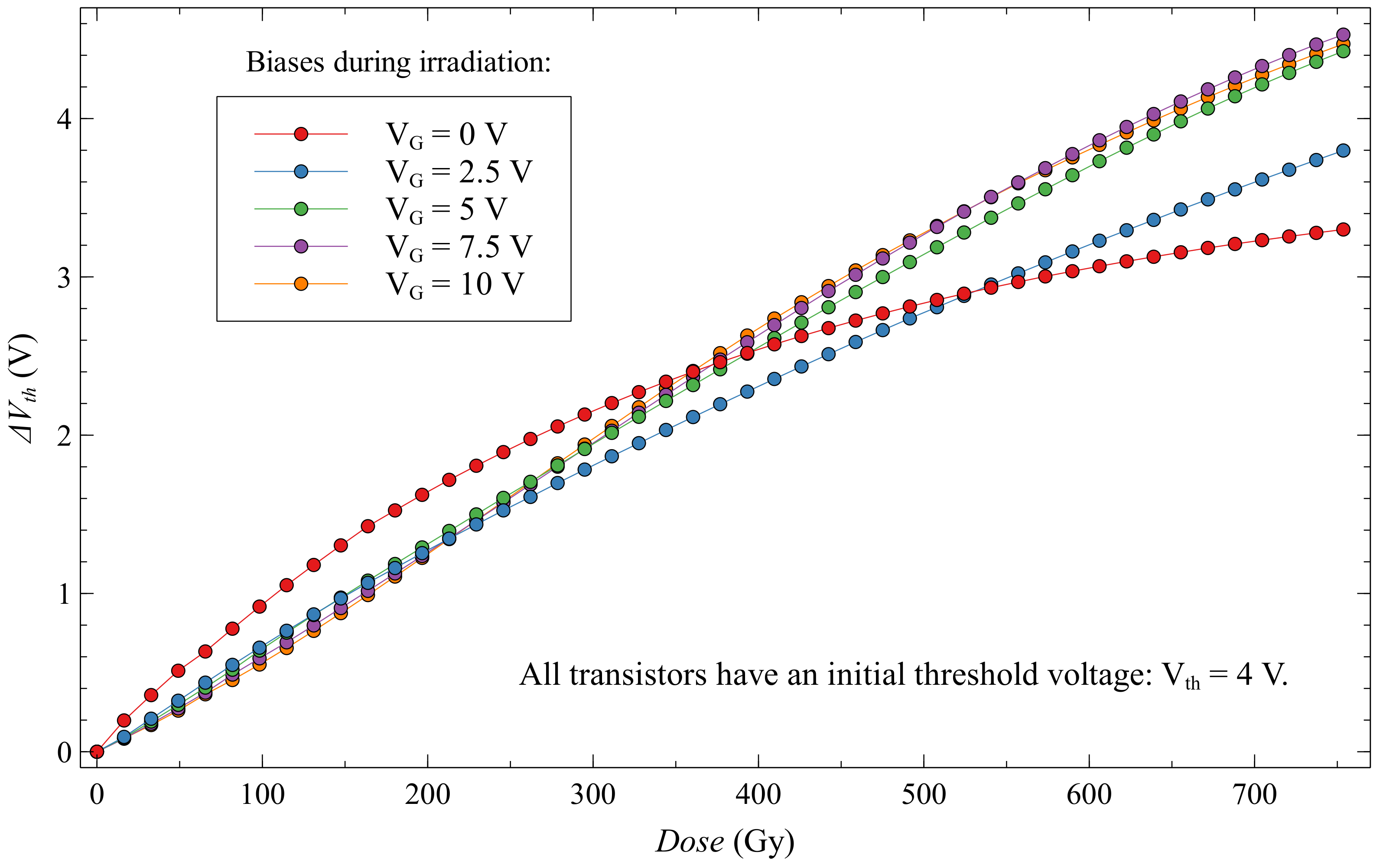
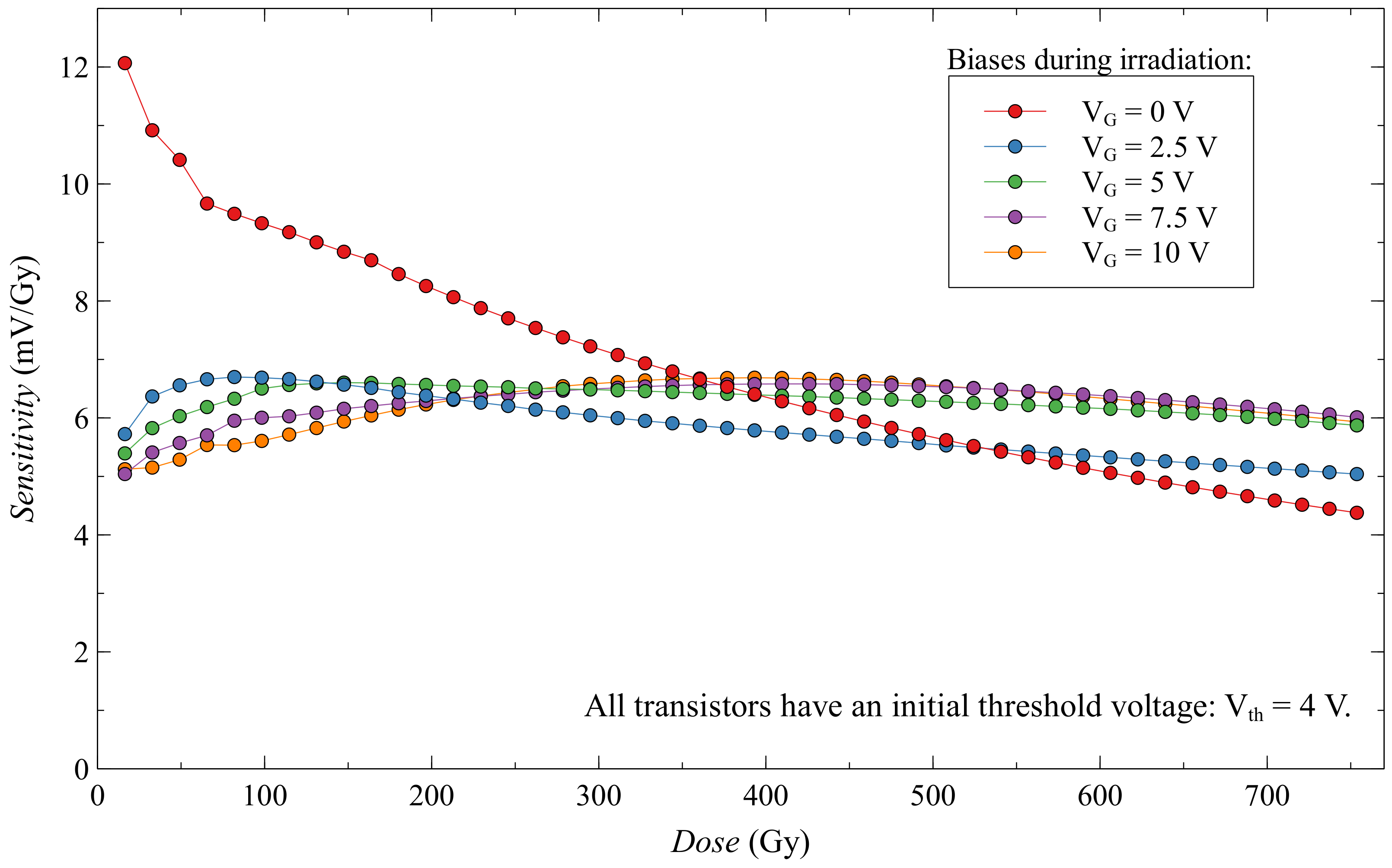
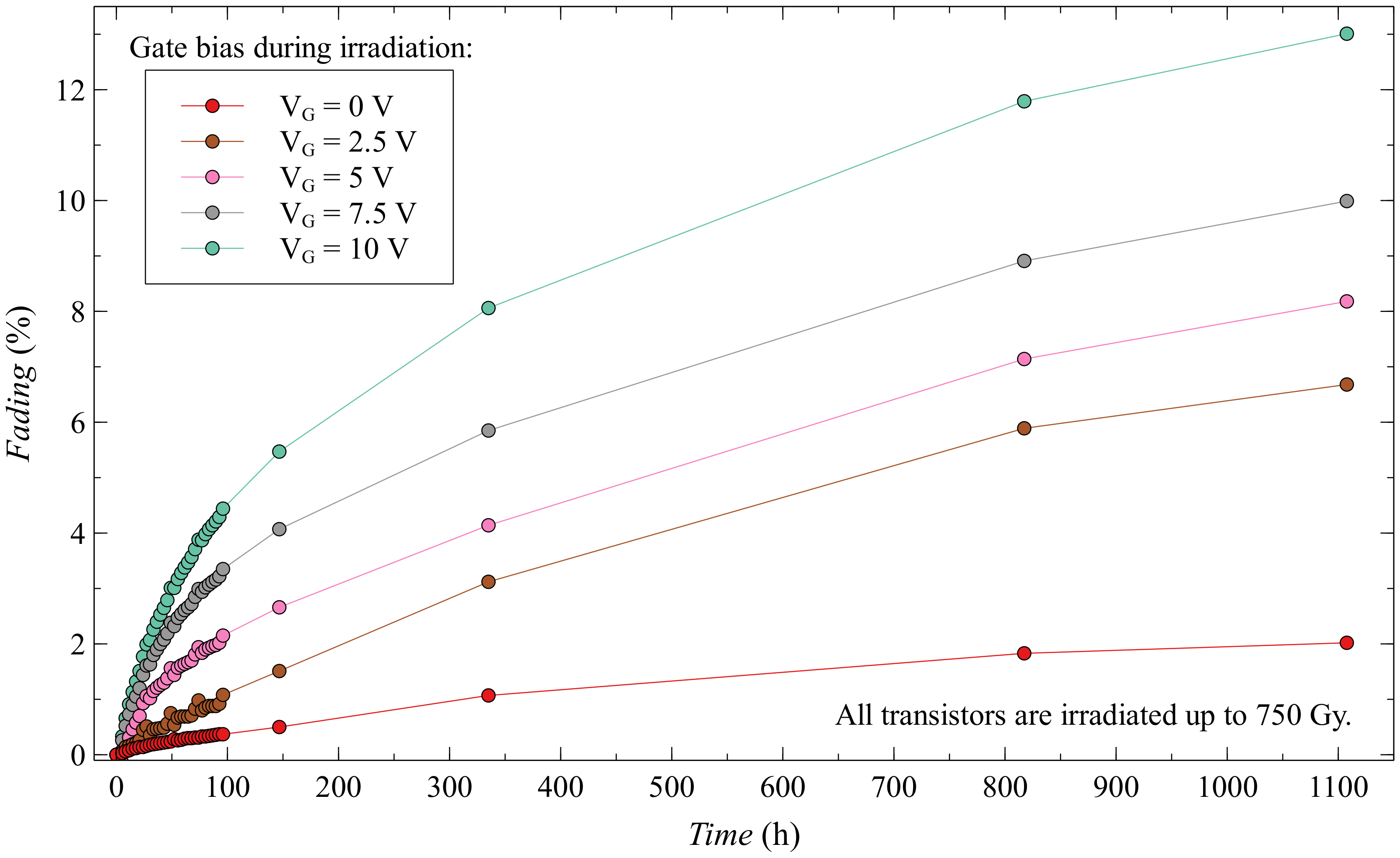
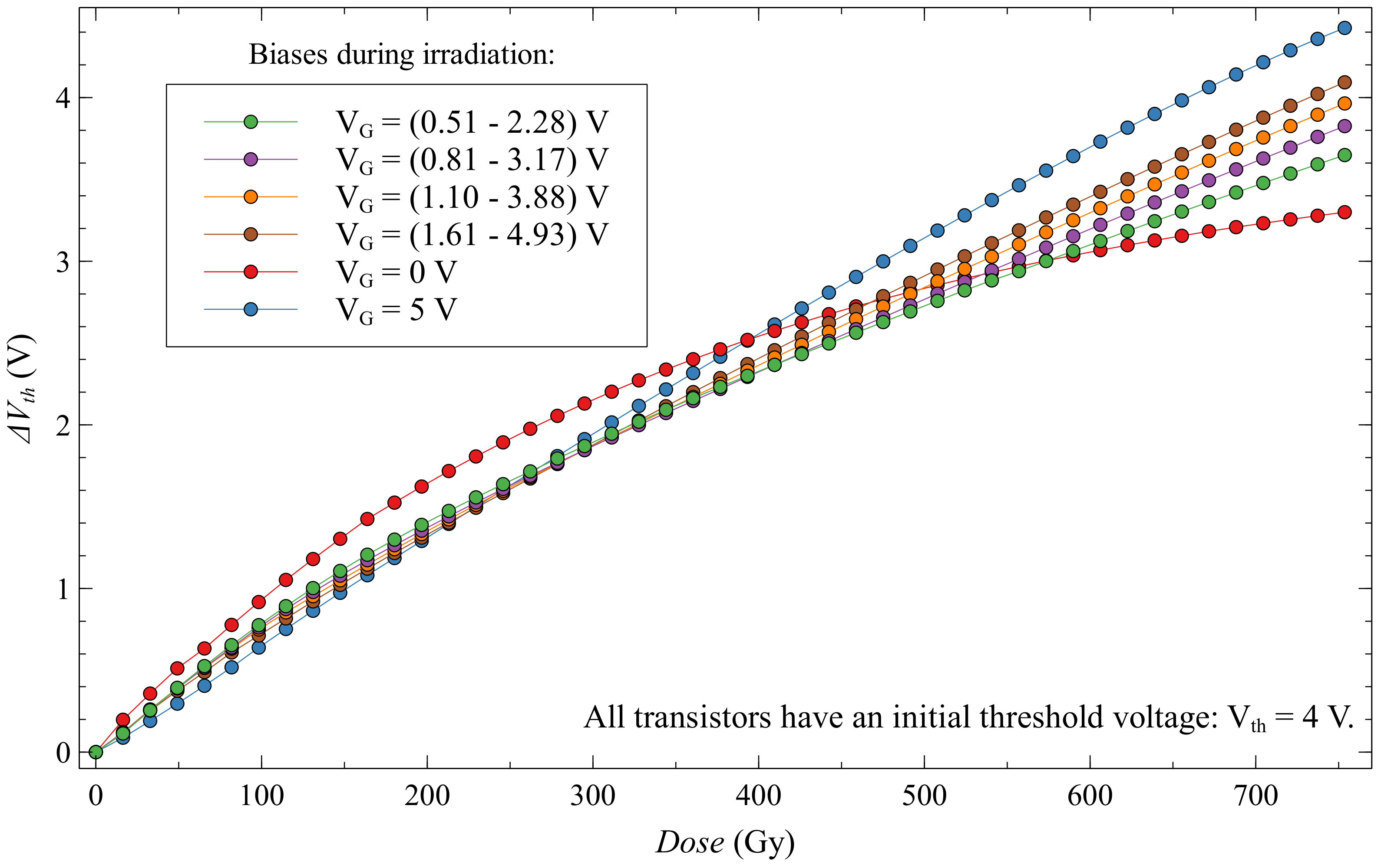
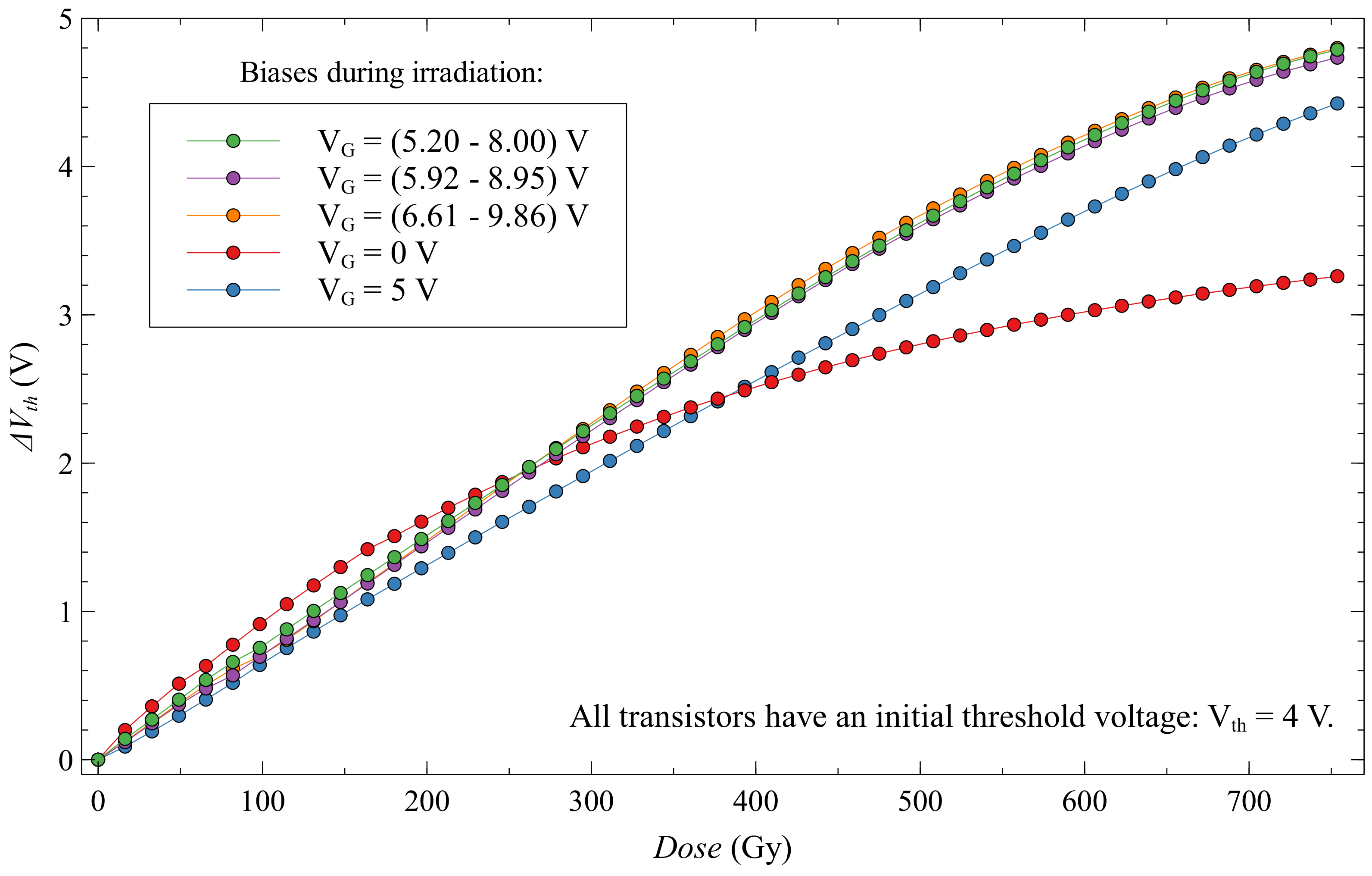
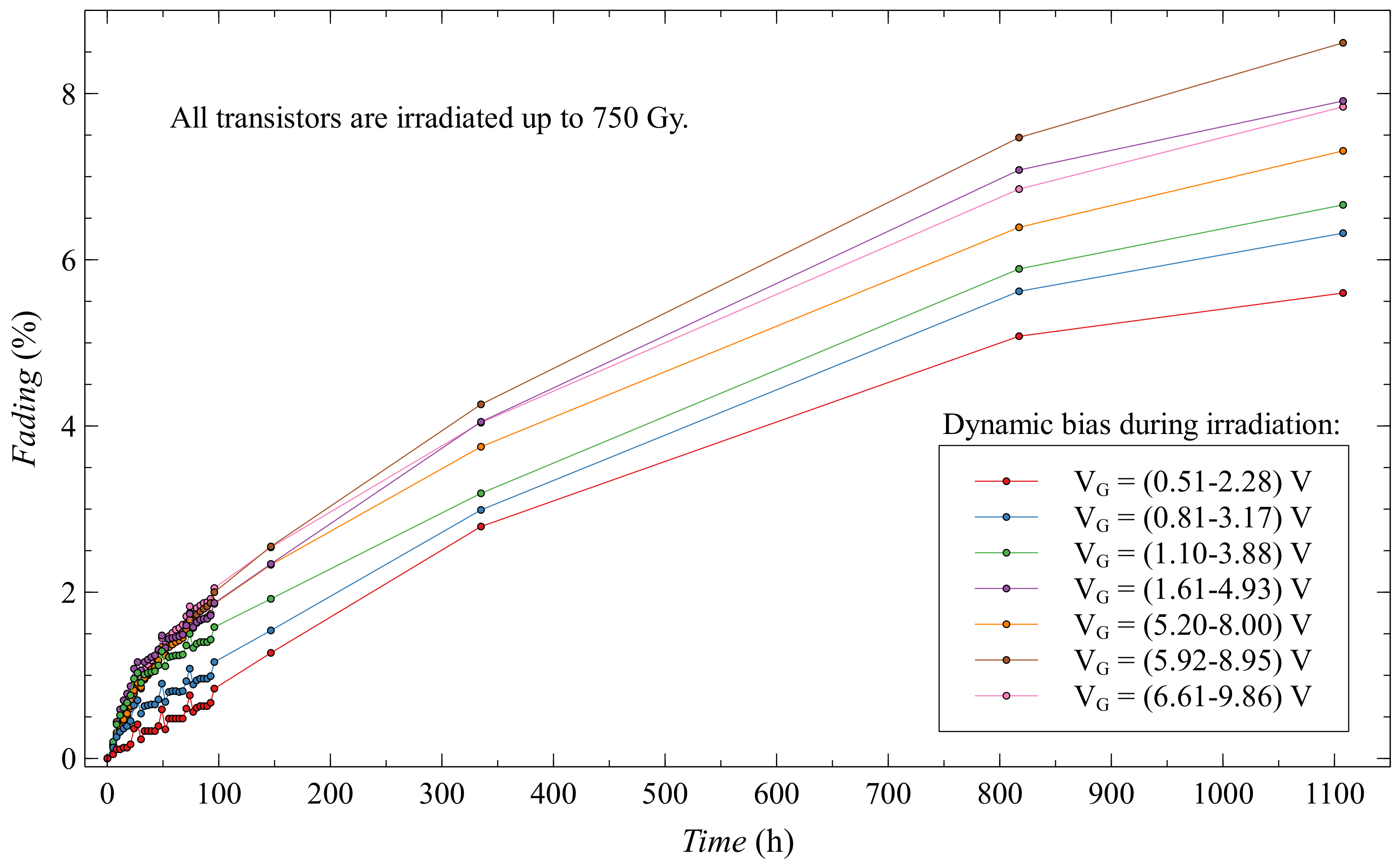
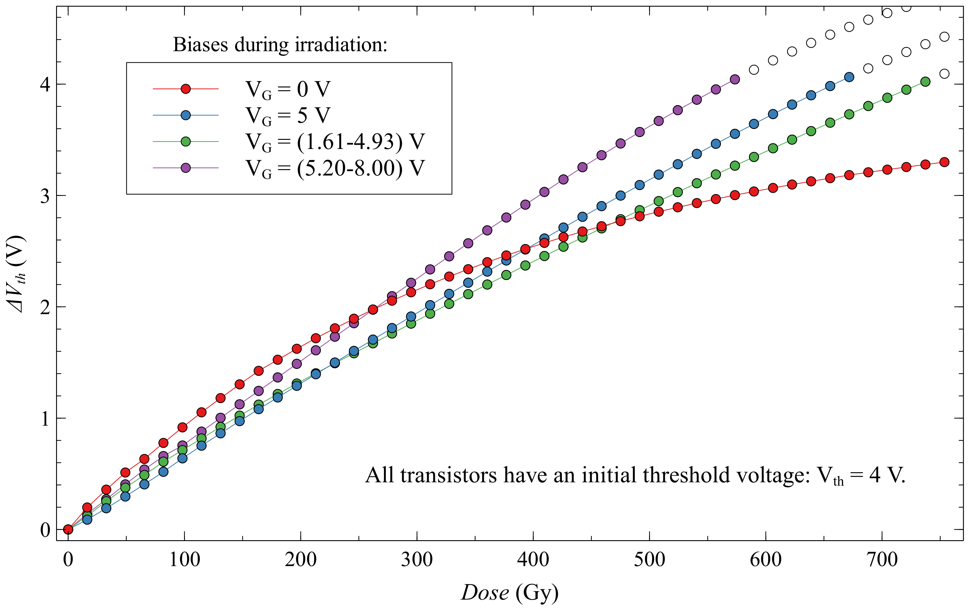
3.2. Dynamic Bias
4. Discussion
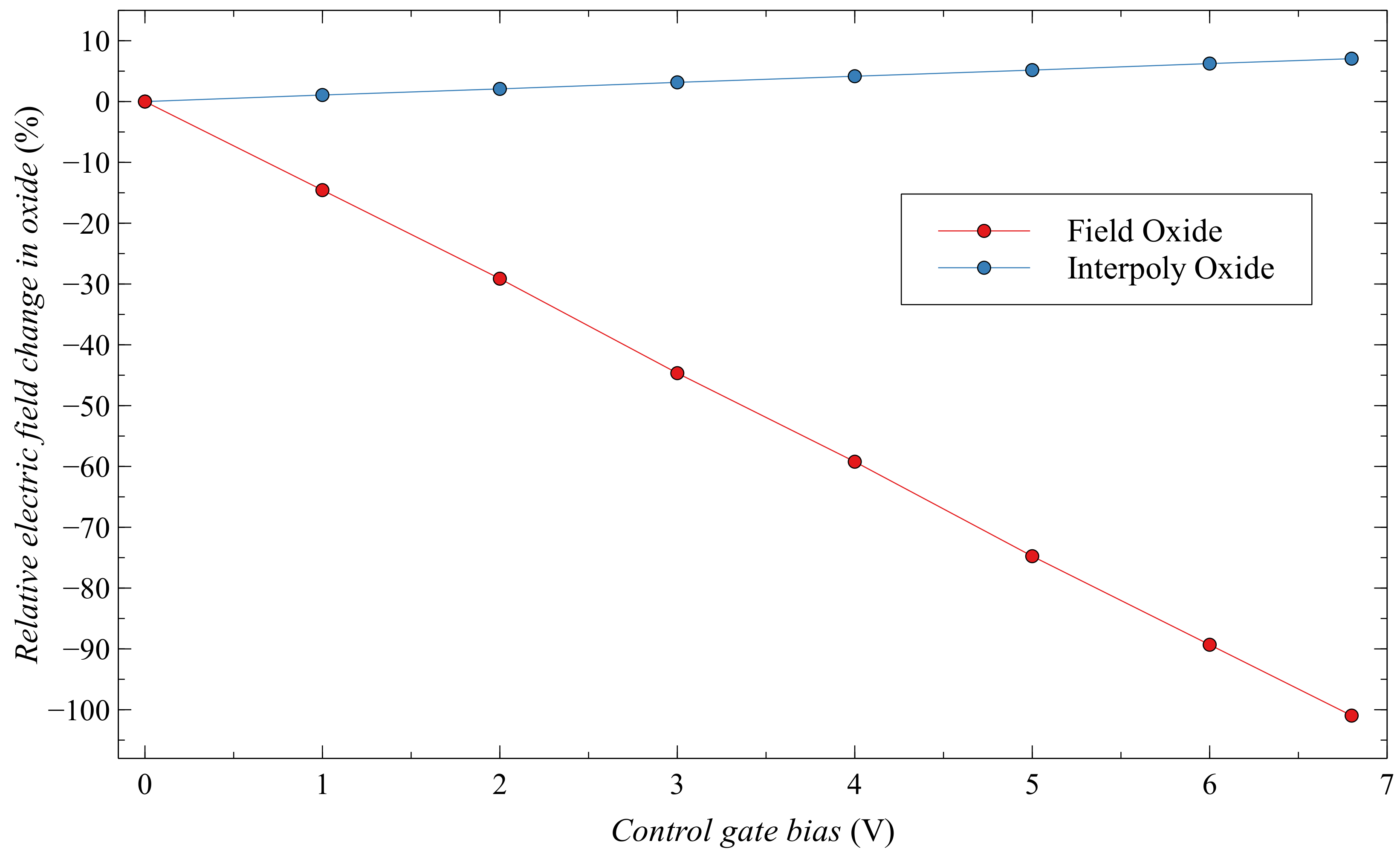
4.1. Energy Band Diagram
4.2. Epad Future Applications
5. Conclusions
Author Contributions
Funding
Acknowledgments
Conflicts of Interest
Abbreviations
| EPAD | Electrically Programmable Analog Device |
| ZTC | Zero Temperature Coefficient |
| SMU | Source Measure Unit |
| GPIB | General-Purpose Interface Bus |
| ICSP | In-Circuit Serial Programming |
| FTDI | Future Technology Devices International |
| PMMA | Poly(Methyl Methacrylate) |
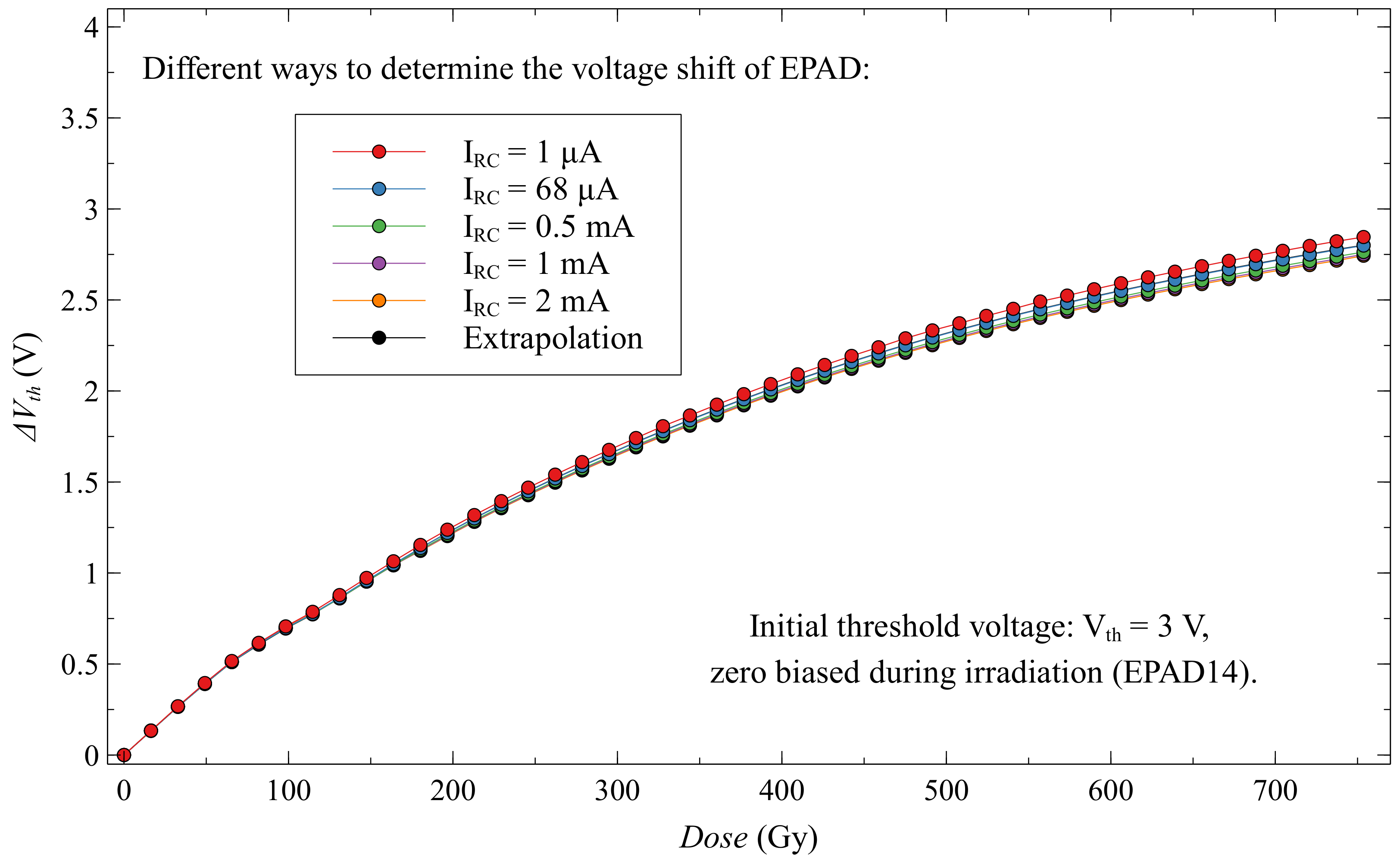
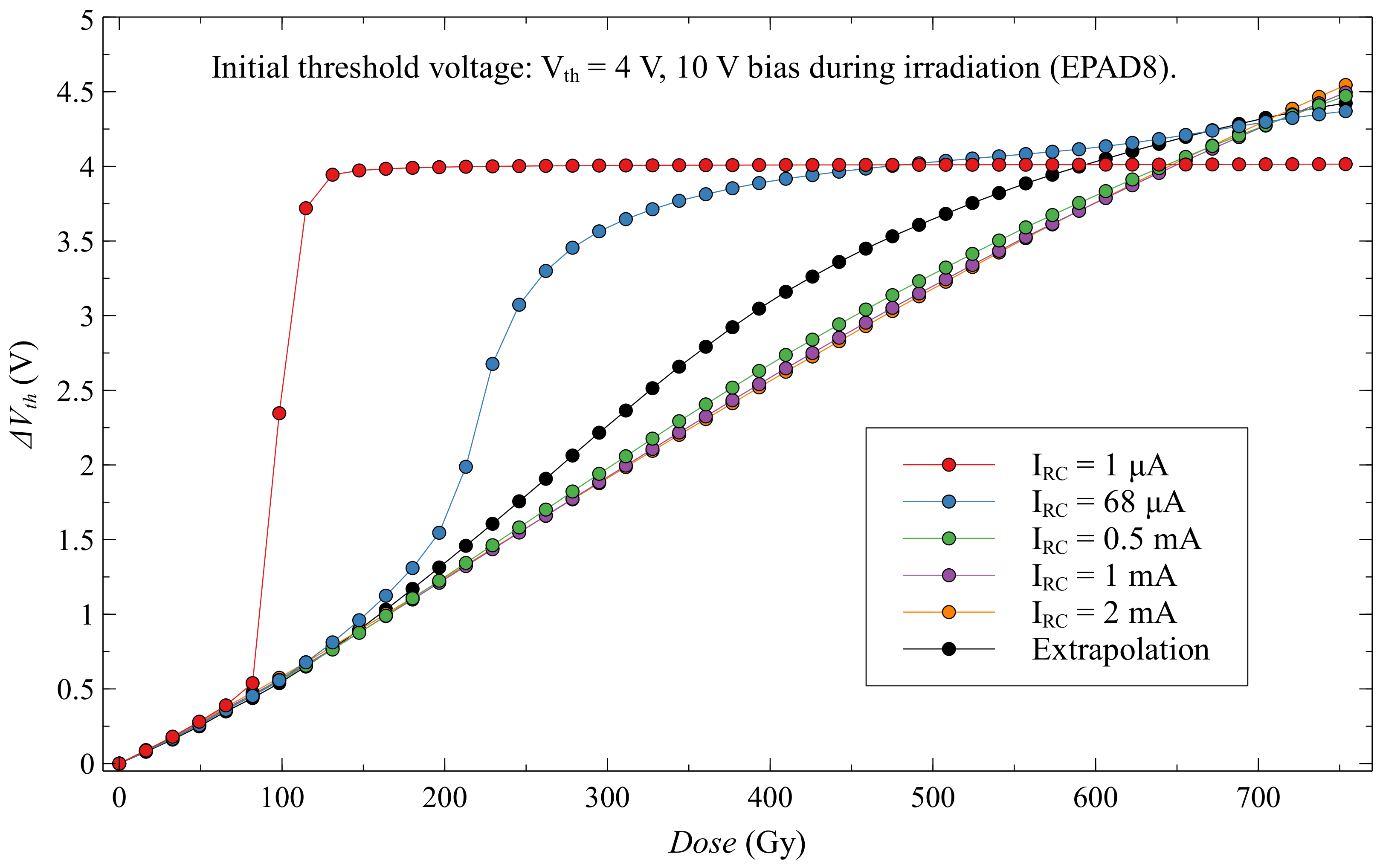
Appendix A. Reader-Circuit Currents


Appendix B. Photos of the Automated Measurement System


References
- Shapiro, S.L.; Dunwoodie, W.M.; Arens, J.; Jernigan, J.G.; Gaalema, S. Silicon PIN diode array hybrids for charged particle detection. Nucl. Instrum. Methods Phys. Res. 1988, A275, 580–586. [Google Scholar] [CrossRef]
- Anđelković, M.S.; Ristić, G.S. Feasibility study of a current mode gamma radiation dosimeter based on a commercial pin photodiode and a custom made auto-ranging electrometer. Nucl. Technol. Radiat. Prot. 2013, 28, 73–83. [Google Scholar] [CrossRef]
- Magalhães, C.; Sobrinho, M.; Souza, D.; Filho, J.A.; da Silva, E.; Santos, L. A novel dosimetry system for computed tomography using phototransistor. Radiat. Meas. 2012, 47, 30–33. [Google Scholar] [CrossRef][Green Version]
- Andjelković, M.S.; Ristić, G.S. Current mode response of phototransistors to gamma radiation. Radiat. Meas. 2015, 75, 29–38. [Google Scholar] [CrossRef]
- Román-Raya, J.; Ruiz-García, I.; Escobedo, P.; Palma, A.J.; Guirado, D.; Carvajal, M.A. Light-Dependent Resistors as Dosimetric Sensors in Radiotherapy. Sensors 2020, 20, 1568. [Google Scholar] [CrossRef] [PubMed]
- Jaksic, A.; Kimoto, Y.; Mohammadzadeh, A.; Mathewson, A. Dose rate dependence of RADFET irradiation and post-irradiation responses. In Proceedings of the 2004 24th International Conference on Microelectronics (IEEE Cat. No.04TH8716), Niš, Serbia, 16–19 May 2004; Volume 2, pp. 661–664. [Google Scholar]
- Haran, A.; Jaksic, A.; Refaeli, N.; Eliyahu, A.; David, D.; Barak, J. Temperature effects and long term fading of implanted and unimplanted gate oxide RADFETs. IEEE Trans. Nucl. Sci. 2004, 51, 2917–2921. [Google Scholar] [CrossRef]
- Kaya, S.; Jaksic, A.; Duane, R.; Vasovic, N.; Yilmaz, E. FET-based radiation sensors with Er2O3 gate dielectric. Nucl. Instrum. Methods Phys. Res. Sect. Beam Interact. Mater. At. 2018, 430, 36–41. [Google Scholar] [CrossRef]
- Danković, D.; Manić, I.; Davidović, V.; Djorić-Veljković, S.; Golubović, S.; Stojadinović, N. Negative bias temperature instability in n-channel power VDMOSFETs. Microelectron. Reliab. 2008, 48, 1313–1317. [Google Scholar] [CrossRef]
- Davidović, V.; Danković, D.; Ilić, A.; Manić, I.; Golubović, S.; Djorić-Veljković, S.; Prijić, Z.; Stojadinović, N. NBTI and Irradiation Effects in P-Channel Power VDMOS Transistors. IEEE Trans. Nucl. Sci. 2016, 63, 1268–1275. [Google Scholar] [CrossRef]
- Holmes-Siedle, A. The space-charge dosimeter: General principles of a new method of radiation detection. Nucl. Instrum. Methods 1974, 121, 169–179. [Google Scholar] [CrossRef]
- Hughes, R.C.; Dawes, W.R.; Meyer, W.J.; Yoon, S.W. Dual dielectric silicon metal-oxide-semiconductor field-effect transistors as radiation sensors. J. Appl. Phys. 1989, 65, 1972–1976. [Google Scholar] [CrossRef]
- Kassabov, J.; Nedev, N.; Smirnov, N. Radiation dosimeter based on floating gate MOS transistor. Radiat. Eff. Defects Solids 1991, 116, 155–158. [Google Scholar] [CrossRef]
- Snyder, E.S.; McWhorter, P.J.; Dellin, T.A.; Sweetman, J.D. Radiation response of floating gate EEPROM memory cells. IEEE Trans. Nucl. Sci. 1989, 36, 2131–2139. [Google Scholar] [CrossRef]
- Kahilainen, J. The Direct Ion Storage Dosemeter. Radiat. Prot. Dosim. 1996, 66, 459–462. [Google Scholar] [CrossRef]
- Mathur, V. Ion storage dosimetry. Nucl. Instrum. Methods Phys. Res. Sect. Beam Interact. Mater. At. 2001, 184, 190–206. [Google Scholar] [CrossRef]
- Pavan, P.; Larcher, L.; Marmiroli, A. Floating Gate Devices: Operation and Compact Modeling; Springer: New York, NY, USA, 2004. [Google Scholar]
- Ristic, G.S.; Andjelkovic, M.; Jaksic, A.B. The behavior of fixed and switching oxide traps of RADFETs during irradiation up to high absorbed doses. Appl. Radiat. Isot. 2015, 102, 29–34. [Google Scholar] [CrossRef] [PubMed]
- Savić, Z.; Radjenović, B.; Pejović, M.; Stojadinović, N. The contribution of border traps to the threshold voltage shift in pMOS dosimetric transistors. IEEE Trans. Nucl. Sci. 1995, 42, 1445–1454. [Google Scholar] [CrossRef]
- Ristić, G.; Golubović, S.; Pejović, M. P-channel metal–oxide–semiconductor dosimeter fading dependencies on gate bias and oxide thickness. Appl. Phys. Lett. 1995, 66, 88–89. [Google Scholar] [CrossRef]
- Waser, R. Nanoelectronics and Information Technology, 3rd ed.; Wiley-VCH: Weinheim, Germany, 2012. [Google Scholar]
- ALD. QUAD/DUAL Electrically Programmable Analog Device. 2012. Available online: https://www.aldinc.com/pdf/ALD1110E.pdf2012 (accessed on 7 June 2020).
- Available online: https://www.aldinc.com/pdf/AN1108.pdf (accessed on 7 June 2020).
- Jevtic, A.; Ilic, S.; Davidovic, V.; Prijic, Z.; Prijic, A. Characterization of electrically programmable floating gate MOS transistor. In Proceedings of the 62nd Annual Meeting of ETRAN Society, Palić, Serbia, 11–14 June 2018; pp. 304–307. [Google Scholar]
- Edgecock, R.; Matheson, J.; Weber, M.; Villani, E.G.; Bose, R.; Khan, A.; Smith, D.; Adil-Smith, I.; Gabrielli, A. Evaluation of commercial programmable floating gate devices as radiation dosimeters. J. Instrum. 2009, 4, P02002. [Google Scholar] [CrossRef]
- Bose, R. The development of an in-vivo dosimeter for the application in radiotherapy. Ph.D. Thesis, Brunel University, London, UK, 2012. [Google Scholar]
- Ilic, S.; Jevtic, A.; Stankovic, S.; Davidovic, V. Feasibility of Applying an Electrically Programmable Floating-Gate MOS Transistor in Radiation Dosimetry. In Proceedings of the IEEE 31st International Conference On Microelectronics. IEEE Serbia and Montenegro Section—ED/SSC Chapter, Niš, Serbia, 16–18 September 2019; pp. 67–70. [Google Scholar]
- Jevtic, A.; Ilic, S.; Davidovic, V. EPADs decapsulation and analysis. In Proceedings of the 11th Student Project Conference “IEEESTEC 2018”, Niš, Serbia, 29 November 2018; pp. 329–333. [Google Scholar]
- Tarr, N.G.; Mackay, G.F.; Shortt, K.; Thomson, I. A floating gate MOSFET dosimeter requiring no external bias supply. In Proceedings of the RADECS 97, Fourth European Conference on Radiation and Its Effects on Components and Systems (Cat. No.97TH8294), Cannes, France, 15–19 September 1997; pp. 277–281. [Google Scholar] [CrossRef]
- Garry Tarr, N. Method of Monitoring Radiation Using a Floating Gate Field Effect Transistor Dosimeter, and Dosimeter for Use Therein. US Patent 6,172,368 B1, 9 January 2001. [Google Scholar]
- Ristic, G.; Golubovic, S.; Pejovic, M. Sensitivity and fading of pMOS dosimeters with thick gate oxide. Sens. Actuators A Phys. 1996, 51, 153–158. [Google Scholar] [CrossRef]
- Vasović, N.D.; Ristić, G.S. A new microcontroller-based RADFET dosimeter reader. Radiat. Meas. 2012, 47, 272–276. [Google Scholar] [CrossRef]
- Ristic, G.S. Influence of ionizing radiation and hot carrier injection on metal-oxide-semiconductor transistors. J. Phys. D Appl. Phys. 2008, 41, 023001. [Google Scholar] [CrossRef]
- Southwick, R.G.; Knowlton, W.B. Stacked dual-oxide MOS energy band diagram visual representation program (IRW student paper). IEEE Trans. Device Mater. Reliab. 2006, 6, 136–145. [Google Scholar] [CrossRef]
- Southwick, R.G.; Sup, A.; Jain, A.; Knowlton, W.B. An Interactive Simulation Tool for Complex Multilayer Dielectric Devices. IEEE Trans. Device Mater. Reliab. 2011, 11, 236–243. [Google Scholar] [CrossRef]
- Brucoli, M.; Danzeca, S.; Brugger, M.; Masi, A.; Pineda, A.; Cesari, J.; Dusseau, L.; Wrobel, F. Floating Gate Dosimeter Suitability for Accelerator-Like Environments. IEEE Trans. Nucl. Sci. 2017, 64, 2054–2060. [Google Scholar] [CrossRef]
- Ferraro, R.; Danzeca, S.; Brucoli, M.; Masi, A.; Brugger, M.; Dilillo, L. Design of a radiation tolerant system for total ionizing dose monitoring using floating gate and RadFET dosimeters. J. Instrum. 2017, 12, C04007. [Google Scholar] [CrossRef]
- Brucoli, M.; Cesari, J.; Danzeca, S.; Brugger, M.; Masi, A.; Pineda, A.; Dusseau, L.; Wrobel, F. Investigation on Passive and Autonomous Mode Operation of Floating Gate Dosimeters. IEEE Trans. Nucl. Sci. 2019, 66, 1620–1627. [Google Scholar] [CrossRef]


| Name | Bias During Irradiation | Initial |
|---|---|---|
| EPAD2 | 2.5 V | 4 V |
| EPAD4 | 5 V | 4 V |
| EPAD6 | 7.5 V | 4 V |
| EPAD8 | 10 V | 4 V |
| EPAD10 | 0 V | 1 V |
| EPAD12 | 0 V | 2 V |
| EPAD14 | 0 V | 3 V |
| EPAD16 | 0 V | 4 V |
| Name | Biasing | ||
|---|---|---|---|
| EPAD1 | 6 V | 1 k | (0.51–2.28) V |
| EPAD3 | 6 V | 2.5 k | (0.81–3.17) V |
| EPAD5 | 6 V | 6 k | (1.10–3.88) V |
| EPAD7 | 6 V | 50 k | (1.61–4.93) V |
| EPAD9 | 12 V | 3 k | (5.20–8.00) V |
| EPAD11 | 12 V | 6 k | (5.92–8.95) V |
| EPAD13 | 12 V | 15 k | (6.61–9.86) V |
| EPAD15 | 12 V | 100 k | (7.40–10.9) V |
© 2020 by the authors. Licensee MDPI, Basel, Switzerland. This article is an open access article distributed under the terms and conditions of the Creative Commons Attribution (CC BY) license (http://creativecommons.org/licenses/by/4.0/).
Share and Cite
Ilić, S.; Jevtić, A.; Stanković, S.; Ristić, G. Floating-Gate MOS Transistor with Dynamic Biasing as a Radiation Sensor. Sensors 2020, 20, 3329. https://doi.org/10.3390/s20113329
Ilić S, Jevtić A, Stanković S, Ristić G. Floating-Gate MOS Transistor with Dynamic Biasing as a Radiation Sensor. Sensors. 2020; 20(11):3329. https://doi.org/10.3390/s20113329
Chicago/Turabian StyleIlić, Stefan, Aleksandar Jevtić, Srboljub Stanković, and Goran Ristić. 2020. "Floating-Gate MOS Transistor with Dynamic Biasing as a Radiation Sensor" Sensors 20, no. 11: 3329. https://doi.org/10.3390/s20113329
APA StyleIlić, S., Jevtić, A., Stanković, S., & Ristić, G. (2020). Floating-Gate MOS Transistor with Dynamic Biasing as a Radiation Sensor. Sensors, 20(11), 3329. https://doi.org/10.3390/s20113329