A 1-nS 1-V Sub-1-µW Linear CMOS OTA with Rail-to-Rail Input for Hz-Band Sensory Interfaces

 ,
,  , , and
Abstract
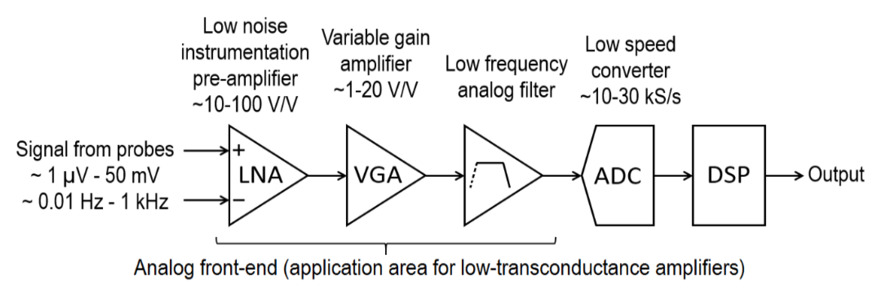
1. Introduction
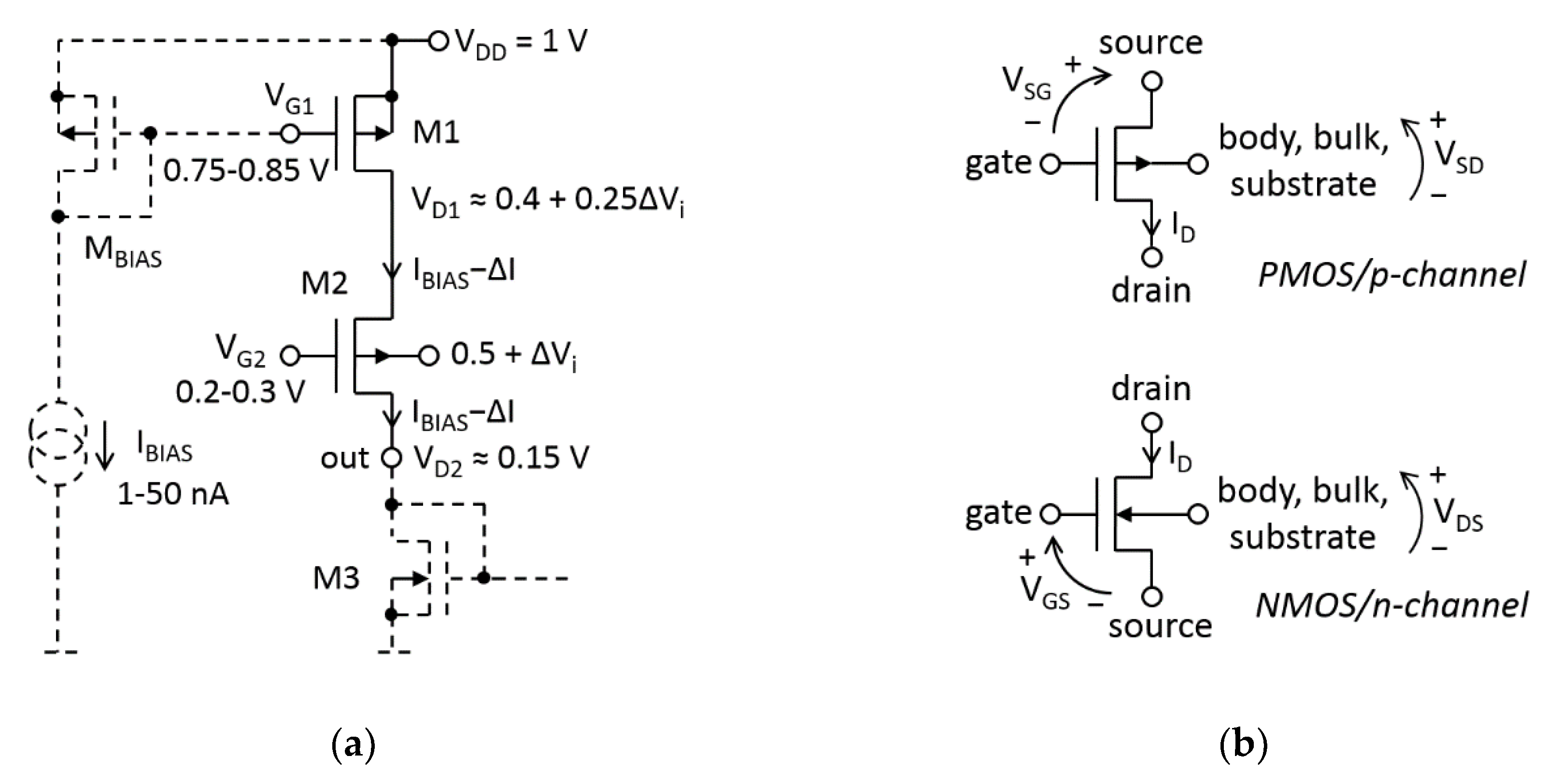
2. Voltage-to-Current Conversion Using Channel-Length-Modulation Effect
2.1. Operation Principles
2.2. Robustness to Unfavorable Factors
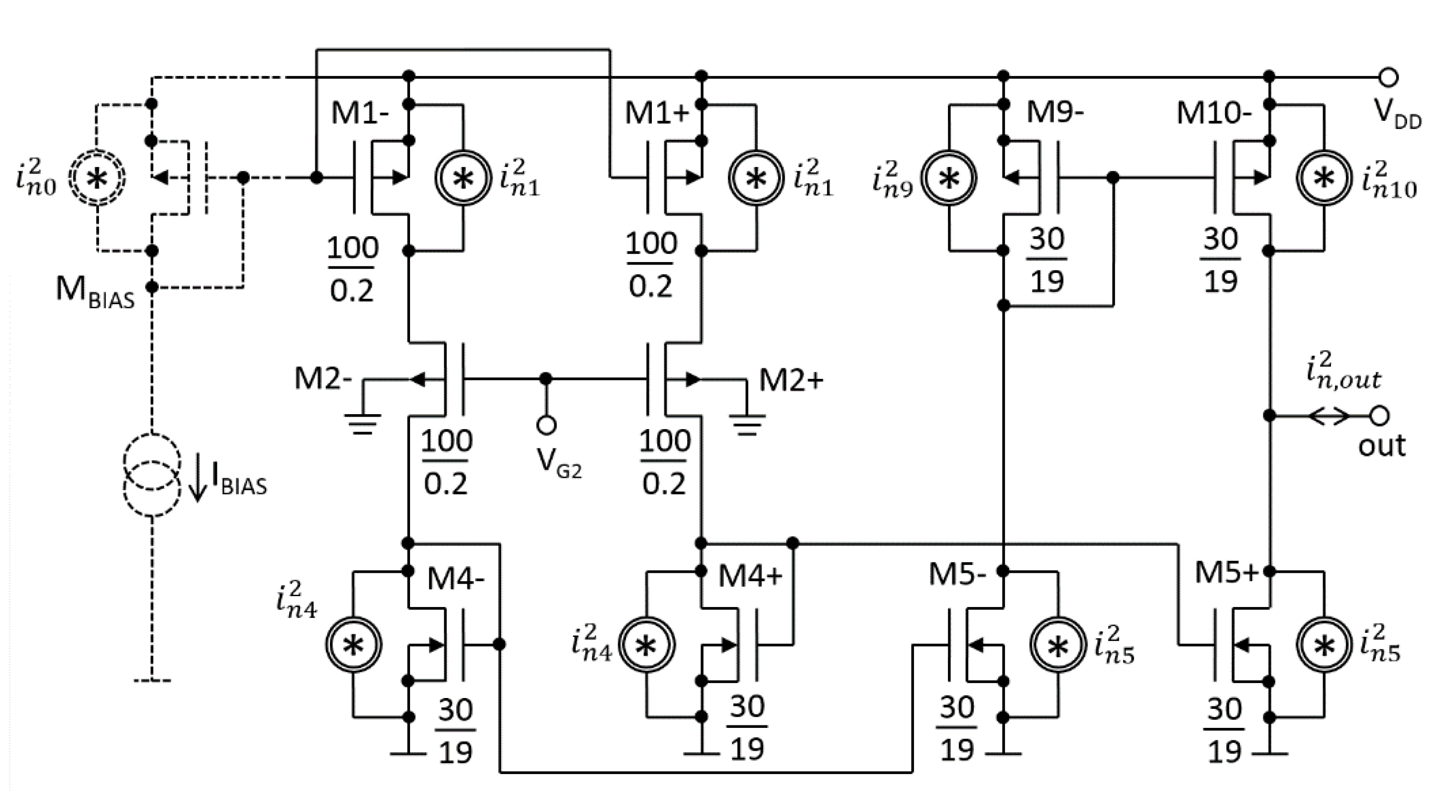
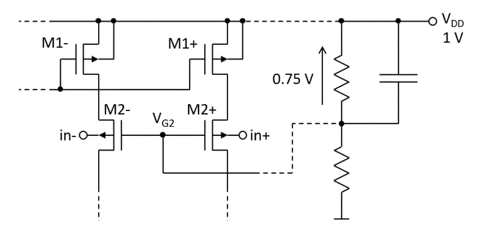
3. Low-Gm OTA (LTA)
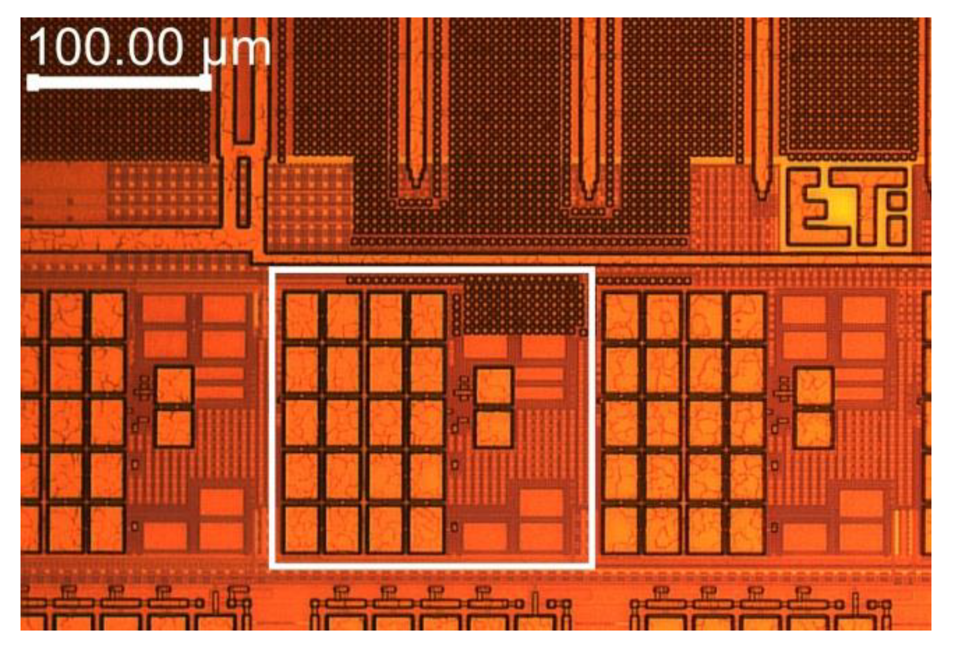
4. Performances of the Prototype
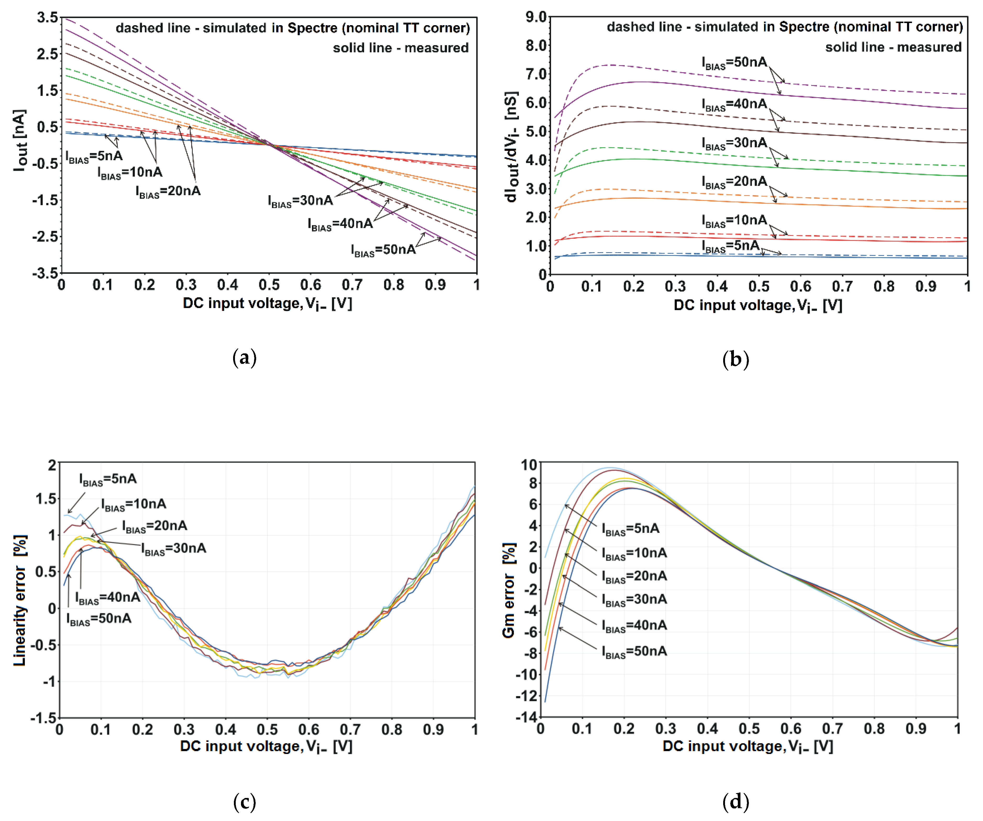
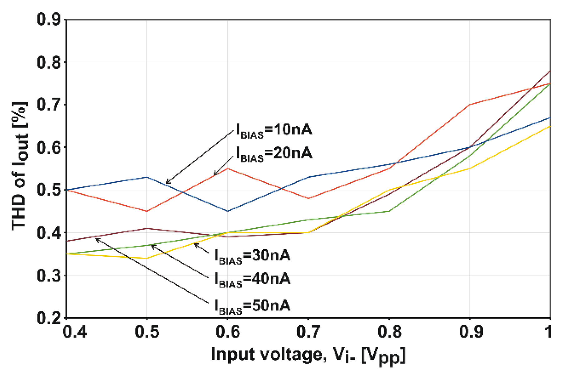
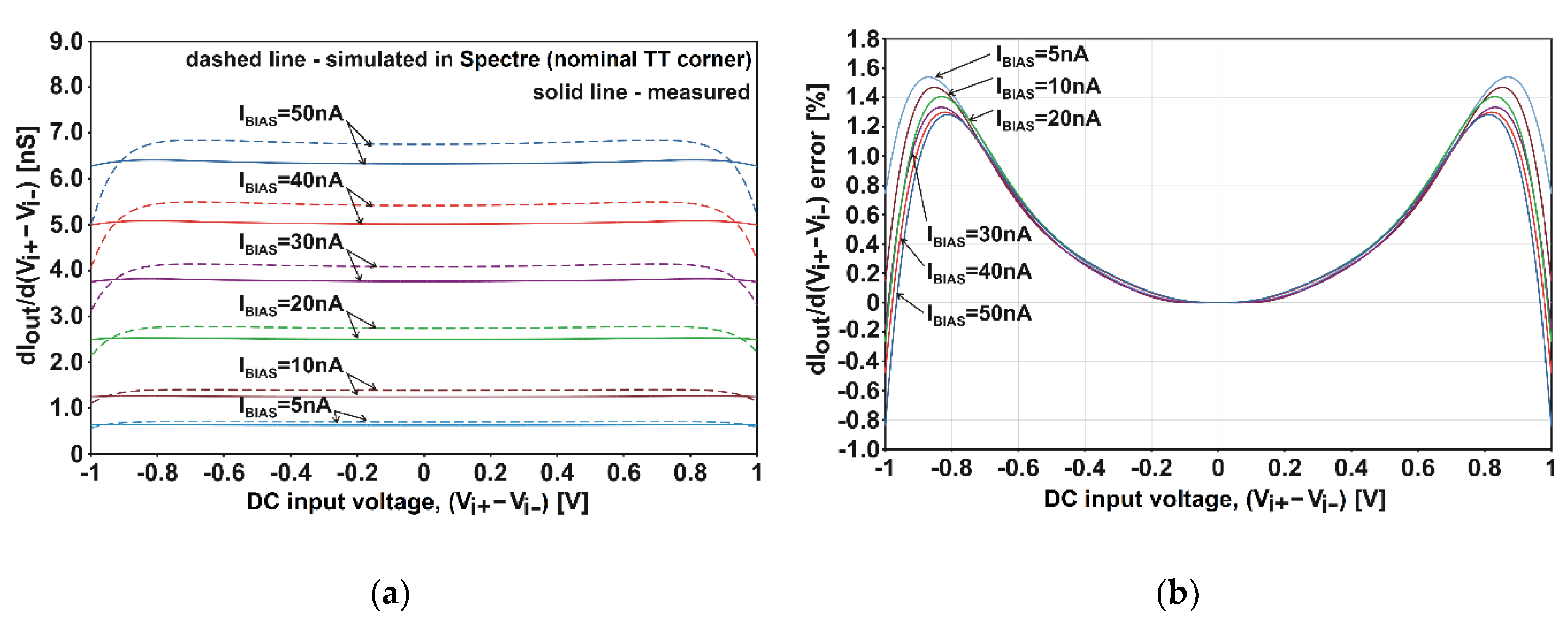
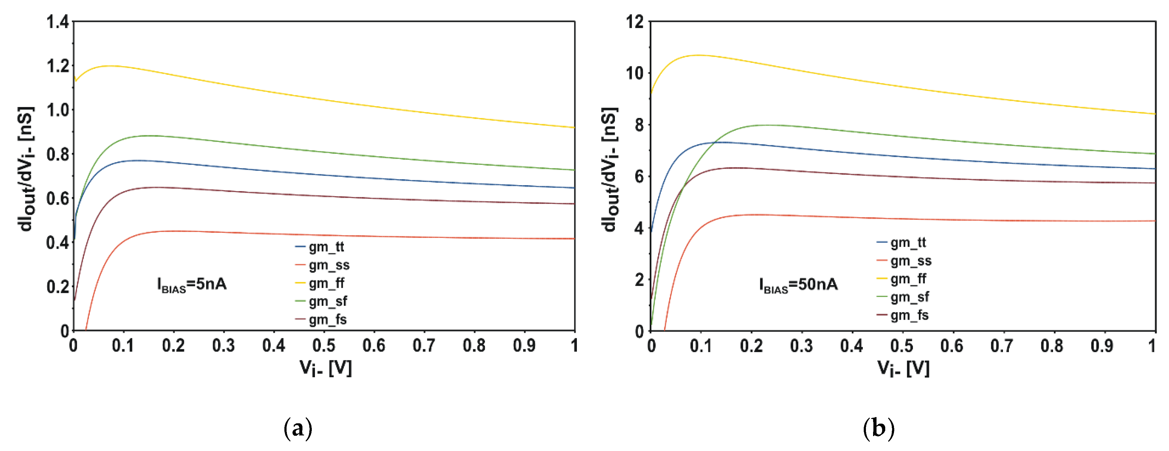
4.1. Linearity of Current-Voltage Characteristics
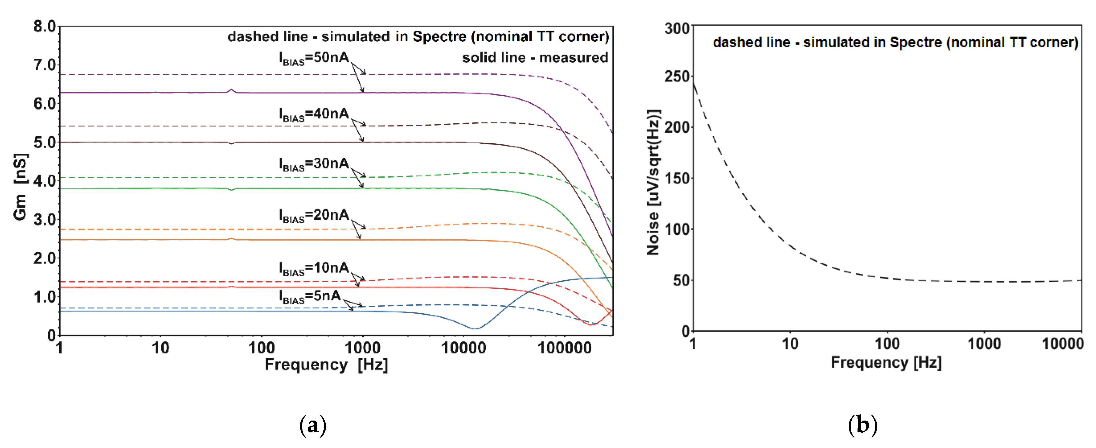
4.2. Frequency and Noise Characteristics
4.3. PSRR and CMRR
4.4. Temperature
4.5. Summary of the Performance Properties
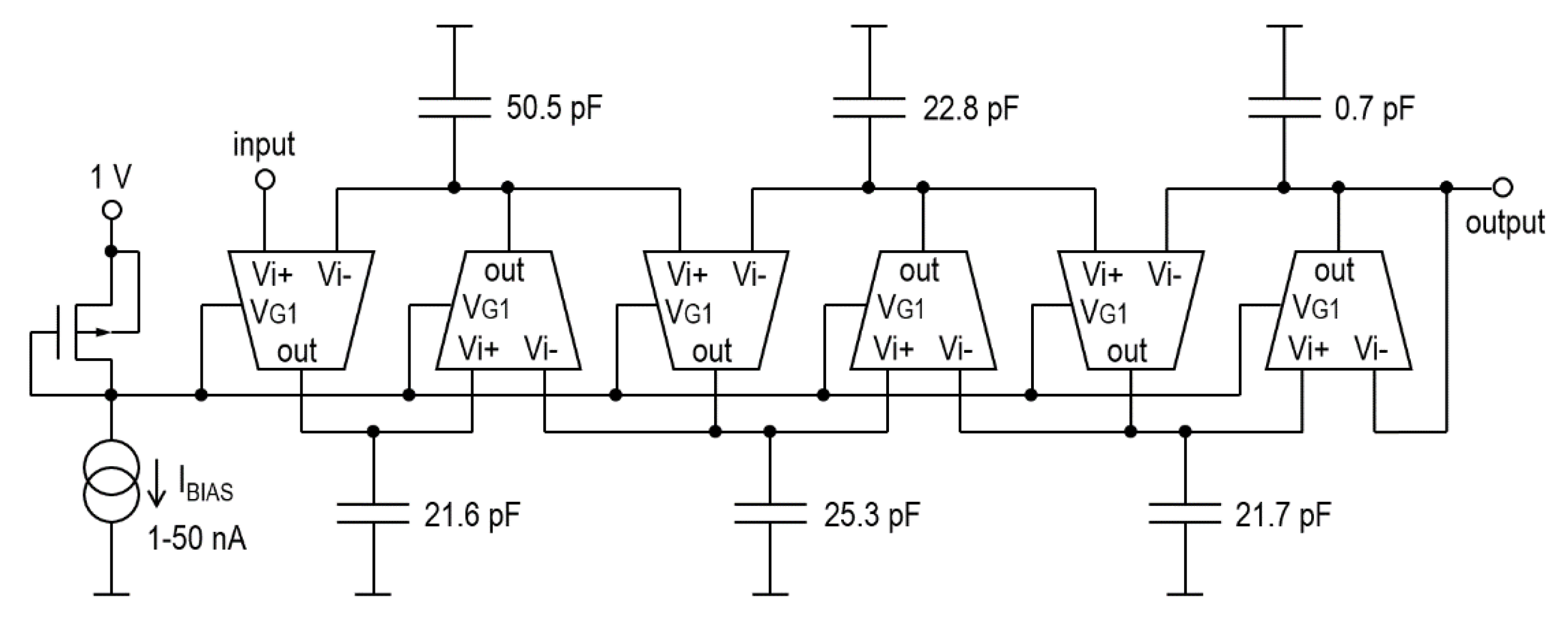
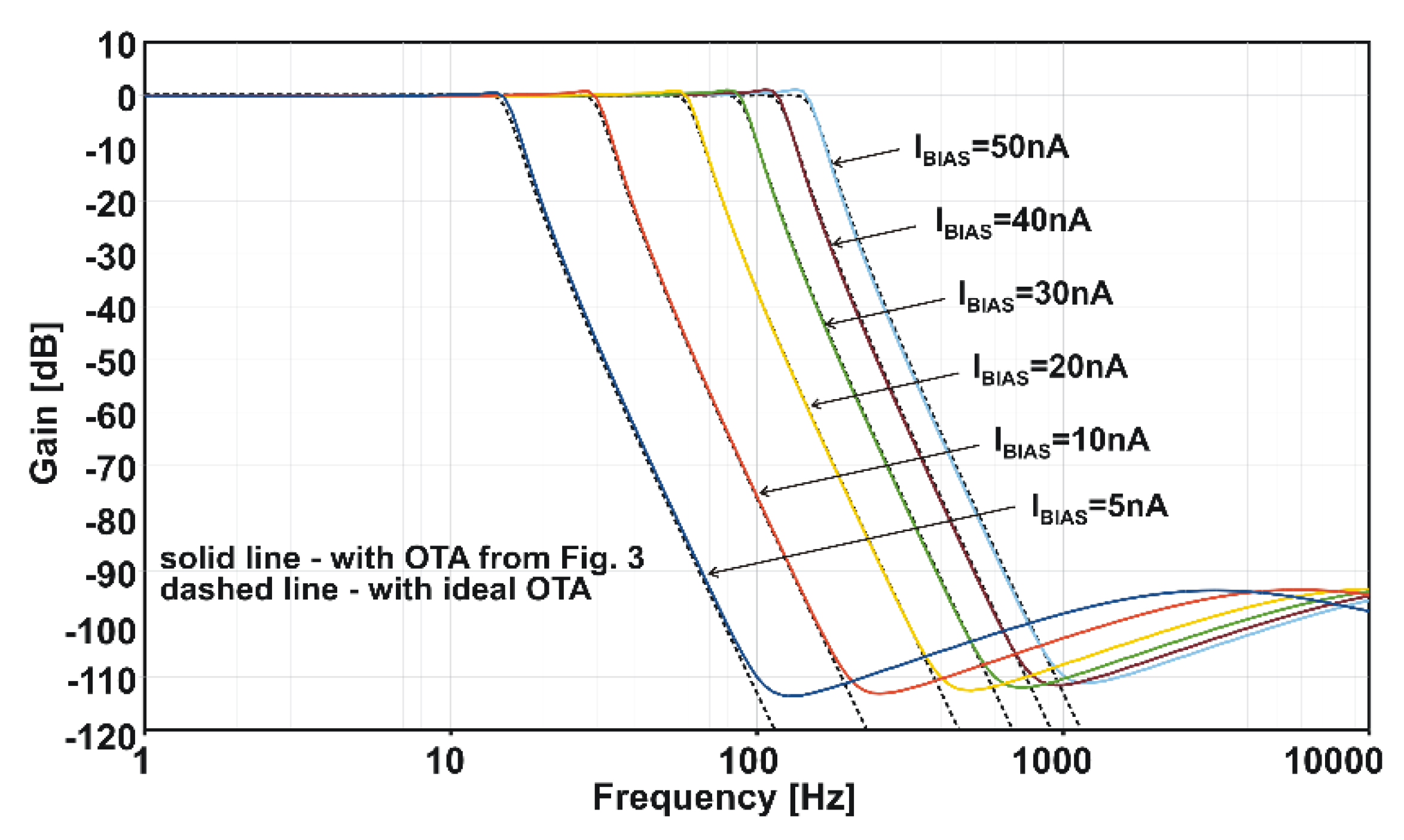
5. Application Example (Simulation Results)
6. Discussion and Conclusions
Author Contributions
Funding
Conflicts of Interest
Appendix A


References
- Zou, X.; Xu, X.; Yao, L.; Lian, Y. A 1-V 450-nW Fully Integrated Programmable Biomedical Sensor Interface Chip. IEEE J. Solid State Circuits 2009, 44, 1067–1077. [Google Scholar] [CrossRef]
- Chou, C.-J.; Kuo, B.-J.; Chen, L.-G.; Hsiao, P.-Y.; Lin, T.-H. A 1-V Low-Noise Readout Front-End for Biomedical Applications in 0.18-μm CMOS. In Proceedings of the 2010 International Symposium on VLSI Design, Automation and Test, Hsin Chu, Taiwan, 26–29 April 2010; pp. 295–298. [Google Scholar] [CrossRef]
- Bohorquez, J.L.; Yip, M.; Chandrakasan, A.P.; Dawson, J.L. A Biomedical Sensor Interface With a sinc Filter and Interference Cancellation. IEEE J. Solid State Circuits 2011, 46, 746–756. [Google Scholar] [CrossRef]
- Harrison, R.R.; Watkins, P.T.; Kier, R.J.; Lovejoy, R.O.; Black, D.J.; Greger, B.; Solzbacher, F. A low-power integrated circuit for a wireless 100-electrode neural recording system. IEEE J. Solid State Circuits 2007, 42, 123–133. [Google Scholar] [CrossRef]
- Chang, C.-H.; Zahrai, S.A.; Wang, K.; Xu, L.; Farah, I.; Onabajo, M. An Analog Front-End Chip with Self-Calibrated Input Impedance for Monitoring of Biosignals via Dry Electrode-Skin Interfaces. IEEE Trans. Circuits Syst. I Reg. Pap. 2017, 64, 2666–2678. [Google Scholar] [CrossRef]
- Yin, M.; Ghovanloo, M. A Low-noise Preamplifier with Adjustable Gain and Bandwidth for Biopotential Recording Applications. In Proceedings of the 2007 IEEE International Symposium on Circuits and Systems, New Orleans, LA, USA, 27–30 May 2007; pp. 321–324. [Google Scholar] [CrossRef]
- Chen, C.-H.; Mak, P.-I.; Zhang, T.-T.; Vai, M.-I.; Mak, P.-U.; Pun, S.-H.; Wan, F.; Martins, R.P. A 2.4 Hz-to-l0 kHz-Tunable Biopotential Filter using a Novel Capacitor Multiplier. In Proceedings of the 2009 Asia Pacific Conference on Postgraduate Research in Microelectronics & Electronics (PrimeAsia), Shanghai, China, 19–21 January 2009; pp. 372–375. [Google Scholar] [CrossRef]
- Liu, Y.-T.; Lie, D.Y.C.; Hu, W.; Nguyen, T. An Ultralow-Power CMOS Transconductor Design with Wide Input Linear Range for Biomedical Applications. In Proceedings of the 2012 IEEE International Symposium on Circuits and Systems (ISCAS), Seoul, Korea, 20–23 May 2012; pp. 2211–2214. [Google Scholar] [CrossRef]
- Lee, Y.-C.; Hsu, W.-Y.; Huang, T.-T.; Chen, H. A Compact Gm-C Filter Architecture with an Ultra-low Corner Frequency and High Ground-noise Rejection. In Proceedings of the 2013 IEEE Biomedical Circuits and Systems Conference (BioCAS), Rotterdam, The Netherlands, 31 October–2 November 2013; pp. 318–321. [Google Scholar] [CrossRef]
- Peng, S.-Y.; Lee, Y.-H.; Wang, T.-Y.; Huang, H.-C.; Lai, M.-R.; Lee, C.-H.; Liu, L.-H. A Power-Efficient Reconfigurable OTA-C Filter for Low-Frequency Biomedical Applications. IEEE Trans. Circuits Syst. I Reg. Pap. 2018, 65, 543–555. [Google Scholar] [CrossRef]
- Pérez-Bailón, J.; Calvo, B.; Medrano, N. A CMOS Low Pass Filter for SoC Lock-in-Based Measurement Devices. Sensors 2019, 19, 5173. [Google Scholar] [CrossRef] [PubMed]
- Veeravalli, A.; Sanchez-Sinencio, E.; Silva-Martnez, J. Transconductance amplifier structures with very small transconductances: A comparative design approach. IEEE J. Solid State Circuits 2002, 37, 770–775. [Google Scholar] [CrossRef]
- Arnaud, A.; Fiorelli, R.; Galup-Montoro, C. Nanowatt, Sub-nS OTAs, With Sub-10-mV Input Offset, Using Series-Parallel Current Mirrors. IEEE J. Solid State Circuits 2006, 41, 2009–2018. [Google Scholar] [CrossRef]
- Yodtean, A.; Thanachayanont, A. Sub 1-V highly-linear low-power class-AB bulk-driven tunable CMOS transconductor. Analog Integr. Circuits Signal Process. 2013, 75, 383–397. [Google Scholar] [CrossRef]
- Cotrim, E.D.C.; Ferreira, L.H.D. An ultra-low-power CMOS symmetrical OTA for low-frequency Gm-C applications. Analog Integr. Circuits Signal Process. 2012, 71, 275–282. [Google Scholar] [CrossRef]
- Soares, C.F.T.; de Moraes, G.S.; Petraglia, A. A low-transconductance OTA with improved linearity suitable for low-frequency Gm-C filters. Microelectron. J. 2014, 45, 1499–1507. [Google Scholar] [CrossRef]
- El Mourabit, A.; Lu, G.-N.; Pittet, P. Wide-linear-range subthreshold OTA for low-power, low-Voltage, and low-frequency applications. IEEE Trans. Circuits Syst. I Reg. Pap. 2005, 52, 1481–1488. [Google Scholar] [CrossRef]
- Huang, Y.; Drakakis, E.M.; Toumazou, C. A 30pA/V–25 µA/V linear CMOS channel-length-modulation OTA. Microelectron. J. 2009, 40, 1458–1465. [Google Scholar] [CrossRef]
- Laker, K.R.; Sansen, W.M.C. Design of Analog Integrated Circuits and Systems; McGraw-Hill: New York, NY, USA, 1994. [Google Scholar]
- Tsividis, Y.P. Operation and Modeling of the MOS Transistor, 2nd ed.; Oxford University Press: New York, NY, USA, 1999. [Google Scholar]
- Carusone, T.C.; Johns, D.A.; Martin, K.W. Frequency Response of Elementary Transistor Circuits. In Analog Integrated Circuit Design, 2nd ed.; John Wiley & Sons, Inc.: Hoboken, NJ, USA, 2012. [Google Scholar]
- Carusone, T.C.; Johns, D.A.; Martin, K.W. Noise and Linearity Analysis and Modelling. In Analog Integrated Circuit Design, 2nd ed.; John Wiley & Sons, Inc.: Hoboken, NJ, USA, 2012. [Google Scholar]
- Szczepanski, S.; Pankiewicz, B.; Koziel, S.; Wojcikowski, M. Multiple output differential OTA with linearized bulk driven active-error feedback loop for continuous time filter applications. Int. J. Circuit Theory Appl. 2015, 43, 1671–1686. [Google Scholar] [CrossRef]
- Allen, P.E.; Holberg, D.R. Bandgap Reference. In CMOS Analog Circuit Design, 2nd ed.; Oxford University Press: New York, NY, USA, 2002. [Google Scholar]
- Zhang, J.; Chan, S.-C.; Li, H.; Zhang, N.; Wang, L. An Area-Efficient and Highly Linear Reconfigurable Continuous-Time Filter for Biomedical Sensor Applications. Sensors 2020, 20, 2065. [Google Scholar] [CrossRef] [PubMed]
- Thanapitak, S.; Sawigun, C.A. Subthreshold Buffer-Based Biquadratic Cell and its Application to Biopotential Filter Design. IEEE Trans. Circuits Syst. I Reg. Pap. 2018, 65, 2774–2783. [Google Scholar] [CrossRef]
- Sawigun, C.; Thanapitak, S.A. Nanopower Biopotential Lowpass Filter Using Subthreshold Current-Reuse Biquads With Bulk Effect Self-Neutralization. IEEE Trans. Circuits Syst. I Reg. Pap. 2018, 66, 1746–1757. [Google Scholar] [CrossRef]
- Krishna, J.R.M.; Laxminidhi, T. Widely tunable low-pass gm-C filter for biomedical applications. IET Circuits Devices Syst. 2019, 13, 239–244. [Google Scholar] [CrossRef]
- Lee, S.-Y.; Cheng, C.-J. Systematic design and modeling of OTA-C filter for portable ECG detection. IEEE Trans. Biomed. Circuits Syst. I 2009, 3, 53–64. [Google Scholar] [CrossRef] [PubMed]
- Bano, S.; Narejo, G.B.; Ali Shah, S.M.U. Power Efficient Fully Differential Bulk Driven OTA for Portable Biomedical Application. Electronics 2018, 7, 41. [Google Scholar] [CrossRef]
- Qian, C.; Parramon, J.; Sanchez-Sinencio, E. A micro power low-noise neural recording front-End circuit for epileptic seizure detection. IEEE J. Solid State Circuits 2011, 46, 1392–1405. [Google Scholar] [CrossRef]


| Parameter | Simulated | Measured |
|---|---|---|
| Technology/Vendor | Standard 180 nm CMOS 1P6M/TSMC | |
| Physical dimensions 1 | 174 µm × 156 µm | |
| Supply voltage VDD | 1 V (min. 0.8 V, max. 1.8 V) | |
| Average current consumption 1 | 32–290 nA | 28–270 nA |
| Gm tuning range (IBIAS range 5–50 nA) | 0.7–6.75 nS | 0.62–6.28 nS |
| Gm temperature drift 2 | 2.1 pS/°C @ IBIAS = 5 nA 9.7 pS/°C @ IBIAS = 50 nA | - - |
| Input common-mode range | 0.1–1 V | 0–1 V (rail-to-rail) |
| THD of Iout non-symmetrical driving symmetrical driving | 2.4% @ 1 Vpp, 1% @ 0.64 Vpp 0.47% @ 2.0 Vpp | 0.8% @ 1 Vpp 0.18% @ 2 Vpp |
| Gm deviation (linearity) error non-symmetrical driving symmetrical driving | ±22% @ 1 Vpp ±12% @ 2 Vpp | ±12% @ 1 Vpp ±1.5% @ 2 Vpp |
| Input-reffered noise | 760 µVRMS (integrated over 1–100 Hz) | - |
| Signal to noise ratio (SNR) non-symmetrical driving symmetrical driving | 49.5 dB @ THD = 1% 59.3 dB @ THD = 0.47% | - - |
| CMRR, PSRR | min. 56 dB, 47 dB 3 | min. 57 dB, 48 dB 4 |
| Input offset voltage (VOS) | max. ± 25 mV 3 | 25–50 mV 4 |
| Mismatch-induced deviation of Gm | max. ± 4.5% 3 | - |
| Parameter | This Work | [12] (BD+CD Case) | [16] (Simulated) | [17] | [18] |
|---|---|---|---|---|---|
| Type of input/output | diff./single | diff./single | diff./diff. | diff./single | diff./diff. |
| Gm | 0.62–6.28 nS | 9.4 nS | 39.5–367.2 nS | 0.46–82 nS | 30 pS–25 µS |
| Supply voltage | 1 V | 2.7 V (±1.35 V) | 5 V (±2.5 V) | 1.5 V | 5 V (±2.5 V) |
| Power consumption | <0.3 µW (28–270 nW) | 4.05 µW (sim.) | 160 µW | <1 µW | <300 µW |
| Input comm.-mode range | rail-to-rail | - | - | rail-to-rail | - |
| Linear range for symmetrical input | 2 Vpp @ 0.18% THD | 0.9 Vpp @ 1% HD3 | 2 Vpp @ 0.13% THD | 1.2 Vpp @ 1% THD | 2.6 Vpp @ 1% THD |
| Input-referred noise | 760 µVRMS (sim.) (1–100 Hz) | 104.7 µVRMS (0.01–10 Hz) | 332 µVRMS (10–30 kHz) | 110 µVRMS (1–100 Hz) | 635 µVRMS (1 Hz–2 MHz) |
| SNR | 59.3 dB (sim.) @ 0.47% THD | 69.6 dB @ 1% HD3 | ~66.5 dB @ 0.13% THD | 70 dB @ 1% THD | 62 dB @ 1% THD |
| CMRR/PSRR | 56 dB/47 dB | - | >44.8 dB/n.a. | - | >80 dB/>80 dB |
| CMOS process | 0.18 µm | 1.2 µm | 0.35 µm | 0.8 µm | 0.35 µm |
| Layout area | 0.027 mm2 | 0.22 mm2 | 0.006 mm2 | 0.04 mm2 | 0.046 mm2 |
© 2020 by the authors. Licensee MDPI, Basel, Switzerland. This article is an open access article distributed under the terms and conditions of the Creative Commons Attribution (CC BY) license (http://creativecommons.org/licenses/by/4.0/).
Share and Cite
Jakusz, J.; Jendernalik, W.; Blakiewicz, G.; Kłosowski, M.; Szczepański, S. A 1-nS 1-V Sub-1-µW Linear CMOS OTA with Rail-to-Rail Input for Hz-Band Sensory Interfaces. Sensors 2020, 20, 3303. https://doi.org/10.3390/s20113303
Jakusz J, Jendernalik W, Blakiewicz G, Kłosowski M, Szczepański S. A 1-nS 1-V Sub-1-µW Linear CMOS OTA with Rail-to-Rail Input for Hz-Band Sensory Interfaces. Sensors. 2020; 20(11):3303. https://doi.org/10.3390/s20113303
Chicago/Turabian StyleJakusz, Jacek, Waldemar Jendernalik, Grzegorz Blakiewicz, Miron Kłosowski, and Stanisław Szczepański. 2020. "A 1-nS 1-V Sub-1-µW Linear CMOS OTA with Rail-to-Rail Input for Hz-Band Sensory Interfaces" Sensors 20, no. 11: 3303. https://doi.org/10.3390/s20113303
APA StyleJakusz, J., Jendernalik, W., Blakiewicz, G., Kłosowski, M., & Szczepański, S. (2020). A 1-nS 1-V Sub-1-µW Linear CMOS OTA with Rail-to-Rail Input for Hz-Band Sensory Interfaces. Sensors, 20(11), 3303. https://doi.org/10.3390/s20113303