Integrated Circuit Design for Radiation-Hardened Charge-Sensitive Amplifier Survived up to 2 Mrad

Abstract
1. Introduction
2. Total Ionizing Dose Effects on MOSFET and BJT
2.1. Threshold Voltage Shift of MOSFET
2.2. Noise Analysis Based on MOSFET
2.3. Gain Degradation of BJT
2.4. Noise Analysis Based on BJT
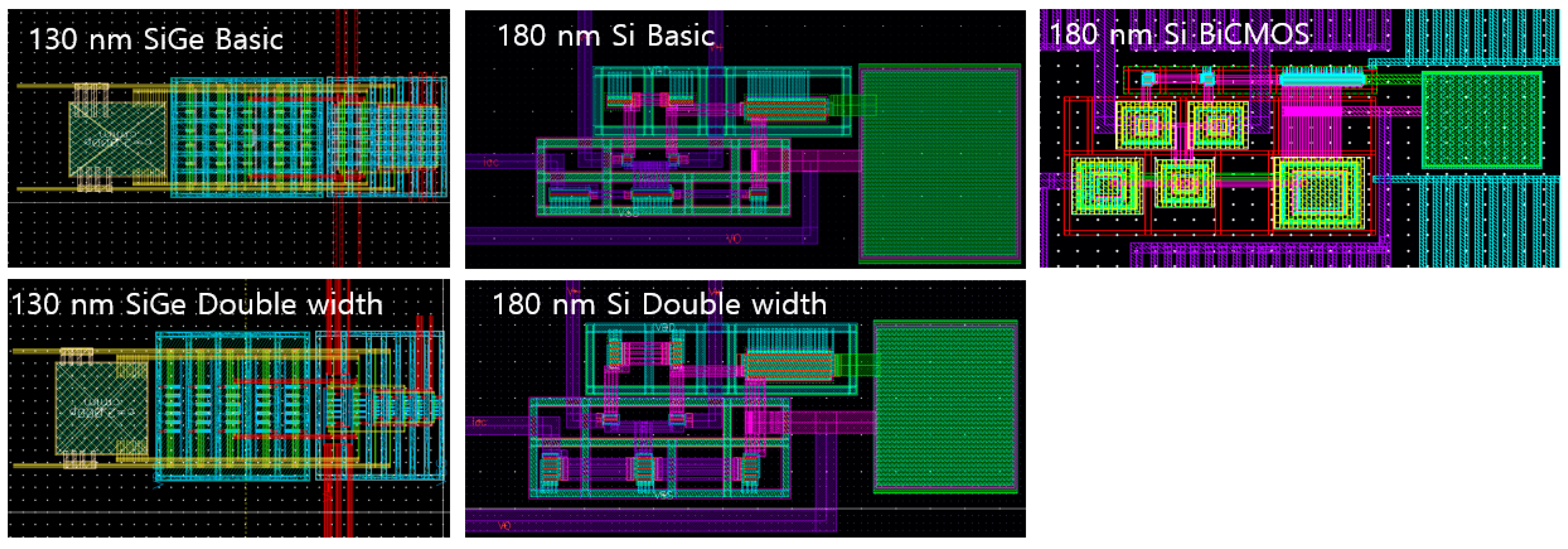
3. Designed Charge-Sensitive Amplifier
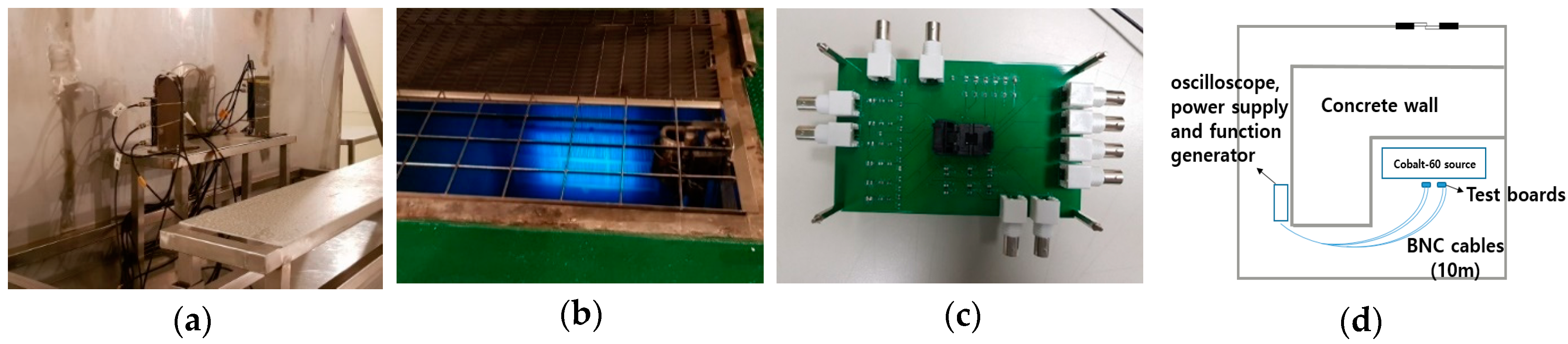
4. Experimental Setup
5. Experimental Results
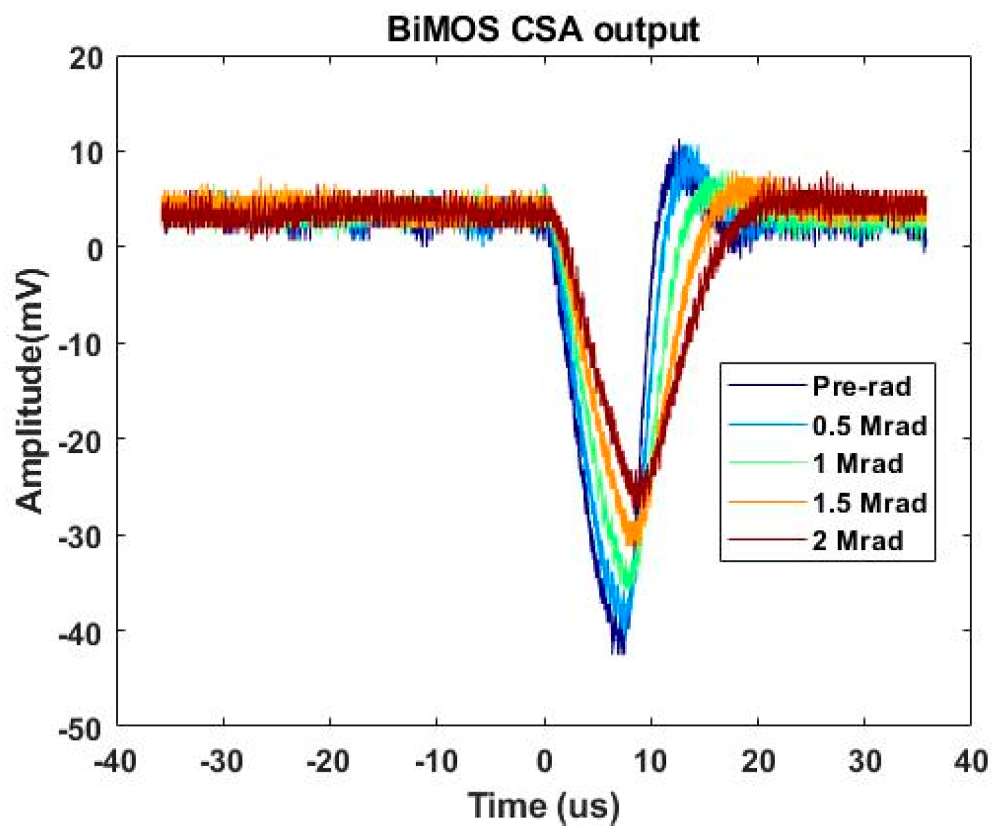
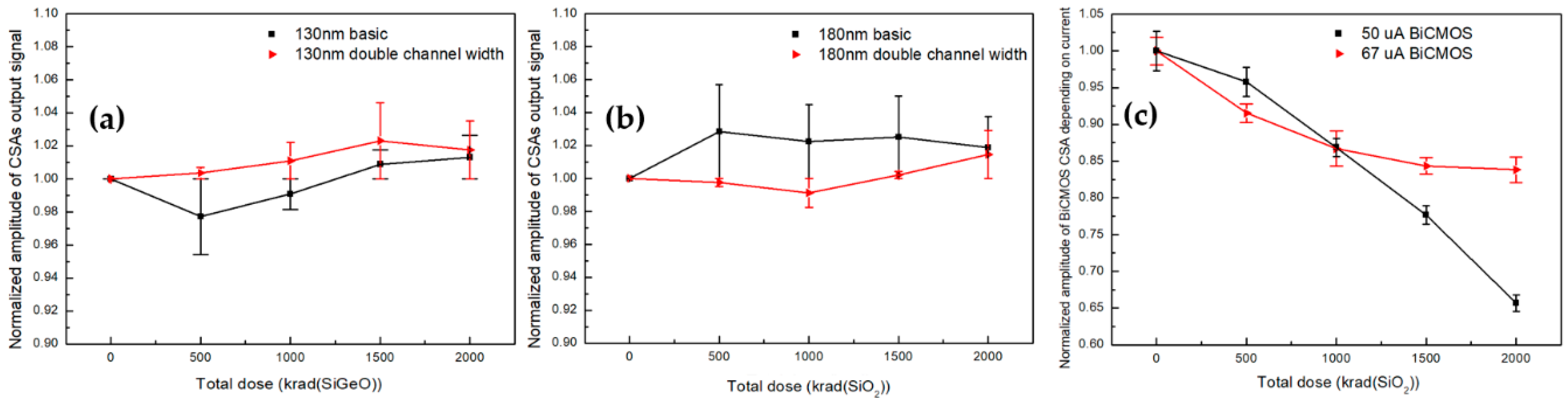
5.1. Normalized Amplitude
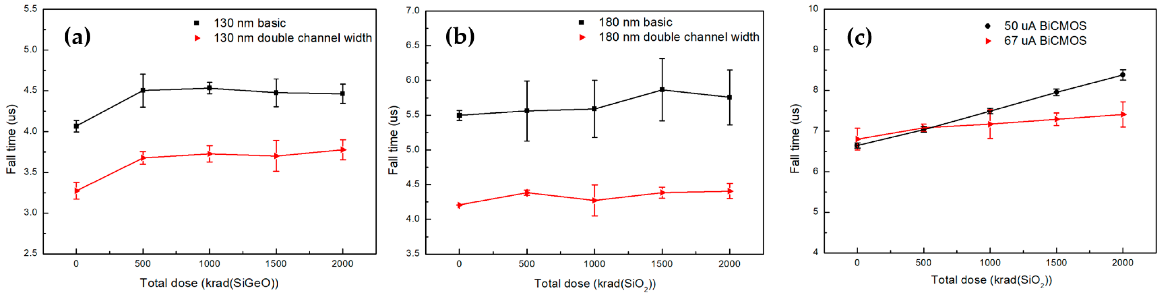
5.2. Fall Time
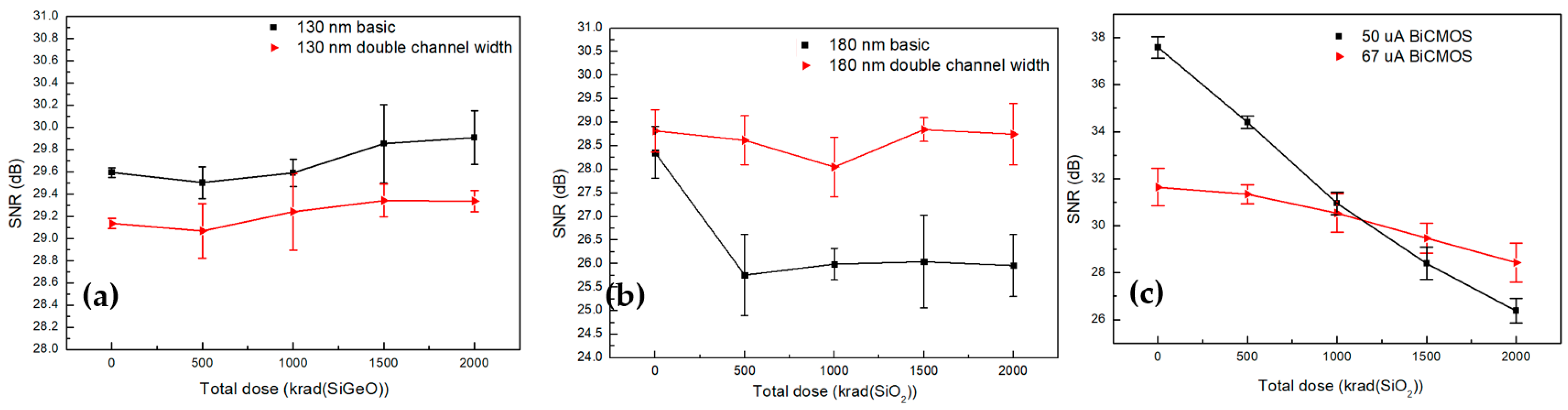
5.3. SNR
6. Conclusions
Author Contributions
Funding
Conflicts of Interest
References
- McGregor, D.S.; Ohmes, M.F.; Ortiz, R.E.; Sabbir Ahmed, A.S.M.; Kenneth Shultis, J. Micro-pocket fission detectors (MPFD) for in-core neutron flux monitoring. Nucl. Instrum. Methods Phys. Res. Sect. A Accel. Spectrometers, Detect. Assoc. Equip. 2005, 554, 494–499. [Google Scholar] [CrossRef]
- Girard, S.; Kuhnhenn, J.; Gusarov, A.; Brichard, B.; Van Uffelen, M.; Ouerdane, Y.; Boukenter, A.; Marcandella, C. Radiation Effects on Silica-Based Optical Fibers: Recent Advances and Future Challenges. IEEE Trans. Nucl. Sci. 2013, 60, 2015–2036. [Google Scholar] [CrossRef]
- Anderson, M.; Gao, F.; Knipper, K.; Hain, C.; Dulaney, W.; Baldocchi, D.; Eichelmann, E. Field-Scale Assessment of Land and Water Use Change over the California Delta Using Remote Sensing. Remote. Sens. 2018, 10, 889. [Google Scholar] [CrossRef]
- Endland, T.D.; Diestelhorst, R.M.; Kenyon, E.W.; Cressler, J.D. A new approach to designing electronic systems for operation in extreme environments: Part II – The SiGe remote electronics unit. IEEE Aerosp. Electron. Syst. Mag. 2012, 27, 29–41. [Google Scholar] [CrossRef]
- Re, V.; Manghisoni, M.; Ratti, L.; Speziali, V.; Traversi, G. Total ionizing dose effects on the noise performances of a 0.13 um CMOS technology. IEEE Trans. Nucl. Sci. 2006, 53, 1599–1606. [Google Scholar] [CrossRef]
- Fleetwood, Z.E.; Kenyon, E.W.; Lourenco, N.E.; Jain, S.; Zhang, E.X.; England, T.D.; Cressler, J.D.; Schrimpf, R.D.; Fleetwood, D.M. Advanced SiGe BiCMOS Technology for Multi-Mrad Electronic Systems. IEEE Trans. Device Mater. Reliab. 2014, 14, 844–848. [Google Scholar] [CrossRef]
- Manghisoni, M.; Ratti, L.; Re, V.; Speziali, V.; Traversi, G.; Candelori, A. Comparison of ionizing radiation effects in 0.18 and 0.25 μm CMOS technologies for analog applications. IEEE Trans. Nucl. Sci. 2003, 50, 1827–1833. [Google Scholar] [CrossRef]
- Schwank, J.R.; Shaneyfelt, M.R.; Fleetwood, D.M.; Felix, J.A.; Dodd, P.E.; Paillet, P.; Ferlet-Cavrois, V. Radiation Effects in MOS Oxides. IEEE Trans. Nucl. Sci. 2008, 55, 1833–1853. [Google Scholar] [CrossRef]
- Fleetwood, D.M. Total Ionizing Dose Effects in MOS and Low-Dose-Rate-Sensitive Linear-Bipolar Devices. IEEE Trans. Nucl. Sci. 2013, 60, 1706–1730. [Google Scholar] [CrossRef]
- Saks, N.S.; Ancona, M.G.; Modolo, J.A. Generation of interface states by ionizing radiation in very thin MOS oxides. IEEE Trans. Nucl. Sci. 1986, 33, 1185–1190. [Google Scholar] [CrossRef]
- Gromov, V.; Annema, A.J.; Kluit, R.; Visschers, J.L.; Timmer, P. A Radiation Hard Bandgap Reference Circuit in a Standard 0.13 μm CMOS Technology. IEEE Trans. Nucl. Sci. 2007, 54, 2727–2733. [Google Scholar] [CrossRef]
- Boufouss, E.H.; Francis, L.A.; Kilchytska, V.; Gerard, P.; Simon, P.; Flandre, D. Ultra-Low Power High Temperature and Radiation Hard Complementary Metal-Oxide-Semiconductor (CMOS) Silicon-on-Insulator (SOI) Voltage Reference. Sensors 2013, 13, 17265–17280. [Google Scholar] [CrossRef] [PubMed]
- Wang, C.; Hu, S.; Gao, C.; Feng, C. Nuclear Radiation Degradation Study on HD Camera Based on CMOS Image Sensor at Different Dose Rates. Sensors 2018, 18, 514. [Google Scholar] [CrossRef] [PubMed]
- Ro, D.; Min, C.; Chang, I.J.; Lee, H.M. A Radiation-Hardened SAR ADC with Delay-Based Dual Feedback Flip-Flops for Sensor Readout Systems. Sensors 2020, 20, 171. [Google Scholar] [CrossRef] [PubMed]
- Mossawir, B.; Linscott, I.R.; Inan, U.S.; Roeder, J.L.; Osborn, J.V.; Witczak, S.C.; King, E.E.; LaLumondiere, S.D. A TID and SEE Radiation-Hardened, Wideband, Low-Noise Amplifier. IEEE Trans. Nucl. Sci. 2006, 53, 3439–3448. [Google Scholar] [CrossRef]
- Xu, K.; Chen, Y.; Okhal, T.A.; Snyman, L.W. Micro optical sensors based on avalanching silicon light-emitting devices monolithically integrated on chips. Opt. Mater. Express 2019, 9, 3985–3997. [Google Scholar] [CrossRef]
- Zhang, L.; Dong, T. A Si/SiGe quantum well based biosensor for direct analysis of exothermic biochemical reaction. J. Micromech. Microeng. 2013, 23, 9. [Google Scholar] [CrossRef]
- Kim, H.S.; Han, S.W.; Yang, J.H.; Kim, S.; Kim, Y.; Kim, S.; Yoon, D.K.; Lee, J.S.; Park, J.C.; Sung, Y.; et al. An asynchronous sampling-based 128 × 128 direct photon-counting X-ray image detector with multi-energy discrimination and high spatial resolution. IEEE J. Solid-State Circuits 2013, 48, 541–558. [Google Scholar] [CrossRef]
- Grybos, P.; Szczygiel, R. Pole-Zero Cancellation Circuit With Pulse Pile-Up Tracking System for Low Noise Charge-Sensitive Amplifiers. IEEE Trans. Nucl. Sci. 2008, 55, 583–590. [Google Scholar] [CrossRef]
- Kwon, I.; Kang, T.; Hammig, M.D. Experimental Validation of Charge-Sensitive Amplifier Configuration that Compensates for Detector Capacitance. IEEE Trans. Nucl. Sci. 2016, 63, 1202–1208. [Google Scholar] [CrossRef]
- Nalwa, H.S. Silicon-Based Material and Devices, Two-Volume Set: Materials and Processing, Properties and Devices, 1st ed.; ACADEMIC PRESS: Cambridge, MA, USA, 2001; pp. 110–113. [Google Scholar]
- Timp, G.; Bude, J.; Baumann, F.; Bourdelle, K.K. The relentless march of the MOSFET gate oxide thickness to zero. Microelectron. Reliab. 2000, 40, 557–562. [Google Scholar] [CrossRef]
- Babcock, J.A.; Loftin, B.; Madhani, P.; Pinto, A.; Schroder, D.K. Comparative low frequency noise analysis of bipolar and MOS transistors using an advanced complementary BiCMOS technology. In Proceedings of the IEEE 2001 Custom Integrated Circuits Conference (Cat. No.01CH37169), San Diego, CA, USA, 9 May 2001; pp. 385–388. [Google Scholar] [CrossRef]
- Sedra, A.S.; Smith, K.C. Microelectronic Circuits, 7th ed.; OXFORD UNIVERSITY PRESS: New York, NY, USA, 2004; pp. 305–318. [Google Scholar]
- Wilamowski, B.M.; David Irwin, J. Fundamentals of Industrial Electronics, 1st ed.; CRC Press: Boca Raton, FL, USA, 2011. [Google Scholar]
- Babcock, J.A.; Cressler, J.D.; Vempati, L.S.; Jaeger, R.C.; Clark, S.D.; Harame, D.L. Ionizing Radiation Tolerance and Low—frequency Noise Degradation in UHV/CVD SiGe HBT’s. IEEE Electron Device Lett. 1995, 16, 351–353. [Google Scholar] [CrossRef]
- European Space Components coordination. Total Dose Steady-State Irradiation Test Method; Basic Specification NO. 22900; European Space Agency: Paris, France, 2016; p. 10. [Google Scholar]
- Xu, K. Silicon MOS Optoelectronic Micro-Nano Structure Based on Reverse-Biased PN Junction. Phys. Status Solidi A 2019, 216, 1800868. [Google Scholar] [CrossRef]
- Gu, Y.; Yuan, J.S. Gate-Oxide Thickness Effects on Hot-Carrier-Induced Degradation in n-MOSFETs. Int. J. Electron. 1998, 85, 1–9. [Google Scholar] [CrossRef]
- Faccio, F.; Michelis, S.; Cornale, D.; Paccagnella, A.; Gerardin, S. Radiation-Induced Short Channel (RISCE) and Narrow Channel (RINCE) Effects in 65 and 130 nm MOSFETs. IEEE Trans. Nucl. Sci. 2015, 62, 2933–2940. [Google Scholar] [CrossRef]
- Faccio, F.; Cervelli, G. Radiation-induced edge effects in deep submicron CMOS transistors. Nucl. Sci. IEEE Trans. 2005, 52, 2413–2420. [Google Scholar] [CrossRef]
- Manghisoni, M.; Ratti, L.; Re, V.; Speziali, V. Submicron CMOS technologies for low-noise analog front-end circuits. IEEE Trans. Nucl. Sci. 2002, 49, 1783–1790. [Google Scholar] [CrossRef]


| Variable CSA | 130 nm SiGe CMOS | 130 nm SiGe CMOS | 180 nm Si CMOS | 180 nm Si CMOS | 180 nm Si BiCMOS | 180 nm Si BiCOMS |
|---|---|---|---|---|---|---|
| Basic | Double Width | Basic | Double Width | Tail Current 50 μA | Tail Current 67 μA | |
| and W/L (µm) | 1/0.13 | 2/0.13 | 1/0.18 | 2/0.18 | 2/2 | 2/2 |
| W/L (µm) | 4/0.13 | 8/0.13 | 4/0.18 | 8/0.18 | 2/2 | 2/2 |
| and W/L (µm) | 3/0.13 | 6/0.13 | 3/0.18 | 6/0.18 | 10/0.18 | 10/0.18 |
| Gate oxide thickness (nm) | 2 | 2 | 3.6 | 3.6 | 3.7 | 3.7 |
| Shallow Trench Isolation (nm) | 400 | 400 | 350 | 350 | 320 | 320 |
| Gain (dB) | 41.9 | 42.3 | 39.37 | 38.83 | 62.43 | 62.43 |
| Gain Bandwidth Product (MHz) | 316.2 | 377.3 | 202.25 | 289.5 | 115.24 | 115.24 |
| Phase Margin (˚) | 56.46 | 57.6 | 58.72 | 57.5 | 44.2 | 44.2 |
| Variable CSA | 130 nm SiGe CMOS | 130 nm SiGe CMOS | 180 nm Si CMOS | 180 nm Si CMOS | 180 nm Si BiCMOS | 180 nm Si BiCMOS |
|---|---|---|---|---|---|---|
| Basic | Double Width | Basic | Double Width | Tail Current 50 μA | Tail Current 67 μA | |
| Amplitude variation (%) () | 3.6 | 2.23 | 2.85 | 2.32 | 34.3 | 16.17 |
| Fall time variation (ns) () | −398 | −504 | −260 | −210 | −1730 | −608 |
| SNR (dB) () | −0.314 | −0.202 | 2.396 | 0.07 | 11.6 | 3.12 |
© 2020 by the authors. Licensee MDPI, Basel, Switzerland. This article is an open access article distributed under the terms and conditions of the Creative Commons Attribution (CC BY) license (http://creativecommons.org/licenses/by/4.0/).
Share and Cite
Lee, C.; Cho, G.; Unruh, T.; Hur, S.; Kwon, I. Integrated Circuit Design for Radiation-Hardened Charge-Sensitive Amplifier Survived up to 2 Mrad. Sensors 2020, 20, 2765. https://doi.org/10.3390/s20102765
Lee C, Cho G, Unruh T, Hur S, Kwon I. Integrated Circuit Design for Radiation-Hardened Charge-Sensitive Amplifier Survived up to 2 Mrad. Sensors. 2020; 20(10):2765. https://doi.org/10.3390/s20102765
Chicago/Turabian StyleLee, Changyeop, Gyuseong Cho, Troy Unruh, Seop Hur, and Inyong Kwon. 2020. "Integrated Circuit Design for Radiation-Hardened Charge-Sensitive Amplifier Survived up to 2 Mrad" Sensors 20, no. 10: 2765. https://doi.org/10.3390/s20102765
APA StyleLee, C., Cho, G., Unruh, T., Hur, S., & Kwon, I. (2020). Integrated Circuit Design for Radiation-Hardened Charge-Sensitive Amplifier Survived up to 2 Mrad. Sensors, 20(10), 2765. https://doi.org/10.3390/s20102765