A High-Performance 2.5 μm Charge Domain Global Shutter Pixel and Near Infrared Enhancement with Light Pipe Technology †

 ,
,
Abstract
1. Introduction
2. Device Structure
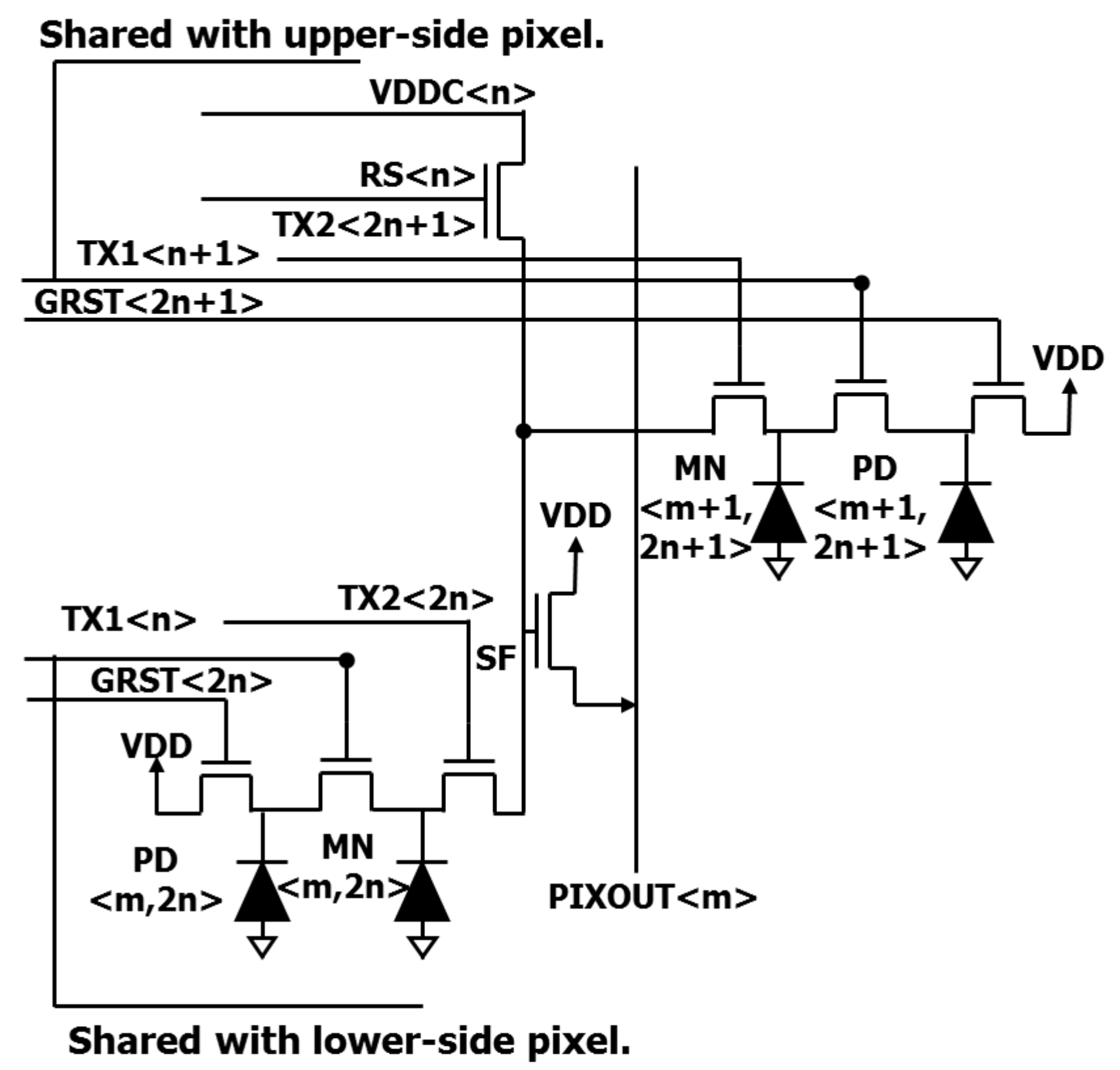
3. Development of 2.5 μm Charge Domain Global Shutter Pixel
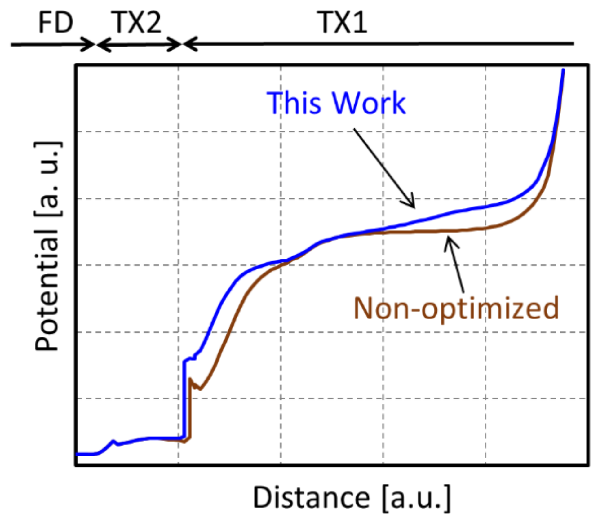
3.1. Design Concept for Charge Domain
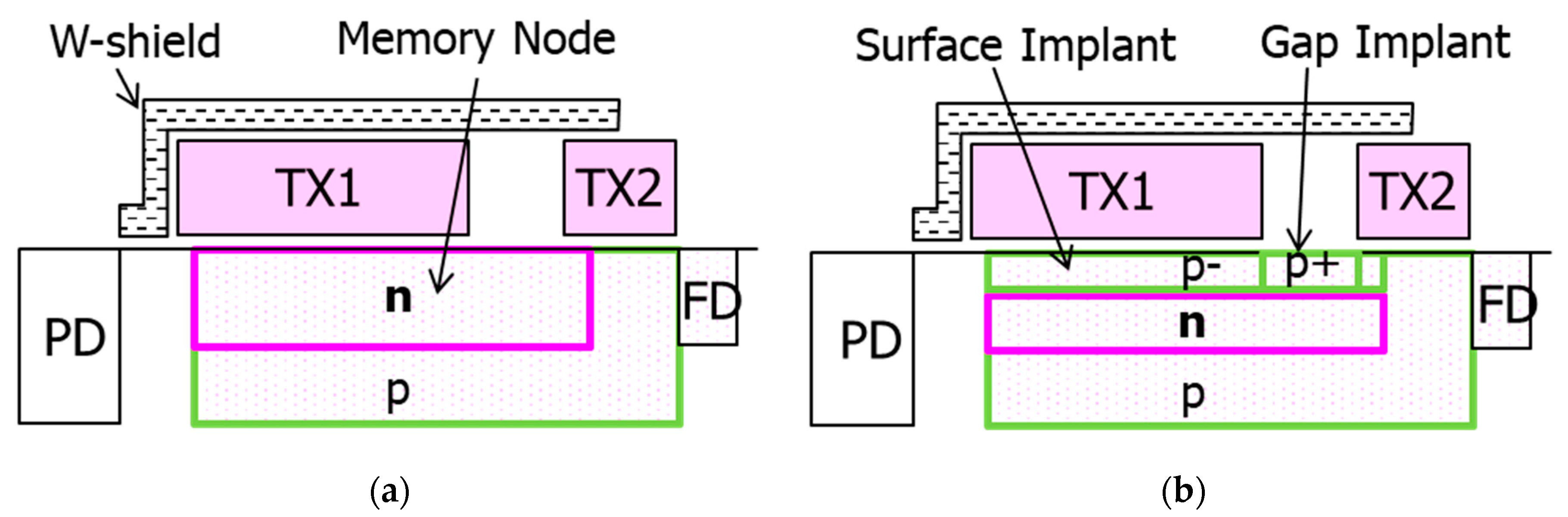
3.2. Memory Node Design
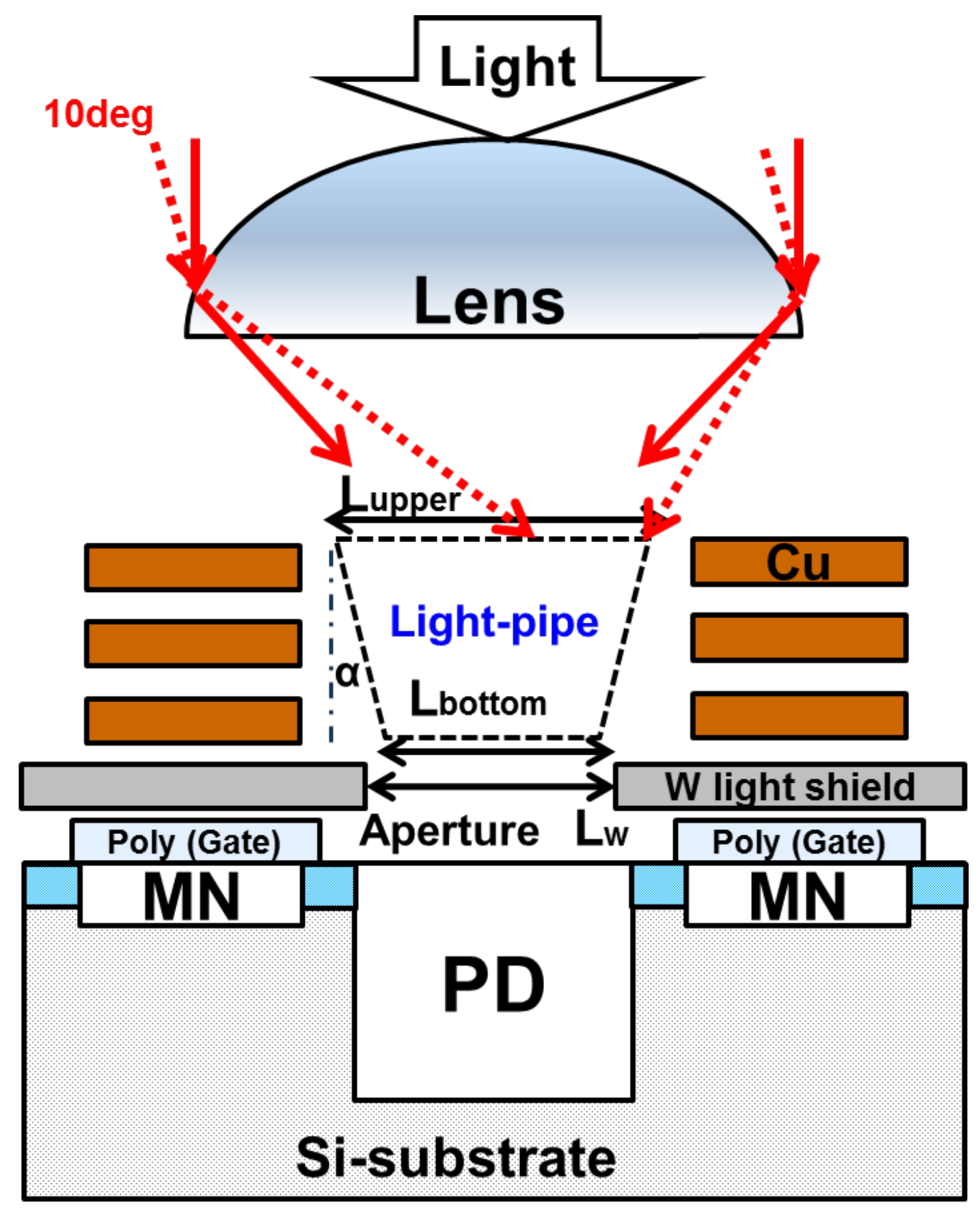
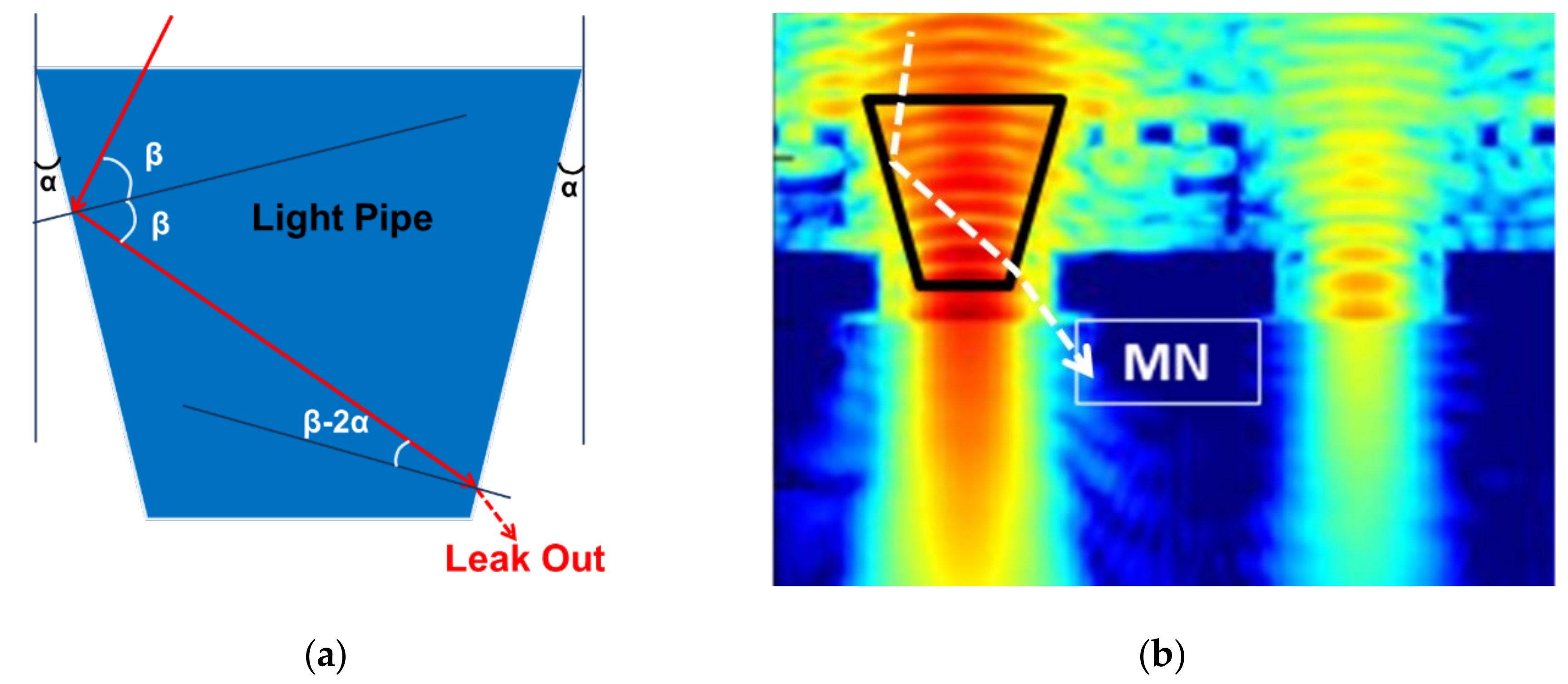
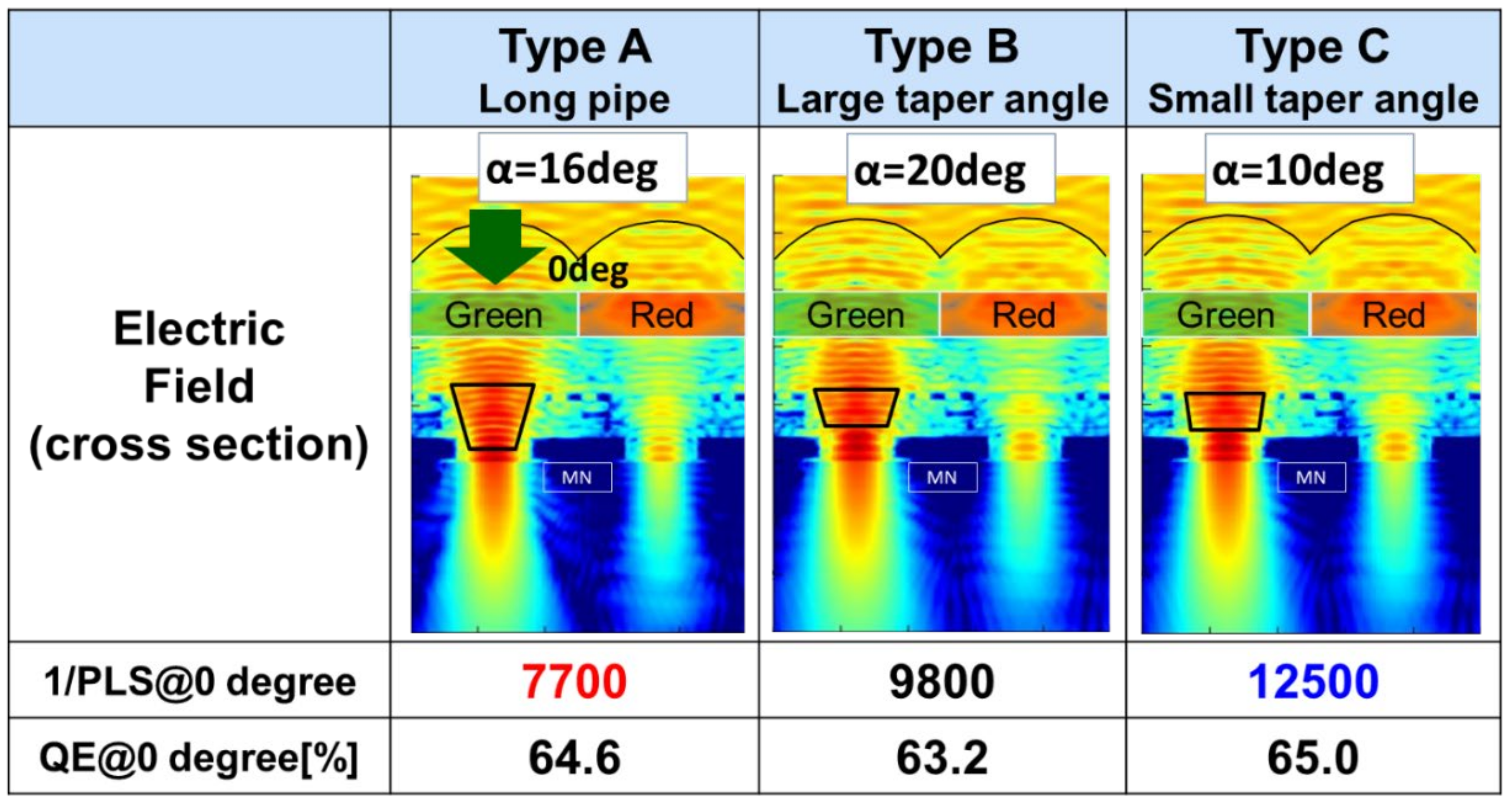
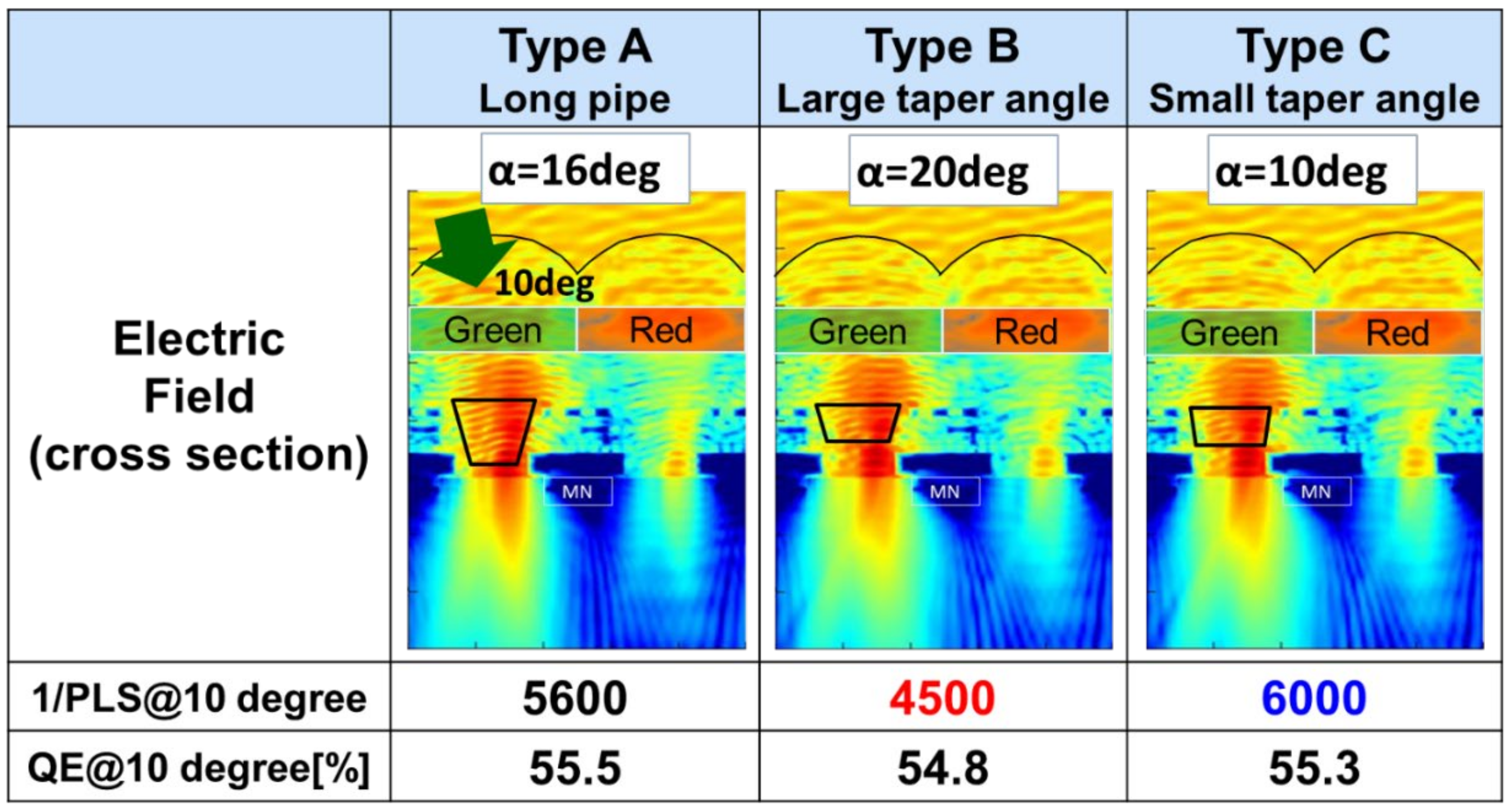
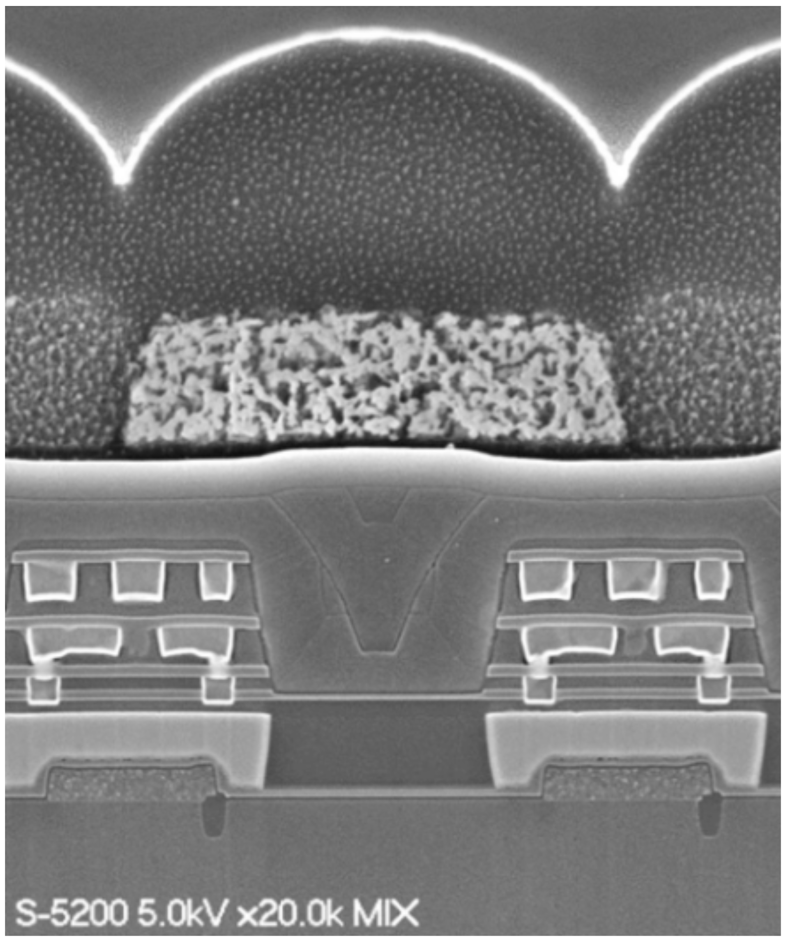
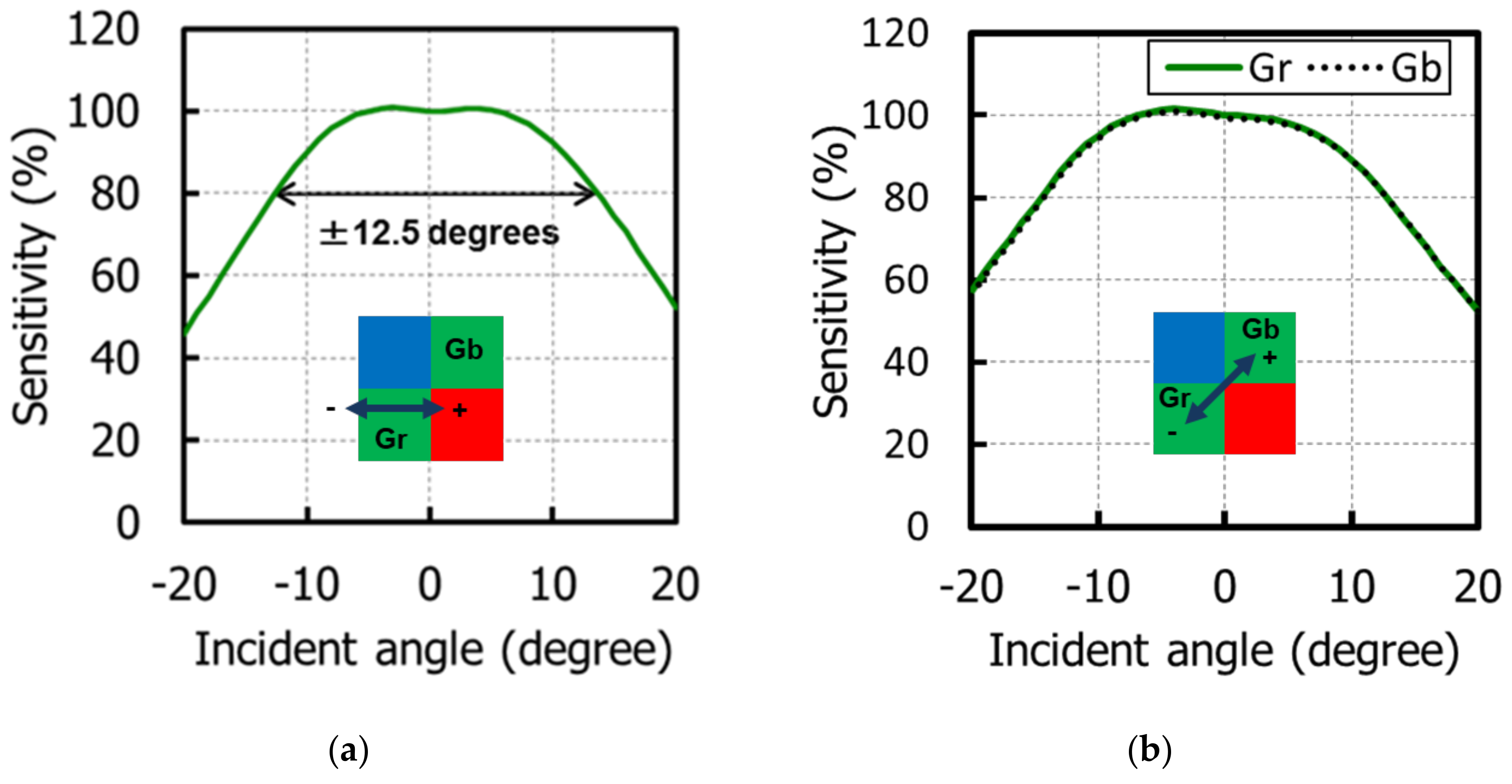
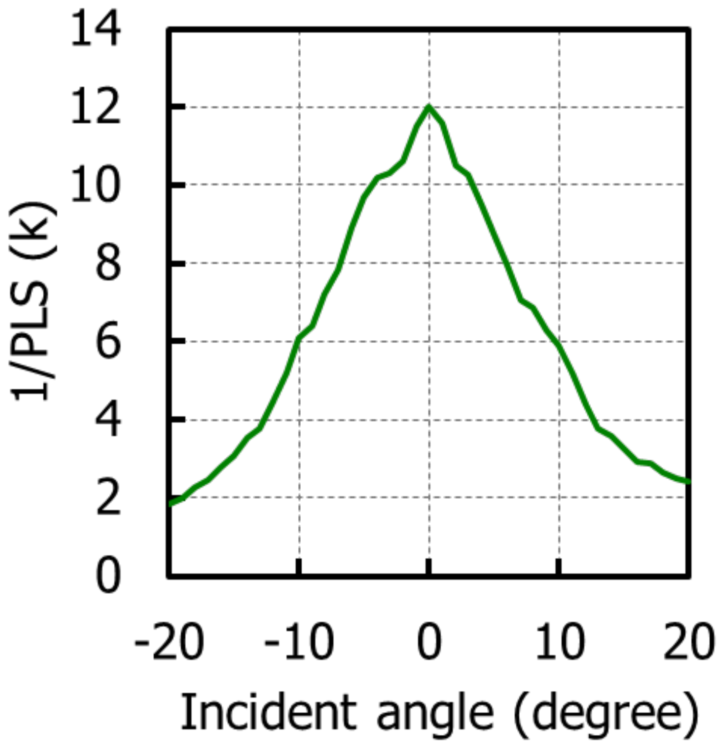
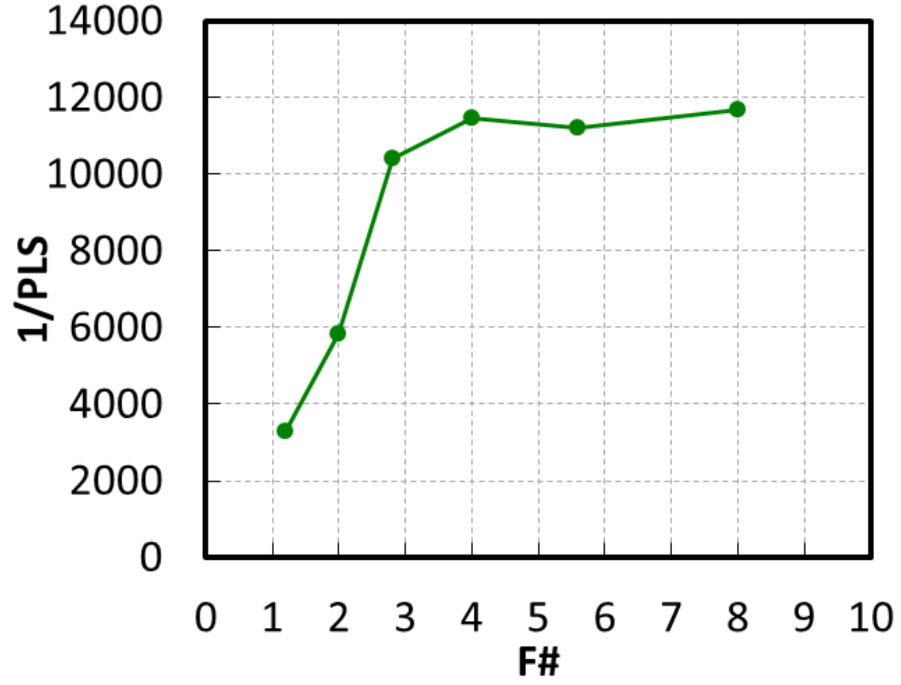
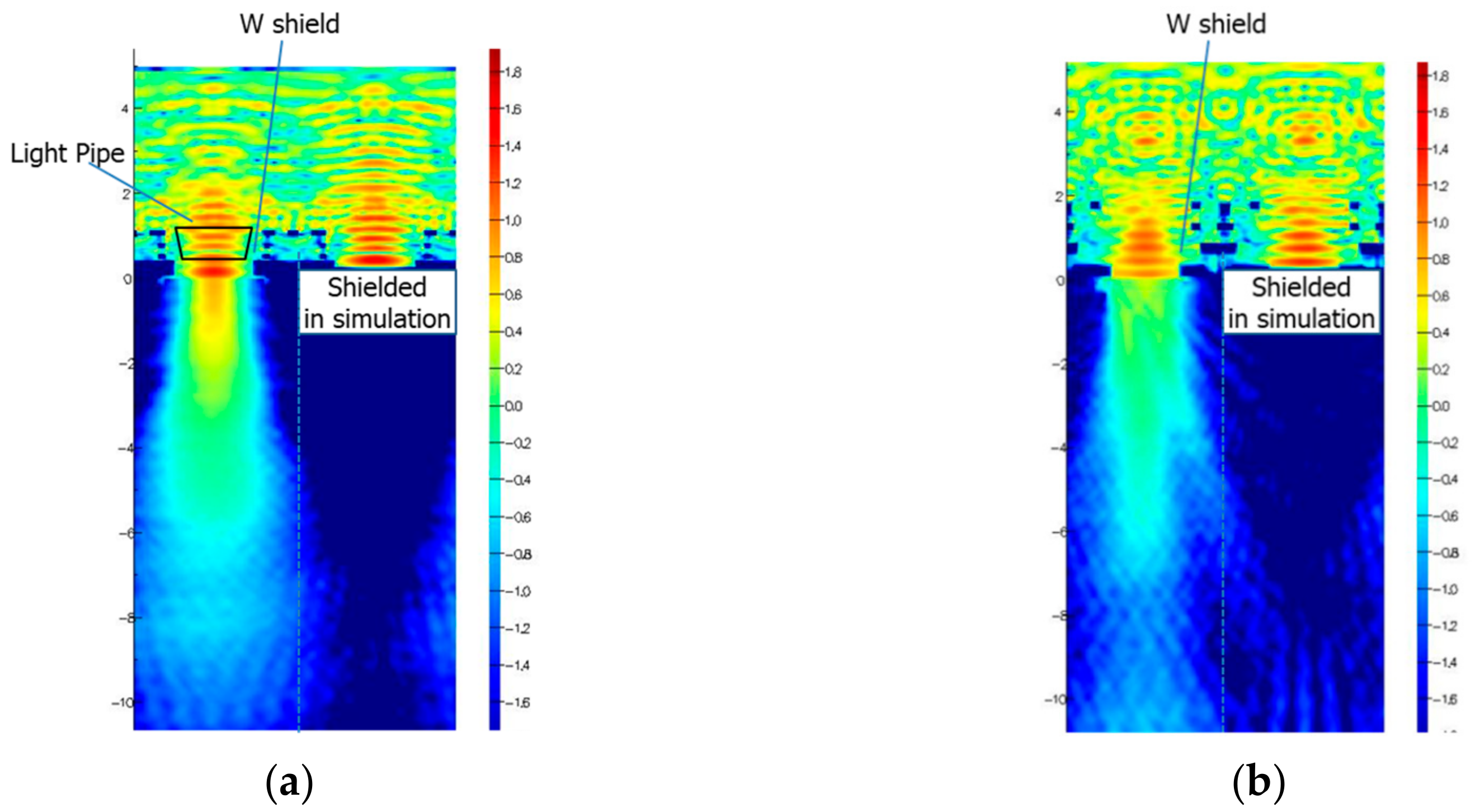
3.3. Optical Design
- (1)
- Type A: Long LP (α was 16 degrees).
- (2)
- Type B: Large taper angle (α was 20 degrees).
- (3)
- Type C: Small taper angle (α was 10 degrees).
3.4. Experimental Result
4. Study of Near-Infrared Enhancement with Light Pipe Technology Using 2.8 μm and 3.2 μm GS Pixels
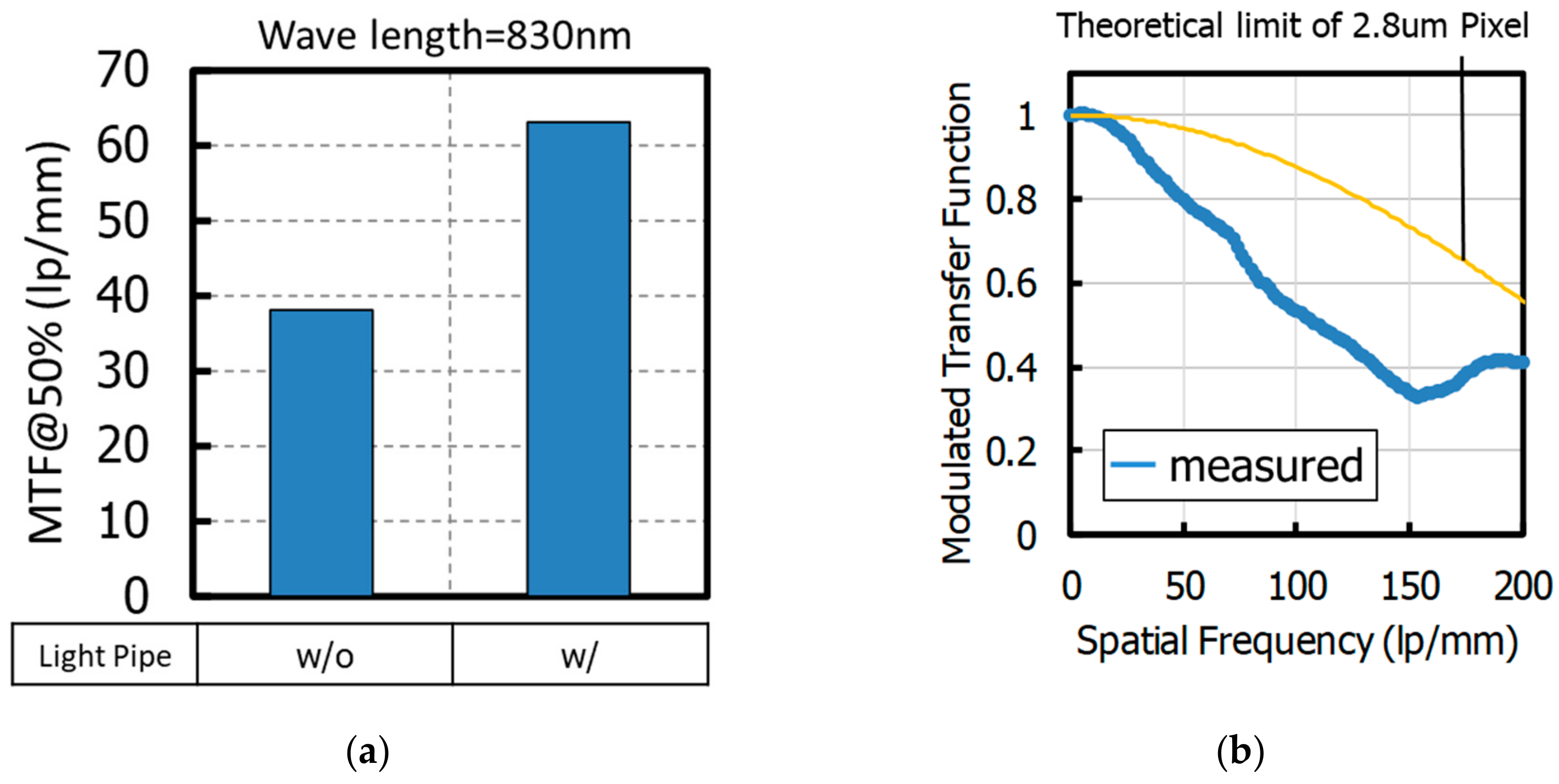
4.1. Effect of Light Pipe on MTF with Near-Infrared Enhancement
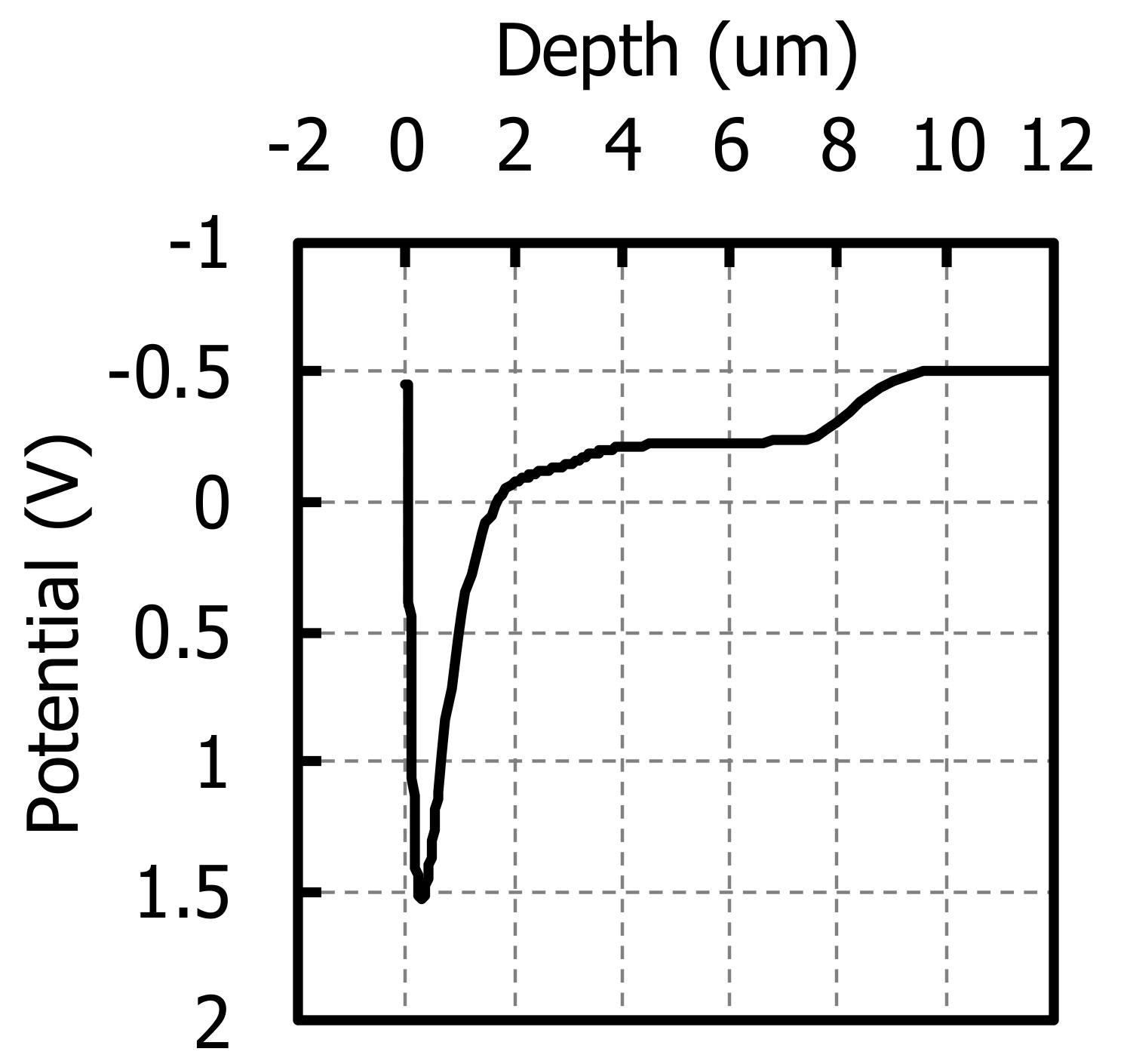
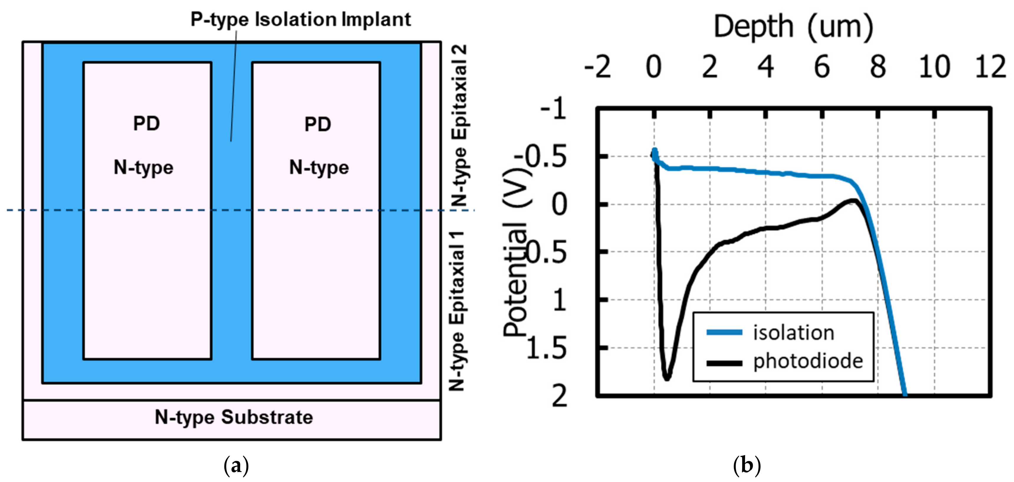
4.2. Further MTF Improvement by Stacked Deep Photodiode Technology
5. Conclusions
Author Contributions
Funding
Acknowledgments
Conflicts of Interest
References
- Yang, G.; Yadid-Pecht, O.; Wrigley, C.; Pain, B. A snap-shot CMOS active pixel imager for low-noise, high-speed imaging. In Proceedings of the International Electron Devices Meeting 1998. Technical Digest (Cat. No. 98CH36217) (IEDM), San Francisco, CA, USA, 6–9 December 1998; pp. 45–48. [Google Scholar]
- Lauxtermann, S.; Lee, A.; Stevens, J.; Joshi, A. Comparison of Global Shutter Pixels for CMOS Image Sensors. In Proceedings of the 2007 International Image Sensor Workshop, Ogunquit, ME, USA, 7–10 June 2007. [Google Scholar]
- Wang, X.; Bogaerts, J.; Vanhorebeek, G.; Ruythoren, K.; Ceulemans, B.; Lepage, G.; Willems, P.; Meynants, G. A 2.2M CMOS Image Sensor for High Speed Machine Vision Applications. In Proceedings of the IS&T/SPIE Electronic Imaging, San Jose, CA, USA, 26 January 2010; Volume 7536. [Google Scholar]
- Meynants, G. Global shutter pixels with correlated double sampling for CMOS image sensors. Adv. Opt. Technol. 2013, 2, 177–187. [Google Scholar]
- Yokoyama, T.; Tsutsui, M.; Nishi, Y.; Mizuno, I.; Dmitry, V.; Lahav, A. High Performance 2.5 um Global Shutter Pixel with New Designed Light-Pipe Structure. In Proceedings of the 2018 International Electron Devices Meeting, San Francisco, CA, USA, 1–5 December 2018. [Google Scholar]
- Velichko, S.; Hynecek, J.J.; Johnson, R.S.; Lenchenkov, V.; Komori, H.; Lee, H.W.; Chen, F.Y. CMOS Global Shutter Charge Storage Pixels with Improved Performance. IEEE Trans. Electron Devices 2015, 63, 106–112. [Google Scholar] [CrossRef]
- Yokoyama, T.; Suzuki, M.; Nishi, Y.; Mizuno, I.; Lahav, A. Design of Double micro lens structure for 2.8 µm Global Shutter Pixel. In Proceedings of the 2017 International Image Sensor Workshop, Hiroshima, Japan, 30 May–2 June 2017. [Google Scholar]
- Tsutsui, M.; Hirata, T.; Tachikawa, K.; Mizuno, I.; Suzuki, M.; Veinger, D.; Birman, A.; Lahav, A. Development of Low Noise Memory Node in a 2.8 μm Global Shutter Pixel with Dual Transfer. In Proceedings of the 2017 International Image Sensor Workshop, Hiroshima, Japan, 30 May–2 June 2017; pp. 28–31. [Google Scholar]
- Yokoyama, T.; Tsutsui, M.; Suzuki, M.; Nishi, Y.; Mizuno, I.; Lahav, A. Development of Low Parasitic Light Sensitivity and Low Dark Current 2.8 μm Global Shutter Pixel. Sensors 2018, 18, 349. [Google Scholar] [CrossRef] [PubMed]
- Mabuchi, K.; Nakamura, N.; Funatsu, E.; Abe, T.; Umeda, T.; Hoshino, T.; Suzuki, R.; Sumi, H. CMOS Image Sensor Using a Floating Diffusion Driving Buried Photodiode. In Proceedings of the 2004 International Solid-State Circuits Conference, San Francisco, CA, USA, 15–19 February 2004. [Google Scholar]
- Yasutomi, K.; Sadanaga, Y.; Takasawa, T.; Itoh, S.; Kawahito, S. Dark Current Characterization of CMOS Global Shutter Pixels Using Pinned Storage Diodes. In Proceedings of the 2011 International Image Sensor Workshop, Hokkaido, Japan, 8–11 June 2011. [Google Scholar]
- Teranishi, N.; Ishihara, Y. Smear reduction in the interline CCD image sensor. IEEE Trans. Electron. Devices 1987, 34, 1052–1056. [Google Scholar] [CrossRef]
- Watanabe, H.; Hirai, J.; Katsuno, M.; Tachikawa, K.; Tsuji, S.; Kataoka, M.; Kawagishi, S.; Kubo, H.; Yano, H.; Suzuki, S.; et al. A 1.4 μm front-side illuminated image sensor with novel light guiding structure consisting of stacked lightpipes. In Proceedings of the IEDM 2011, Washington, DC, USA, 5–7 December 2011. [Google Scholar]
- Velichko, S.; Agranov, G.; Hynecek, J.; Johnson, S.; Komori, H.; Bai, J.; Karasev, I.; Mauritzson, R.; Yi, X.; Lenchenkov, V.; et al. Low Noise High Efficiency 3.75 μm and 2.8 μm Global Shutter CMOS Pixel Arrays. In Proceedings of the 2013 International Image Sensor Workshop, Snowbird Resort, UT, USA, 12–16 June 2013. [Google Scholar]
- Wang, C.; Ma, Y.; Guo, Z.; Li, G.; Xin, H.; Yin, Y.; Liu, Y.; Li, Q.; Zhou, J.; Bogaerts, X. High speed 25M global shutter image sensor with 2.5um pixel. In Proceedings of the 2019 International Image Sensor Workshop, Snowbird, UT, USA, 23–27 June 2019. [Google Scholar]
- Sekine, H.; Kobayashi, M.; Onuki, Y.; Kawabata, K.; Tsuboi, T.; Matsuno, Y.; Takahashi, H.; Inoue, S.; Ichikawa, T. Development of Gentle Slope Light Guide Structure in a 3.4 μm Pixel Pitch Global Shutter CMOS Image Sensor with Multiple Accumulation Shutter Technology. Sensors 2017, 17, 2860. [Google Scholar] [CrossRef] [PubMed]
- Tournier, A.; Roy, F.; Cazaux, Y.; Lalanne, F.; Malinge, P.; Mcdonald, M.; Monnot, G.; Roux, N. A HDR 98 dB 3.2 μm Charge Domain Global Shutter CMOS Image Sensor. In Proceedings of the 2018 International Electron Devices Meeting, San Francisco, CA, USA, 1–5 December 2018. [Google Scholar]
- Lahav, A.; Birman, A.; Veinger, D.; Fenigstein, A.; Zhang, D.; Blerkom, D. IR Enhanced Global Shutter Pixel for High Speed Applications. In Proceedings of the 2013 International Image Sensor Workshop, Snowbird, UT, USA, 12–16 June 2013. [Google Scholar]
- Kishino, K.; Unlu, M.S.; Chyi, J.-I.; Reed, J.; Arsenault, L.; Morkoc, H. Resonant cavity-enhanced (RCE) photodetectors. IEEE J. Quantum Electron. 1991, 27, 2025–2034. [Google Scholar] [CrossRef]
- Yokogawa, S.; Oshiyama, I.; Ikeda, H.; Ebiko, Y.; Hirano, T.; Saito, S.; Oinoue, T.; Hagimoto, T.; Iwamoto, H. IR sensitivity enhancement of CMOS Image Sensor with diffractive light trapping pixels. Sci. Rep. 2017, 7, 3832. [Google Scholar] [CrossRef] [PubMed]
- Takahashi, H.; Tanaka, H.; Oda, M.; Ando, M.; Niisoe, N.; Kawai, S.; Asano, T.; Sudo, M.; Yoshita, M.; Yamada, T. Novel Pixel Structure with Stacked Deep Photodiode to Achieve High NIR Sensitivity and High MTF. In Proceedings of the VLSI Technology, Honolulu, HI, USA, 13–16 June 2016. [Google Scholar]


| Photo Diode (PD) | Memory Node (MN) | |
|---|---|---|
| Light Sensitivity | Lager-is-better (QE) | Smaller-is-better (PLS) |
| Angular Response of Sensitivity | Lager-is-better | Smaller-is-better |
| Full Well Capacity | Lager-is-better | Larger than PD |
| DC, DSNU | Smaller-is-better | |
| Lag | Smaller-is-better | |
| Pixel Performance | Unit | 2.5um | |
|---|---|---|---|
| Conversion Gain @SF out | uV/e− | 100 | |
| Linear FWC @PD (max SNR) | e− | 6300 | |
| Saturated FWC @ MN | e− | >9000 | |
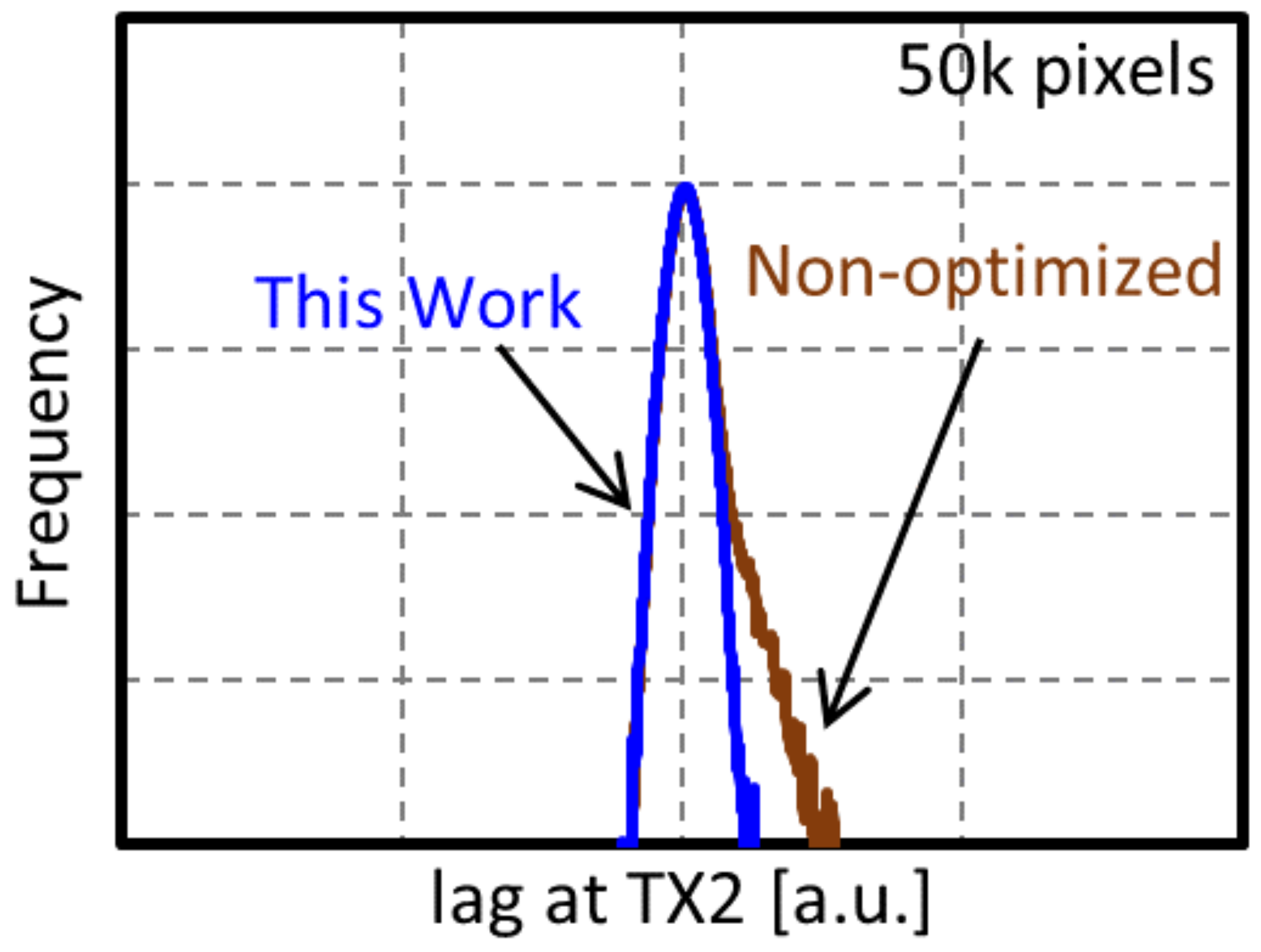
| Image Lag @ TX2 | e− | 0 | |
| Image Lag @ TX1 | e− | 0 | |
| Image Lag @ GRST | e− | 0 | |
| Temporal Noise | e− rms | 1.5 | |
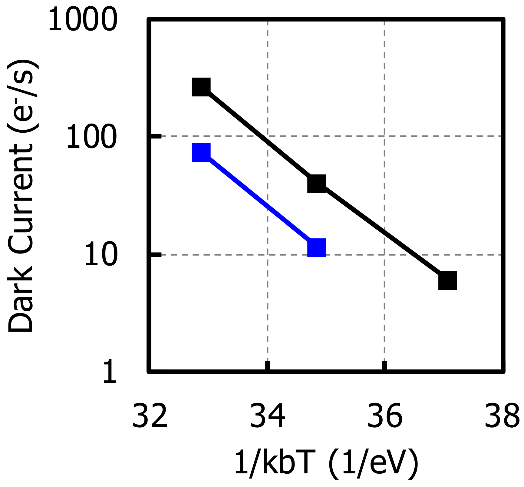
| Dark Current | @ PD (60C) | e−/s | 43 |
| Standard Deviation | e−/s | 28 | |
| Dark Current | @ MN (60C) | e−/s | 13 |
| Standard Deviation | e−/s | 24 | |
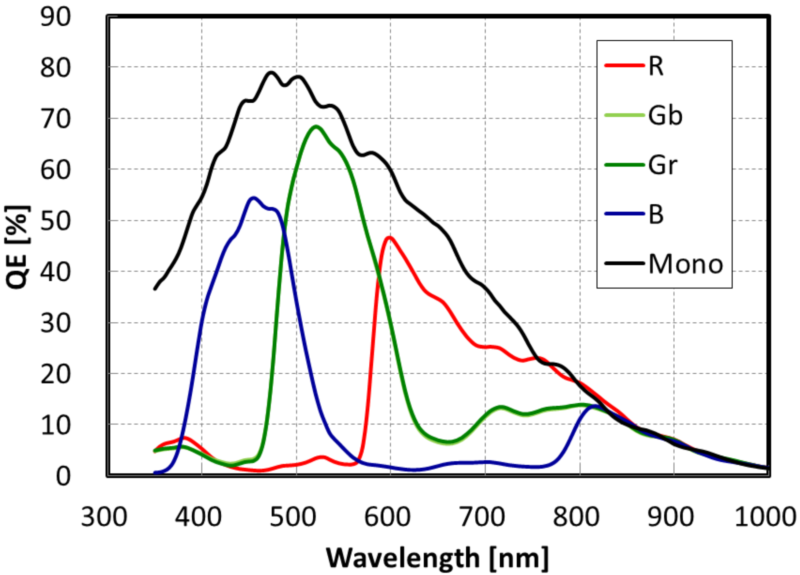
| QE @ Green (λ = 530 nm) | % | 68 | |
| AR of Sensitivity | degree | 12.5 | |
| 1/PLS @ F2.8 | - | 10,400 | |
| Ea (eV) | Doubling Factor (°C) | |
|---|---|---|
| MN | 0.98 | 5.5 |
| PD | 0.95 | 5.8 |
| Unit | This Work | [14] IISW2013 | [16] IISW2017 | [17] IEDM2018 | |
|---|---|---|---|---|---|
| Pixel Pitch | μm | 2.5 | 2.8 | 3.4 | 3.2 |
| Linear FWC (Per pixel area) | e− (e−/μm2) | 6300 (1008) | 6000 (765) | 6100 (528) | 7100 (693) |
| Dark Current at MN | e−/s | 13 | 60 | - | 5 |
| Peak QE (mono) | % | 78 | 70 | 62 | 72.9 |
| Sensitivity | e−/lx s | 30,800 | - | 28,000 | - |
| 1/PLS (mono) | - | 8100 | 2200 | 28,000 | 3333 @λ = 505 nm |
| Pixel Performance | Unit | 3.2 um | |
|---|---|---|---|
| Conversion Gain @SF out | uV/e− | 80 | |
| Linear FWC @PD (max SNR) | e− | 10,200 | |
| Saturated FWC @ MN | e− | >14,000 | |
| Image Lag @ TX2 | e− | 0 | |
| Image Lag @ TX1 | e− | 0 | |
| Image Lag @ GRST | e− | 0 | |
| Temporal Noise | e− rms | 1.6 | |
| Dark Current | @ PD (60C) | e−/s | 66 |
| Standard deviation | e−/s | 54 | |
| Dark Current | @ MN (60C) | e−/s | 25 |
| Standard deviation | e−/s | 12 | |
| QE @ λ = 940 nm | % | 9 | |
| AR of Sensitivity | degree | 16 | |
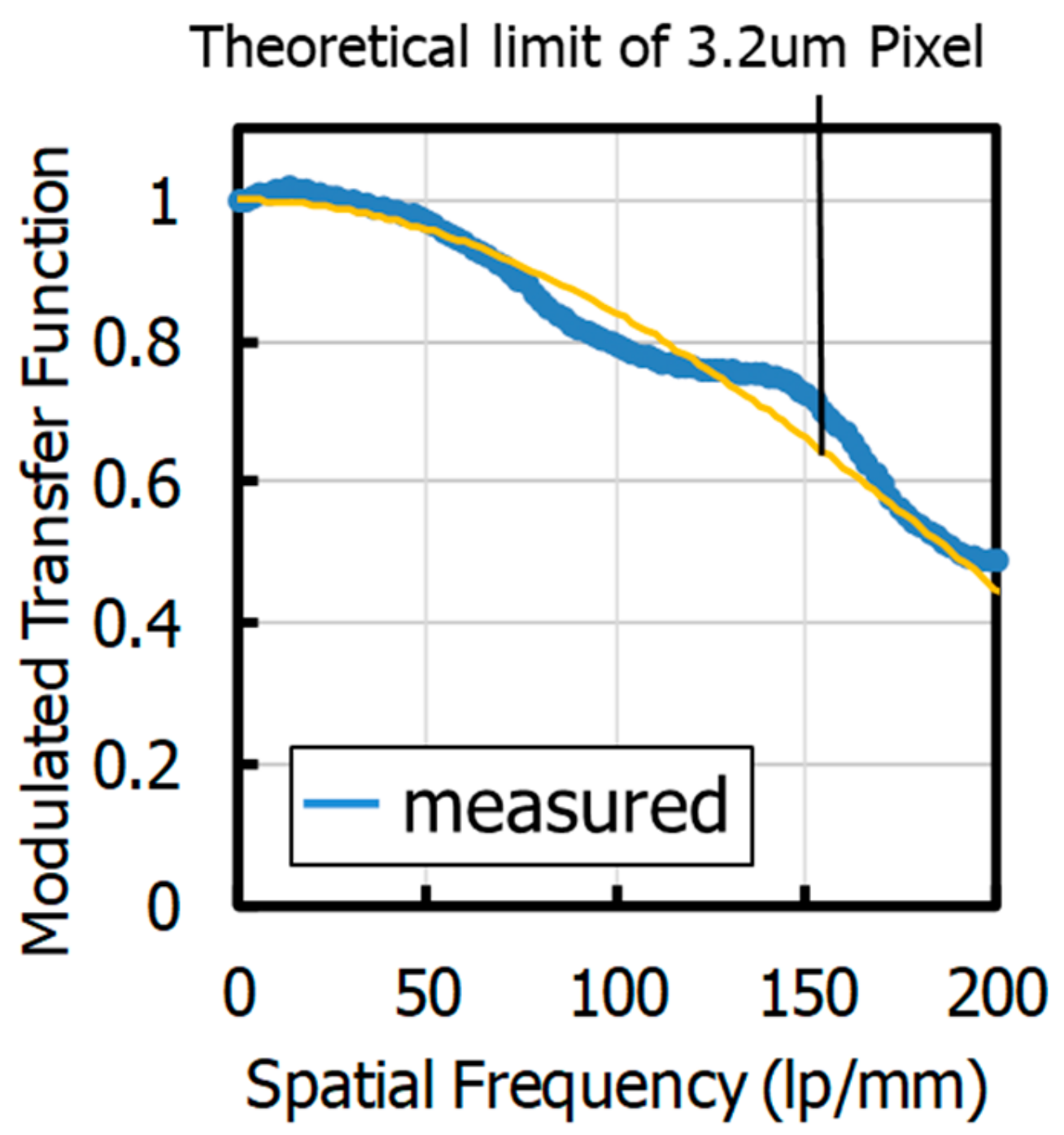
| MTF @50%, λ = 940 nm | lp/mm | 156 (theoretical limit) | |
© 2020 by the authors. Licensee MDPI, Basel, Switzerland. This article is an open access article distributed under the terms and conditions of the Creative Commons Attribution (CC BY) license (http://creativecommons.org/licenses/by/4.0/).
Share and Cite
Mizuno, I.; Tsutsui, M.; Yokoyama, T.; Hirata, T.; Nishi, Y.; Veinger, D.; Birman, A.; Lahav, A. A High-Performance 2.5 μm Charge Domain Global Shutter Pixel and Near Infrared Enhancement with Light Pipe Technology. Sensors 2020, 20, 307. https://doi.org/10.3390/s20010307
Mizuno I, Tsutsui M, Yokoyama T, Hirata T, Nishi Y, Veinger D, Birman A, Lahav A. A High-Performance 2.5 μm Charge Domain Global Shutter Pixel and Near Infrared Enhancement with Light Pipe Technology. Sensors. 2020; 20(1):307. https://doi.org/10.3390/s20010307
Chicago/Turabian StyleMizuno, Ikuo, Masafumi Tsutsui, Toshifumi Yokoyama, Tatsuya Hirata, Yoshiaki Nishi, Dmitry Veinger, Adi Birman, and Assaf Lahav. 2020. "A High-Performance 2.5 μm Charge Domain Global Shutter Pixel and Near Infrared Enhancement with Light Pipe Technology" Sensors 20, no. 1: 307. https://doi.org/10.3390/s20010307
APA StyleMizuno, I., Tsutsui, M., Yokoyama, T., Hirata, T., Nishi, Y., Veinger, D., Birman, A., & Lahav, A. (2020). A High-Performance 2.5 μm Charge Domain Global Shutter Pixel and Near Infrared Enhancement with Light Pipe Technology. Sensors, 20(1), 307. https://doi.org/10.3390/s20010307