Enhancing Sensor Network Security with Improved Internal Hardware Design


Abstract
:
1. Introduction
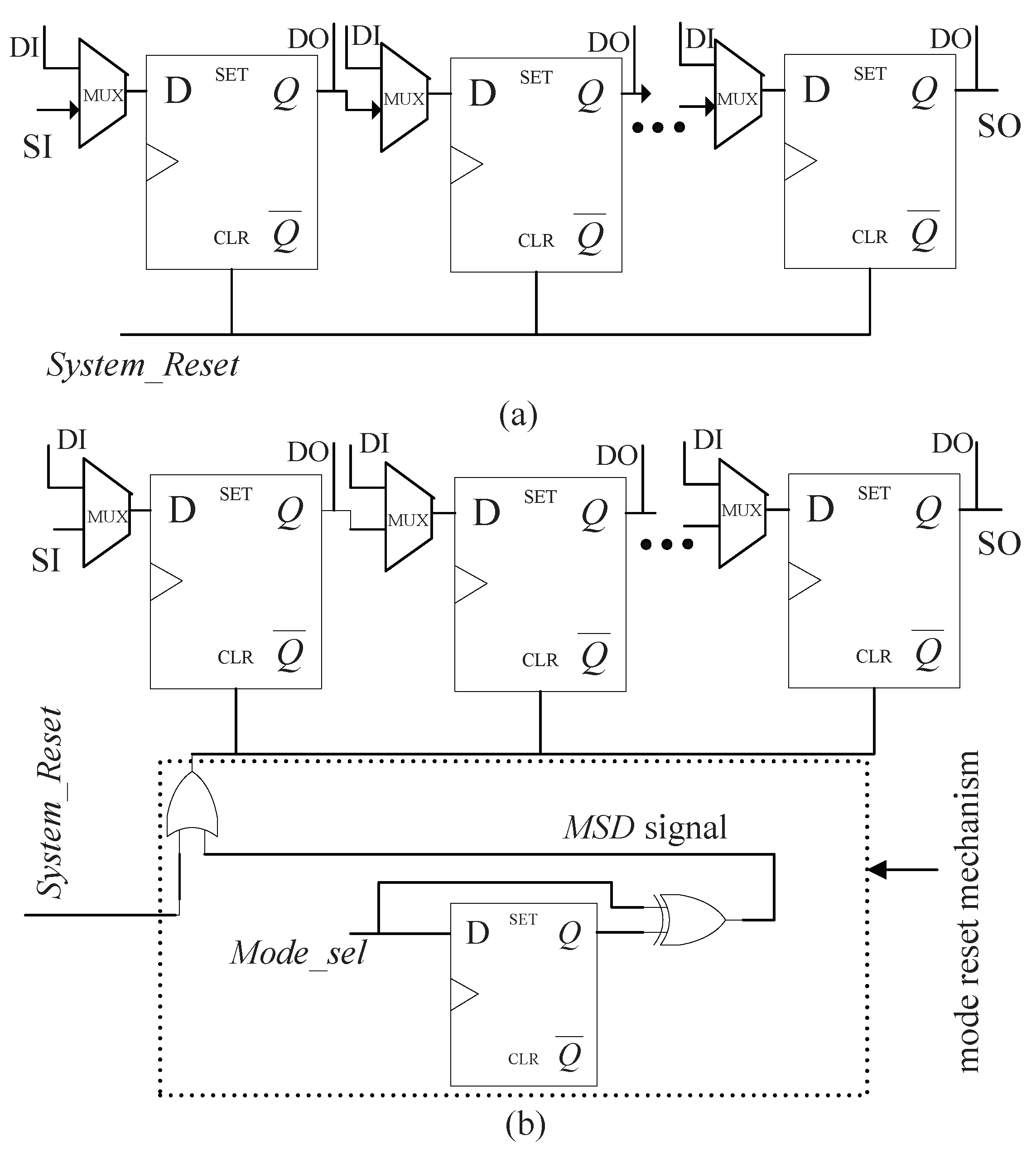
- Protection of mode switching: By introducing the test controller, the values of the scan flip-flops will be reset once switch from functional mode to test mode is requested [31,32,33]. However, this countermeasure is solely applicable for mode-switching attacks and powerless to test-mode-only attacks.
- Blocking of encryption key: In reference [22], secure scan architecture including MKRs (Mirror Key Registers) is utilized. it exploits two operation modes: insecure and secure modes. In insecure mode, the cipher key is prohibited from entering MKRs, but test vectors can be loaded into scan chains and test responses can also be captured and scanned out. In secure mode, the cryptographic circuit can work properly but can not return to insecure mode to conduct test and debug operation. For this type of countermeasure, it may be impossible to gain encryption data corresponding to a known plaintext discretionarily. However, the clunky test control architecture brings negative impact on IP design.
- Improvment of scan architecture: In reference [34], a secure scan architecture called differential scan path is proposed to improve the chip security. In the technique, the state of the scan path is divided into two segments. In test mode, only subtraction of the segment states can be observed at the scan-out ports. Deriving the intermediate state from the difference results needs much guesswork. The guessing probability decreases exponentially when the length of the scan path increases.
- Obfuscation of scan-out data: This countermeasure inserts obfuscation logics such as dummy flip-flops, exclusive-or (XOR) gates, inverters, lock and key logic, into the scan chains to change scan-out data randomly [35,36,37,38,39,40]. If the scan-out data is obfuscated, an attacker may be misguided to deduce the inaccurate key or be unable to calculate the cipher key. The scan-out encryption result is obfuscated by dynamically altering the join order of the sub-chains in [35,36]. Nevertheless, the calculating signature attacks can still be implemented even if attackers don’t know the scan architecture or scan flip-flop order [41,42]. A key and lock method was introduced in [37] to thwart signature attacks. Several scan flip-flops are selected to make their shift-enabling signal controlled by the values of an additional shift register (i.e., test key). In test phase, the reshuffled scan cells controlled by inaccurate bits of test key will remain in functional mode instead of test mode. Obfuscation of scan data is achieved as the scan-out data is actually not the test response captured in scan chains. To resist test-mode-only signature attack, an improved technique refereed as dynamic obfuscation of scan data was also presented in [37]. The inaccurate test key is cyclically shifted in test phase, and thus the scan-out data will be rather more erratic. However, this modified scan design involves some hardware overhead and cannot apply to delay test based on Launch-off-Capture (LOC).
- Scan Chain Encryption: The secure technique proposed in [43] uses the secret-key management policy to encrypt the scan chain content during test. Only the test engineers who have the key can deliver desired data into scan chains and shift out intermediate states from scan chains. The secure scheme proposed in [44] encrypts the data written to or read from the scan chains by using an on-chip lightweight block cipher. Such techniques require a crypto core insertion in the scan chains, which increases the complexity of scan design.
2. Preliminaries
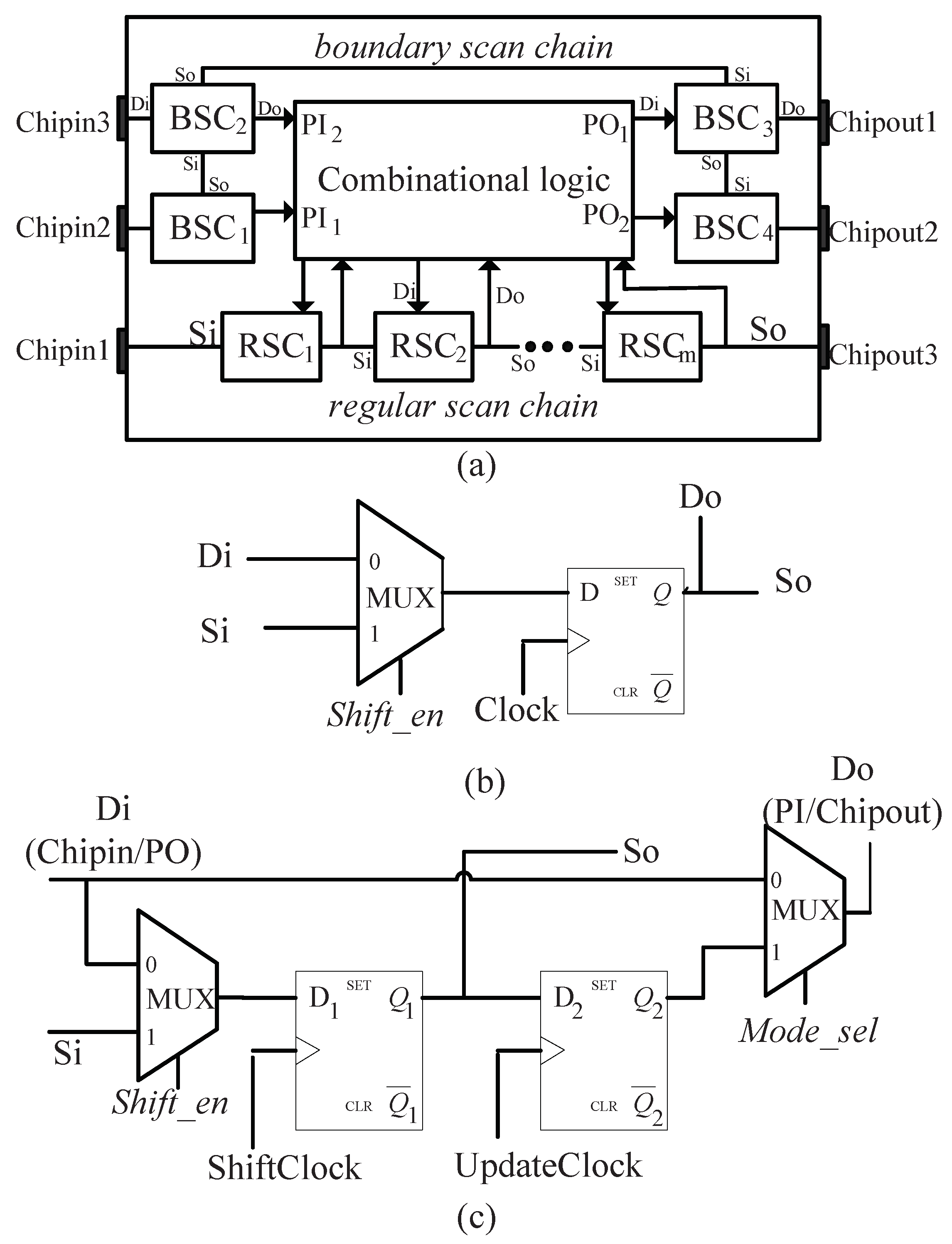
2.1. Scan Design
- When the chip runs in the functional mode, = 0 and = 0. The RSCs are driven by combinational logic, and BSCs are transparent (data passes from Di directly to Do).
- When the chip runs in test mode, = 1 and there are three operation phases: Shift, Update and Capture.
- -
- In the Shift phase, is assigned to ‘1’ and clock pulses are applied to ShiftClock of each BSC and clock input of each RSC such that test patterns can be scanned in from Si of (boundary and regular) scan chains and test responses can be scanned out through So of scan chains.
- -
- In the Update phase, which targets only BSCs, the test data stored in D1 (termed as the capture flip-flop) are propagated to D2 (termed as the update flip-flop) by giving a clock pulse to Updateclock of each BSC. At this time, the state of D2 determines the Do of BSC.
- -
- In the Capture phase, is set to ‘0’, one clock pulse is applied to ShiftClock of each BSC and clock input of each RSC, and the test response at Di will be captured into RSC or the D1 of BSC.
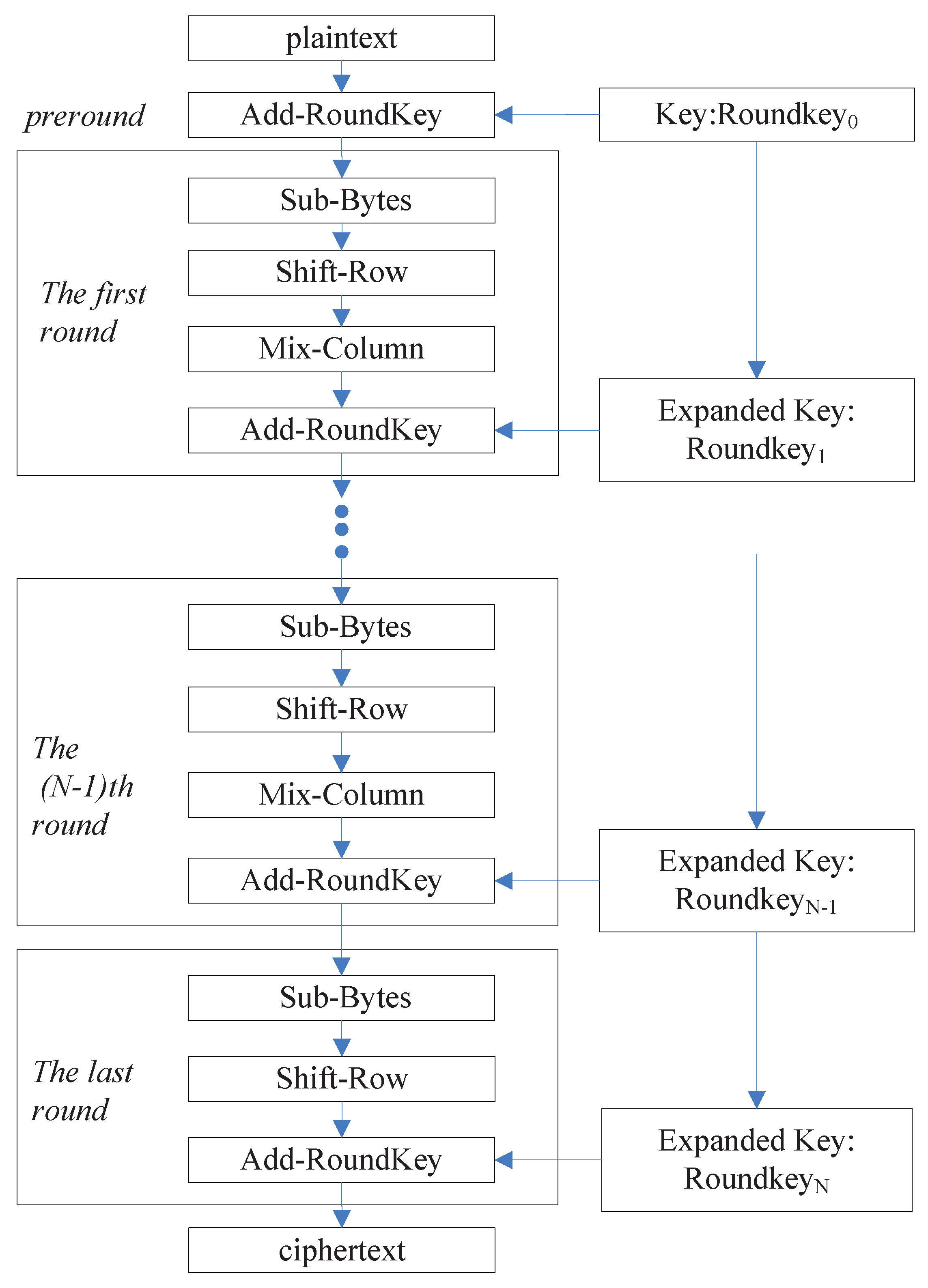
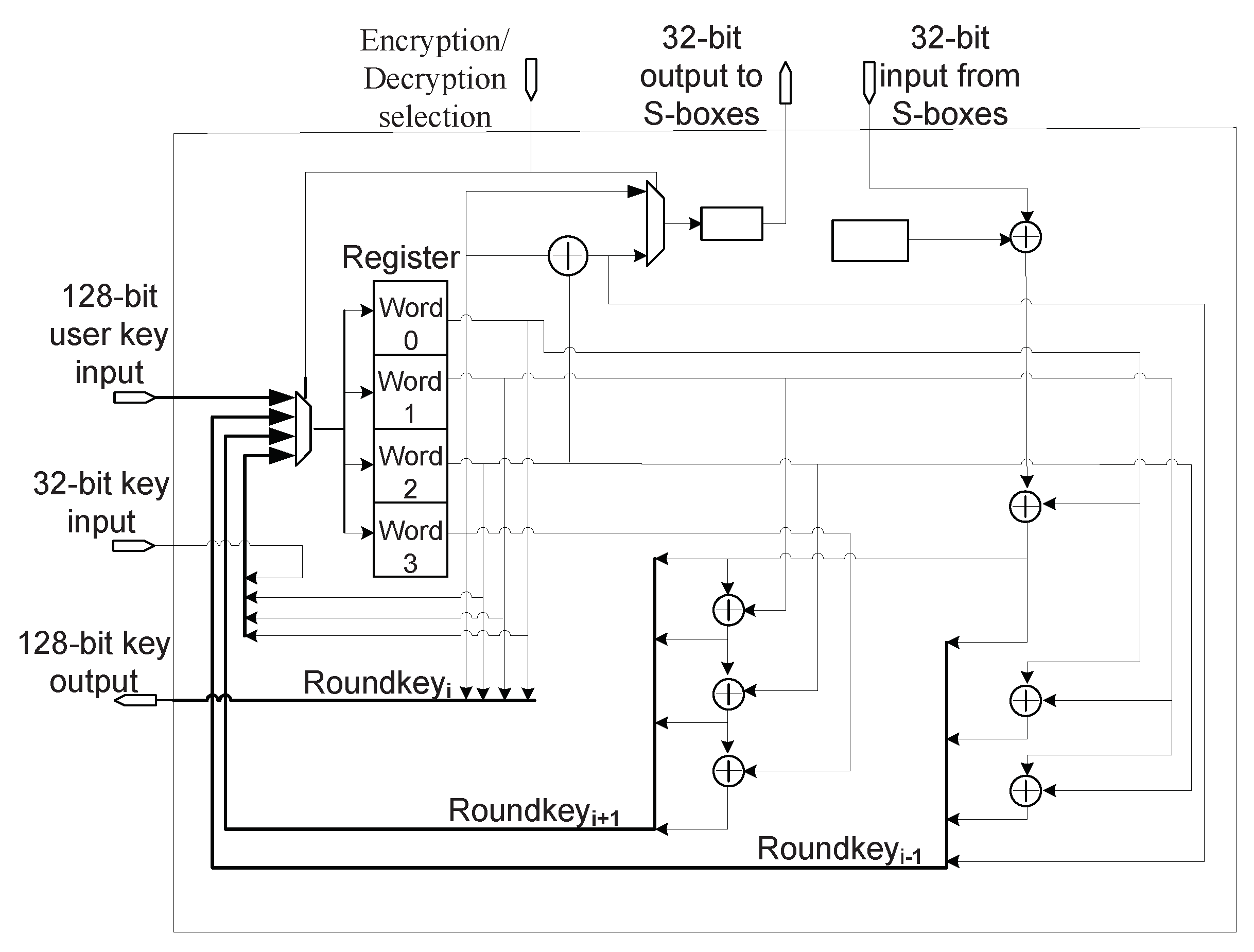
2.2. AES and Its Hardware Implementation
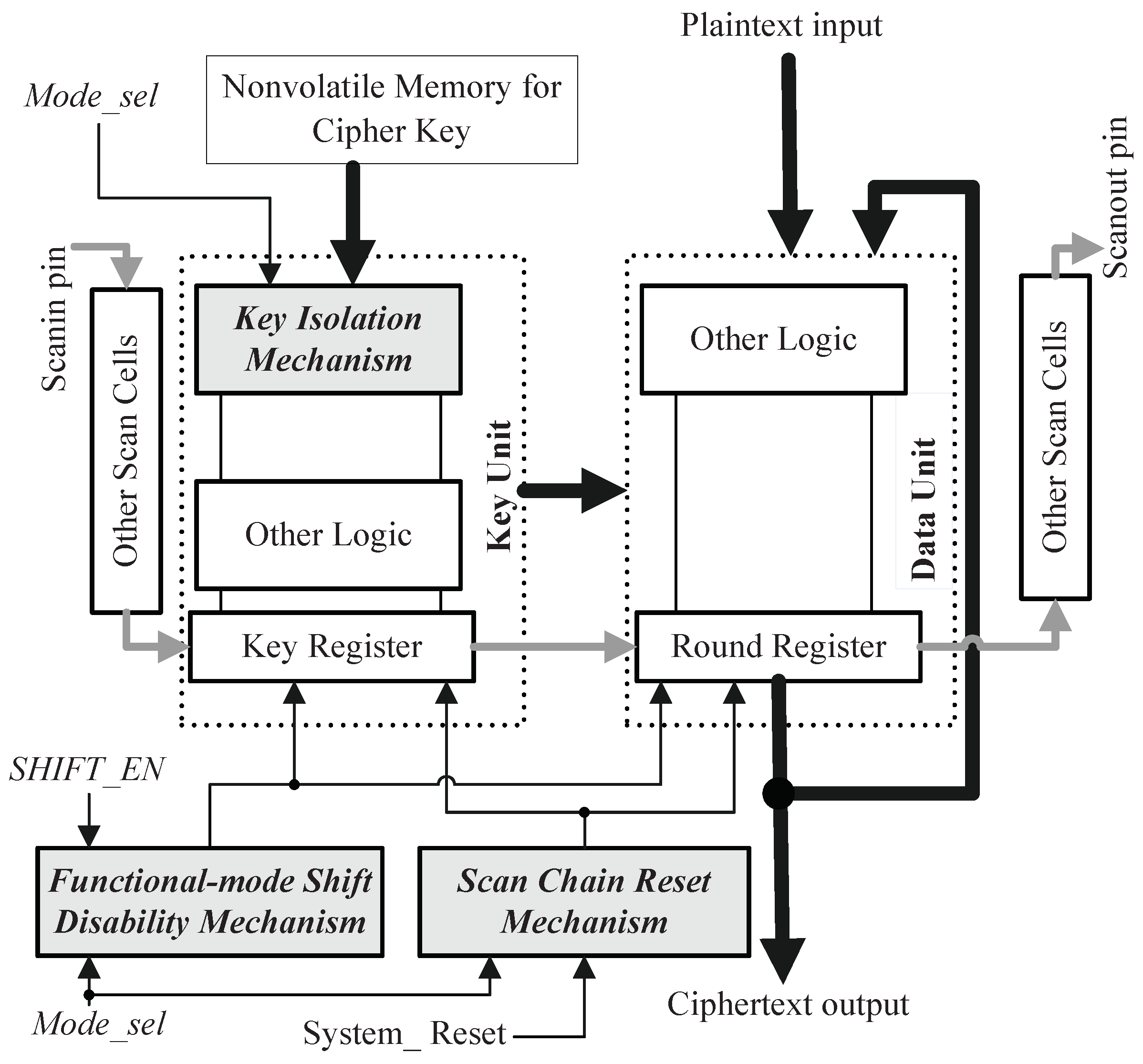
3. Proposed Secure Scan Test Scheme
- Functional-mode attack. This attack consists of 2 steps. In the first step, a pre-computed plaintext is delivered to the primary inputs when the crypto chip works in functional mode ( = 0 & = 0) for only one round of AES algorithm. The state of the one round operation is stored in the scan chains. In the second step the crypto chip remains in functional mode but shift-enabling signal is set to ‘1’ ( = 0 & = 1) and the encryption result in scan chains is shifted out for analysis. Such 2-step operation is duplicated for different plaintexts until the cipher key are successfully deduced.
- Mode-switching attack. This attack also consists of 2 steps. In the first step, a pre-computed plaintext is delivered to the primary inputs when the crypto chip works in functional mode ( = 0 & = 0) for only one round of AES algorithm. The first step is similar with that of functional-mode attack. The only difference is that, in the second step the crypto circuit is converted into shift phase of test mode ( = 1 & = 1) and then the encryption result in scan chains is shifted out.
- Test-mode-only attack. The crypto chip runs in test mode ( = 1) throughout this attack. This attack consists of 4 steps. In the first step, the plaintext is scanned into boundary scan cells corresponding to primary inputs under shift phase ( = 1). In the second step, the plaintext is delivered to the primary inputs from boundary scan cells in update phase. Then the chip runs under capture phase ( = 0) to store the result of the round operation in the scan chains. In the last step, the crypto chip enters again shift phase ( = 1) and the round result in scan chains is shifted out while the next plaintext is shift into. The four steps are also repeated for different plaintexts until the cipher key is successfully deduced.
- The testability and debuggability of crypto core should be guaranteed by using scan-based DFT.
- The intermediate encrypted result saved in scan chains must not be accessed to crack the cipher key. In other words, the values that could be shifted out of scan chains must be unrelated to the cipher key or be obfuscated.
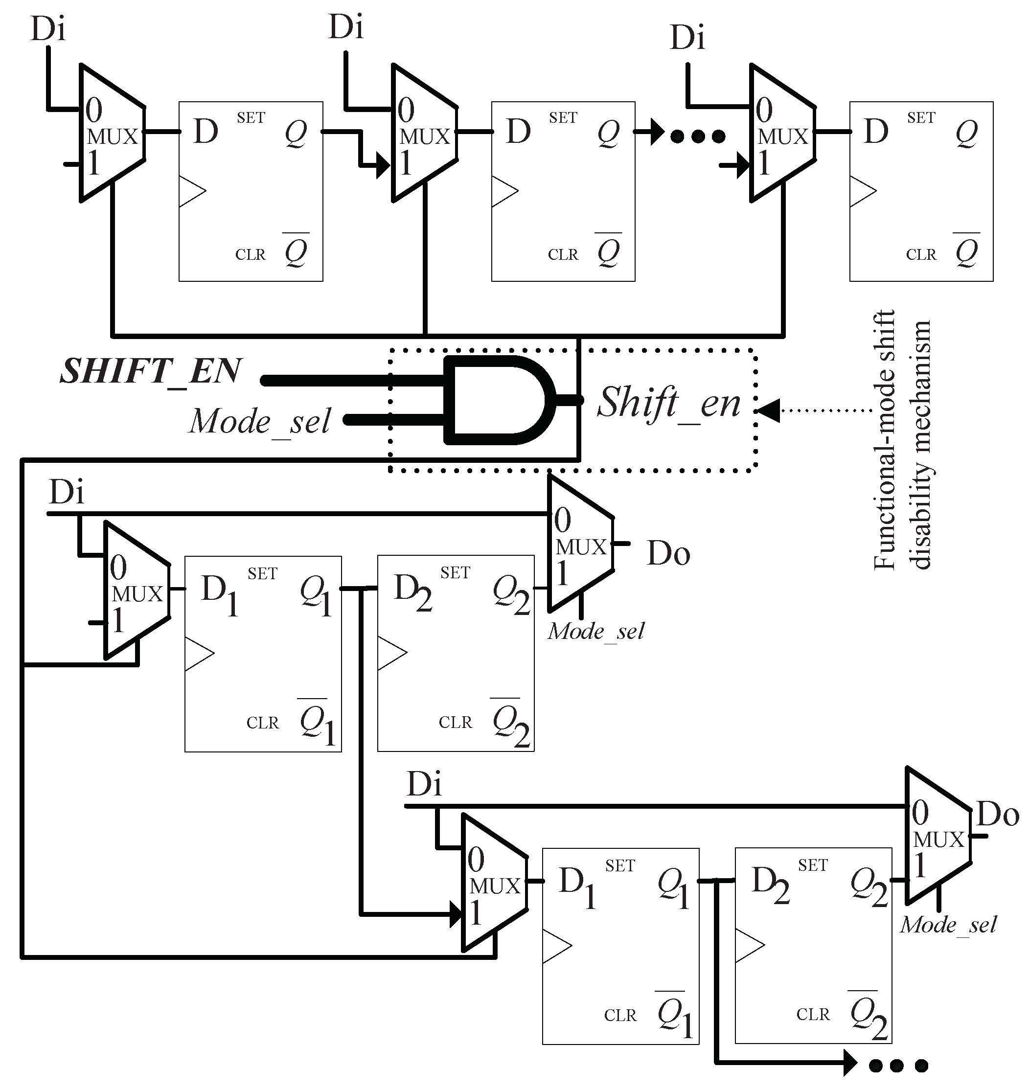
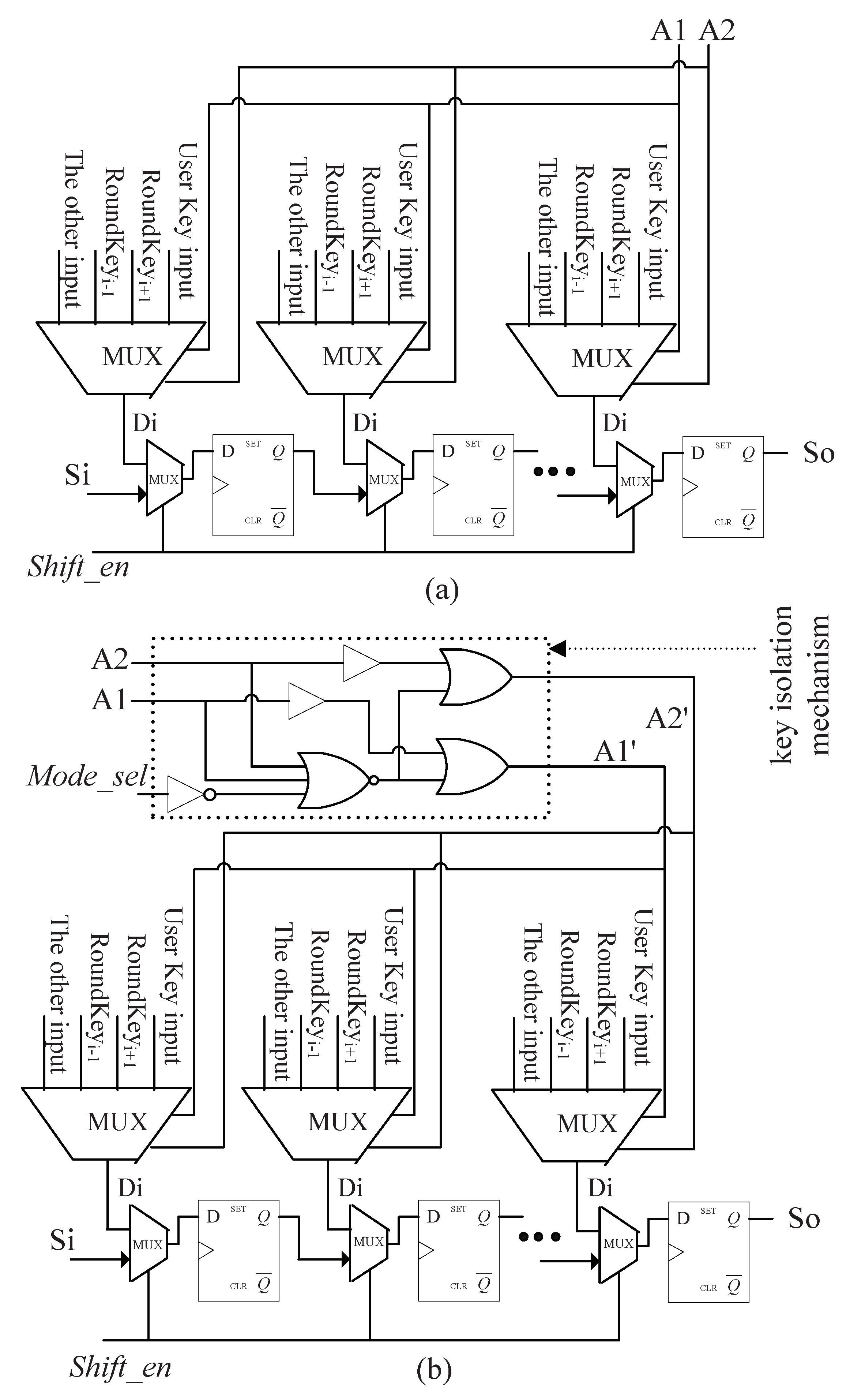
3.1. Proposed Secure Scan Architecture
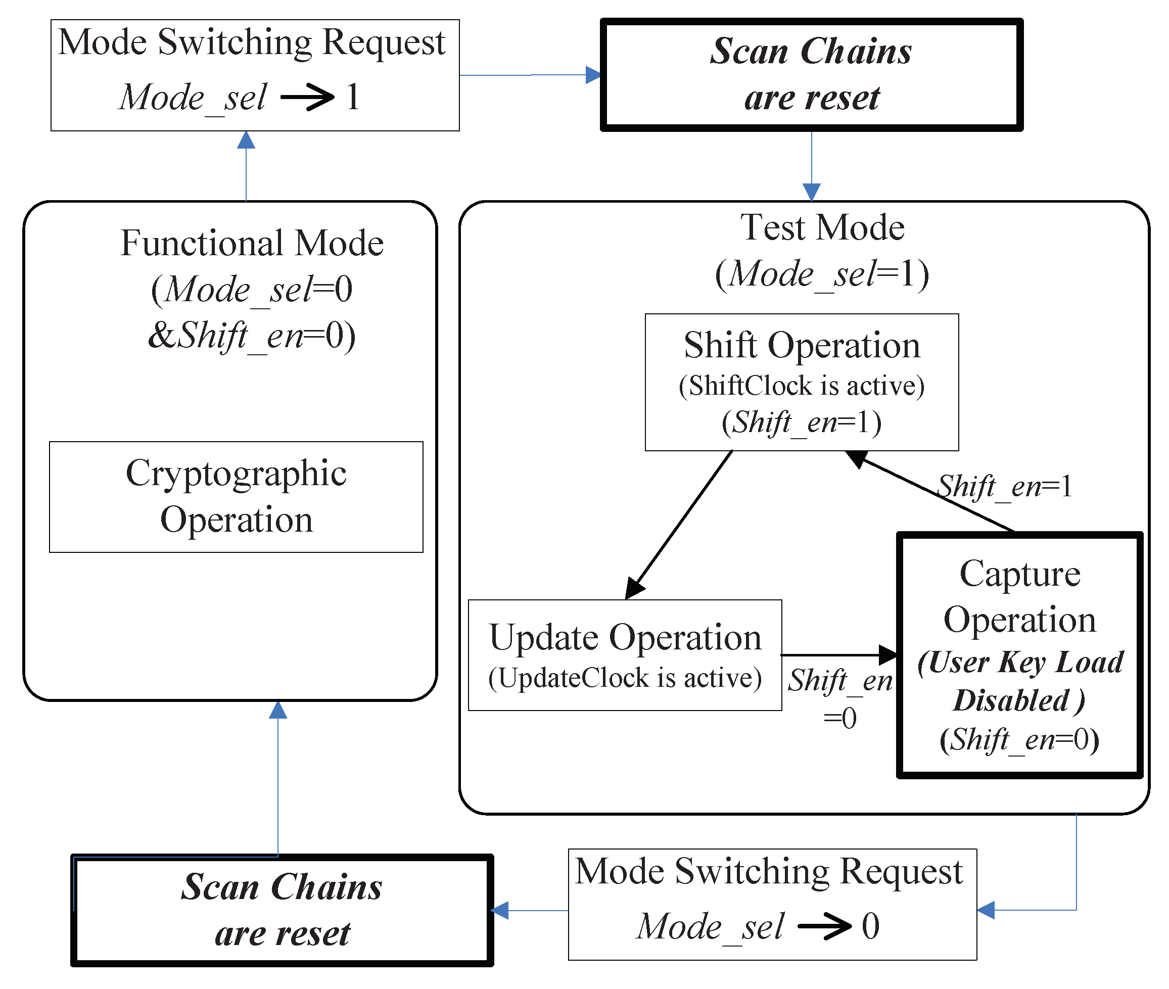
3.2. State Diagram of Proposed Secure Architecture
4. Performance Analysis
4.1. Testability Analysis
4.2. Security Analysis
4.3. Overhead Analysis
5. Conclusions
Author Contributions
Funding
Conflicts of Interest
References
- Qiu, T.; Qiao, R.; Wu, D.O. EABS: An Event-Aware Backpressure Scheduling Scheme for Emergency Internet-of-Things. IEEE. Trans. Mob. Comput. 2018, 17, 72–84. [Google Scholar] [CrossRef]
- Wang, J.; Ju, C.; Gao, Y.; Sangaiah, A.K.; Kim, G.-J. A PSO based Energy Efficient Coverage Control Algorithm for Wireless Sensor Networks, Computers Materials and Continua. Comput. Mater. Contin. 2018, 56, 433–446. [Google Scholar]
- Cao, D.; Zheng, B.; Wang, J.; Ji, B.; Feng, C. Design and analysis of a general relay-node selection mechanism on intersection in vehicular networks. Sensors 2018, 18, 4251. [Google Scholar] [CrossRef] [PubMed]
- Wang, J.; Zhang, Z.; Li, B.; Lee, S.; Sherratt, R.S. An Enhanced Fall Detection System for Elderly Person Monitoring Using Consumer Home Networks. IEEE Trans. Consum. Electron. 2014, 60, 23–29. [Google Scholar] [CrossRef]
- Gao, Y.; Wang, J.; Wu, W.; Sangaiah, A.K.; Lim, S.-J. A Hybrid Method for Mobile Agent Moving Trajectory Scheduling Using ACO and PSO in WSNs. Sensors 2019, 19, 575. [Google Scholar] [CrossRef] [PubMed]
- Shi, F.; Li, Q.; Zhu, T.; Ning, H. A Survey of Data Semantization in Internet-of-Things. Sensors 2018, 18, 313. [Google Scholar] [CrossRef] [PubMed]
- Fortino, G.; Russo, W.; Savaglio, C.; Shen, W.; Zhou, M. Agent-oriented cooperative smart objects: From IoT system design to implementation. IEEE Trans. Syst. Man Cybern. Syst. 2018, 48, 1936–1956. [Google Scholar] [CrossRef]
- Karakaya, A.; Akleylek, S. A Survey on Security Threats and Authentication Approaches in Wireless Sensor Networks. In Proceedings of the International Symposium on Digital Forensic and Security (ISDFS), Antalya, Turkey, 22–25 March 2018; pp. 359–362. [Google Scholar]
- Xiang, L.; Li, Y.; Hao, W.; Yang, P.; Shen, X. Reversible Natural Language Watermarking Using Synonym Substitution and Arithmetic Coding. CMC-Comput. Mater. Contin. 2018, 55, 541–559. [Google Scholar]
- Chen, S.; Zhong, X. Research of Cipher Chip Core for Sensor Data Encryption. IEEE Sens. J. 2016, 16, 4949–4954. [Google Scholar]
- Xu, P.; He, S.; Wang, W.; Susilo, W.; Jin, H. Lightweight Searchable Public-Key Encryption for Cloud-Assisted Wireless Sensor Networks. IEEE Trans. Ind. Inform. 2018, 14, 3712–3723. [Google Scholar] [CrossRef]
- Zhang, Y.; Xu, L.; Dong, Q.; Wang, J.; Blaauw, D.; Sylvester, D. Recryptor: A Reconfigurable Cryptographic Cortex-M0 Processor with In-Memory and Near-Memory Computing for IoT Security. IEEE J. Solid-State Circuits 2018, 53, 995–1005. [Google Scholar] [CrossRef]
- Bahnasawi, M.A.; Ibrahim, K.; Mohamed, A.; Mohamed, M.K.; Moustafa, A.; Abdelmonem, K.; Ismail, Y.; Mostafa, H. ASIC-Oriented Comparative Review of Hardware Security Algorithms for Internet-of-Things Applications. In Proceedings of the IEEE International Conference on Microelectronics (ICM), Giza, Egypt, 17–20 December 2016; pp. 285–288. [Google Scholar]
- Wang, W.; Wang, J.; Wang, Z.; Xiang, L. Access-in-turn test architecture for low-power test application. Int. J. Electron. 2017, 104, 433–441. [Google Scholar] [CrossRef]
- Ahlawat, S.; Tudu, J.; Matrosova, A.; Singh, V. A High Performance Scan Flip-Flop Design for Serial and Mixed Mode Scan Test. IEEE Trans. Device Mater. Rel. 2018, 18, 321–331. [Google Scholar] [CrossRef]
- Wang, L.-T.; Wu, C.-W.; Wen, X. Boundary Scan and Core-Based Testing. In VLSI Test Principles and Architectures; Morgan Kaufmann: San Mateo, CA, USA, 2006; pp. 557–618. [Google Scholar]
- Koeune, F.; Standaert, F.-X. A tutorial on physical security and sidechannel attacks. In Foundations of Security Analysis and Design III; Aldini, A., Gorrieri, R., Martinelli, F., Eds.; Springer: Berlin, Germany, 2005; pp. 78–108. [Google Scholar]
- Yang, B.; Wu, K.; Karri, R. Scan based side channel attack on dedicated hardware implementations of data encryption standard. In Proceedings of the International Test Conference, Charlotte, NC, USA, 26–28 October 2004; pp. 339–344. [Google Scholar]
- Nara, R.; Togawa, N.; Yanagisawa, M.; Ohtsuki, T. Scan-based attack against elliptic curve cryptosystems. In Proceedings of the Asia and South Pacific Design Automation Conference, Taipei, Taiwan, 18–21 January 2010; pp. 407–412. [Google Scholar]
- Nara, R.; Satoh, K.; Yanagisawa, M.; Togawa, N. Scan-based sidechannel attack against RSA cryptosystems using scan signatures. IEICE Trans. Fundam. Electron. Commun. Comput. Sci. 2010, E93-A, 2481–2489. [Google Scholar] [CrossRef]
- Rolt, J.D.; Natale, G.D.; Flottes, M.; Rouzeyre, B. A novel differential scan attack on advanced DFT structures. ACM Trans. Des. Autom. Electron. Syst. 2013, 18, 58. [Google Scholar] [CrossRef]
- Bo, Y.; Kaijie, W.; Karri, R. Secure scan: A design-for-test architecture for crypto chips. IEEE Trans. Comput.-Aided Des. Integr. Circuits Syst. 2006, 25, 2287–2293. [Google Scholar]
- Ali, S.S.; Sinanoglu, O.; Saeed, S.M.; Karri, R. New scan attacks against state-of-the-art countermeasures and DFT. In Proceedings of the IEEE International Workshop Hardware-Oriented Security Trust, Arlington, VA, USA, 6–7 May 2014; pp. 142–147. [Google Scholar]
- Ali, S.S.; Sinanoglu, O.; Karri, R. Test-mode-only scan attack using the boundary scan chain. In Proceedings of the European Test Symposium (ETS), Paderborn, Germany, 26–30 May 2014; pp. 39–44. [Google Scholar]
- Ali, S.S.; Saeed, S.M.; Sinanoglu, O.; Karri, R. Novel test-mode only scan attack and countermeasure for compression-based scan architectures. IEEE Trans. Comput.-Aided Des. Integr. Circuits Syst. 2015, 34, 808–821. [Google Scholar] [CrossRef]
- Novák, O.; Jeníček, J.; Rozkovec, M. Sequential test decompressors with fast variable wide spreading. In Proceedings of the IEEE 19th International Symposium on Design and Diagnostics of Electronic Circuits & Systems, Kosice, Slovakia, 20–22 April 2016; pp. 132–137. [Google Scholar]
- Kang, J.-H.; Touba, N.A.; Yang, J.-S. Reducing control bit overhead for X-masking/X-canceling hybrid architecture via pattern partitioning. In Proceedings of the 53rd ACM/EDAC/IEEE Design Automation Conference, Austin, TX, USA, 5–9 June 2016; pp. 344–349. [Google Scholar]
- Liu, C.; Huang, Y. Effects of embedded decompression and compaction architectures on side-channel attack resistance. In Proceedings of the IEEE VLSI Test Symposium, Berkeley, CA, USA, 6–10 May 2007; pp. 461–468. [Google Scholar]
- Das, A.; Ege, B.; Ghosh, S.; Batina, L.; Verbauwhede, I. Security analysis of industrial test compression schemes. IEEE Trans. Comput.-Aided Des. Integr. Circuits Syst. 2013, 32, 1966–1977. [Google Scholar] [CrossRef]
- Rolt, J.D.; Das, A.; Natale, G.D.; Flottes, M.-L.; Rouzeyre, B.; Verbauwhede, I. Test Versus Security Past and Present. IEEE Trans. Emerg. Top. Comput. 2014, 2, 50–62. [Google Scholar] [CrossRef]
- Hely, D.; Bancel, F.; Flottes, M.-L.; Rouzeyre, B. Securing Scan Control in Crypto Chips. J. Electron. Test. 2007, 23, 457–464. [Google Scholar] [CrossRef]
- Rolt, J.D.; Natale, G.D.; Flottes, M.-L.; Rouzeyre, B. A Smart Test Controller for Scan Chains in Secure Circuits. In Proceedings of the IEEE International On-Line Testing Symposium, Chania, Greece, 8–10 July 2013; pp. 228–229. [Google Scholar]
- Wang, W.Z.; Wang, J.C.; Wang, W.; Liu, P.; Cai, S. A Secure DFT Architecture Protecting Crypto Chips Against Scan-Based Attacks. IEEE Access 2019, 7, 22206–22213. [Google Scholar] [CrossRef]
- Manich, S.; Wamser, M.S.; Guillen, O.M.; Sigl, G. Differential Scan-Path: A Novel Solution for Secure Design-for-Testability. In Proceedings of the International Test Conference, Anaheim, CA, USA, 6–13 September 2013. [Google Scholar]
- Lee, J.; Tehranipoor, M.; Patel, C.; Plusquellic, J. Securing designs against scan-based side-channel attacks. IEEE Trans. Depend. Secure 2007, 4, 325–336. [Google Scholar] [CrossRef]
- Atobe, Y.; Shi, Y.; Yanagisawa, M.; Togawa, N. Secure scan design with dynamically configurable connection. In Proceedings of the 2013 IEEE 19th Pacific Rim International Symposium on Dependable Computing, Vancouver, BC, Canada, 2–4 December 2013; pp. 256–262. [Google Scholar]
- Cui, A.; Luo, Y.; Chang, C.-H. Static and dynamic obfuscations of scan data against scan-based side-channel attacks. IEEE Trans. Inf. Forensics Secur. 2017, 12, 363–376. [Google Scholar] [CrossRef]
- Atobe, Y.; Shi, Y.; Yanagisawa, M.; Togawa, N. Dynamically changeable secure scan architecture against scan-based side channel attack. In Proceedings of the IEEE International SoC Design Conference, Jeju Island, Korea, 4–7 November 2012; pp. 155–158. [Google Scholar]
- Zhang, D.; He, M.; Wang, X.; Tehranipoor, M. Dynamically Obfuscated Scan for Protecting IPs Against Scan-Based Attacks Throughout Supply Chain. In Proceedings of the IEEE 35th VLSI Test Symposium, Las Vegas, NV, USA, 9–12 April 2017; pp. 141–146. [Google Scholar]
- Wang, X.; Zhang, D.; He, M.; Su, D.; Tehranipoor, M. Secure Scan and Test Using Obfuscation throughout Supply Chain. IEEE Trans. Comput.-Aided Des. Integr. Circuits Syst. 2018, 37, 1867–1880. [Google Scholar] [CrossRef]
- Kodera, H.; Yanagisawa, M.; Togawa, N. Scan-based attack against DES cryptosystems using scan signatures. In Proceedings of the IEEE Asia Pacific Conference on Circuits and Systems, Kaohsiung, Taiwan, 2–5 December 2012; pp. 599–602. [Google Scholar]
- Nara, R.; Togawa, N.; Yanagisawa, M.; Ohtsuki, T. A scan-based attack based on discriminators for AES cryptosystems. IEICE Trans. Fundam. Electron. Commun. Comput. Sci. 2009, E92-A, 3229–3237. [Google Scholar] [CrossRef]
- Vaghani, D.; Ahlawat, S.; Tudu, J.; Fujita, M.; Singh, V. On Securing Scan Design Through Test Vector Encryption. In Proceedings of the IEEE International Symposium on Circuits and Systems, Florence, Italy, 27–30 May 2018; pp. 466–470. [Google Scholar]
- Silva, M.D.; Flottes, M.-L.; Natale, G.D.; Rouzeyre, B. Preventing Scan Attacks on Secure Circuits through Scan Chain Encryption. IEEE Trans. Comput.-Aided Des. Integr. Circuits Syst. 2019, 38, 538–550. [Google Scholar] [CrossRef]
- Mangard, S.; Aigner, M.; Dominikus, S. A highly regular and scalable AES hardware architecture. IEEE Trans. Comput. 2004, 52, 483–491. [Google Scholar] [CrossRef]
- AES: Overview. Available online: http://opencores.org (accessed on 30 October 2014).
- Verbauwhede, I.; Schaumont, P.; Kuo, H. Design and performance testing of a 2.29-GB/s Rijndael processor. IEEE J. Solid-State Circuits 2003, 38, 569–572. [Google Scholar] [CrossRef]
- Hely, D.; Flottes, M.-L.; Bancel, F.; Rouzeyre, B.; Bérard, N.; Renovell, M. Scan Design and Secure Chip. In Proceedings of the IEEE International On-Line Testing Symposium, Funchal, Madeira Island, Portugal, 12–14 July 2004; pp. 219–226. [Google Scholar]

| A1 A2 | A1’ A2’ | |
|---|---|---|
| 1 | 00 | 11 |
| 1 | 01 | 01 |
| 1 | 10 | 10 |
| 1 | 11 | 11 |
| 0 | 00 | 00 |
| 0 | 01 | 01 |
| 0 | 10 | 10 |
| 0 | 11 | 11 |
| AES | Standard Scan Design | Proposed Secure Architecture | ||||
|---|---|---|---|---|---|---|
| Test Vectors | Fault Coverage | Test Vectors | Test Vectors Changed | Fault Coverage | Fault Coverage Changed | |
| Pipelined | 903 | 97.26% | 910 | +0.78% | 97.23% | −0.03% |
| Iterative | 608 | 97.90% | 611 | +0.49% | 97.88% | −0.02% |
| AES | Architecture | Area | Area Overhead | ||
|---|---|---|---|---|---|
| Original | Standard | Proposed | Overhead | Ratio | |
| Pipelined | 205,934 | 217,720 | 217,804 | 84 | 0.039% |
| Iterative | 25,052 | 29,032 | 29,053 | 21 | 0.072% |
| AES | Area Overhead Ratio | ||||||
|---|---|---|---|---|---|---|---|
| Proposed | MKR [22] | Secure | SOSD [37] | DOS [40] | |||
| DFT [33] | SOSD-64 | SOSD-128 | DOS-10% | DOS-30% | |||
| Pipelined | 0.039% | 0.15% | 0.11% | 0.18% | 0.34% | 0.85% | 2.01% |
| Iterative | 0.072% | 1.32% | 0.96% | 1.52% | 2.81% | - | - |
| Scheme | Security | Impact on | Impact on Test | ||
|---|---|---|---|---|---|
| Vulnerability (*) | Probability of Brute Force | IP Design | Test Time | Test Application | |
| Proposed | None | Brute force is inapplicable | A D flip-flop and a few logic gates insertion; no introduction of extra input signals | No extra cycles are needed | Online testing cannot be applied |
| MKR [22] | Test-mode-only attacks for boundary scan design | Brute force is inapplicable | Secure control circuit insertion; scan chain modification; extra control signals introduction | No extra cycles are needed | Online testing cannot be applied |
| Mode reset [31] | Test-mode-only attacks for boundary scan design | Brute force is inapplicable | System mode security manager, scan_enable integrity controller, reset controller and test controller insertion | No extra cycles are needed | Online testing cannot be applied |
| Smart controller [32] | Test-mode-only attacks for boundary scan design | Brute force is inapplicable | Smart controller and multiple multiplexers insertion | No extra cycles are needed | Online testing cannot be applied |
| Secure DFT [33] | Test-mode-only attacks for boundary scan design | Brute force is inapplicable | A small secure test controller and a few logic gates insertion | No extra cycles are needed | Online testing cannot be applied |
| SOSD-64 [37] | None | Test key loading controller, shift register insertion; scan-enabling input modification in scan chains | 64 clock cycles before testing | Delay test based on LoC cannot be applied | |
| SOSD-128 [37] | None | Test key loading controller, shift register insertion; scan-enabling input modification in scan chains | 128 clock cycles before testing | Delay test based on LoC cannot be applied | |
| DOS [40] | None | (**) | LFSR, shadow chain and control unit insertion; scan chain modification | No extra cycles are needed | All the tests can be applied |
| Scan chain encryption [44] | None | (***) | Scan cipher insertion at scan inputs and outputs | multiple clock cycles for pattern decryption | All the tests can be applied |
| Scan chain scrambling [48] | None | (****) | Test configuration module, unpredictable number generator and multiple multiplexers insertion; scan chain modification | Immaterial | All the tests can be applied |
© 2019 by the authors. Licensee MDPI, Basel, Switzerland. This article is an open access article distributed under the terms and conditions of the Creative Commons Attribution (CC BY) license (http://creativecommons.org/licenses/by/4.0/).
Share and Cite
Wang, W.; Deng, Z.; Wang, J. Enhancing Sensor Network Security with Improved Internal Hardware Design. Sensors 2019, 19, 1752. https://doi.org/10.3390/s19081752
Wang W, Deng Z, Wang J. Enhancing Sensor Network Security with Improved Internal Hardware Design. Sensors. 2019; 19(8):1752. https://doi.org/10.3390/s19081752
Chicago/Turabian StyleWang, Weizheng, Zhuo Deng, and Jin Wang. 2019. "Enhancing Sensor Network Security with Improved Internal Hardware Design" Sensors 19, no. 8: 1752. https://doi.org/10.3390/s19081752
APA StyleWang, W., Deng, Z., & Wang, J. (2019). Enhancing Sensor Network Security with Improved Internal Hardware Design. Sensors, 19(8), 1752. https://doi.org/10.3390/s19081752