Towards Portable Nanophotonic Sensors


Abstract
1. Introduction
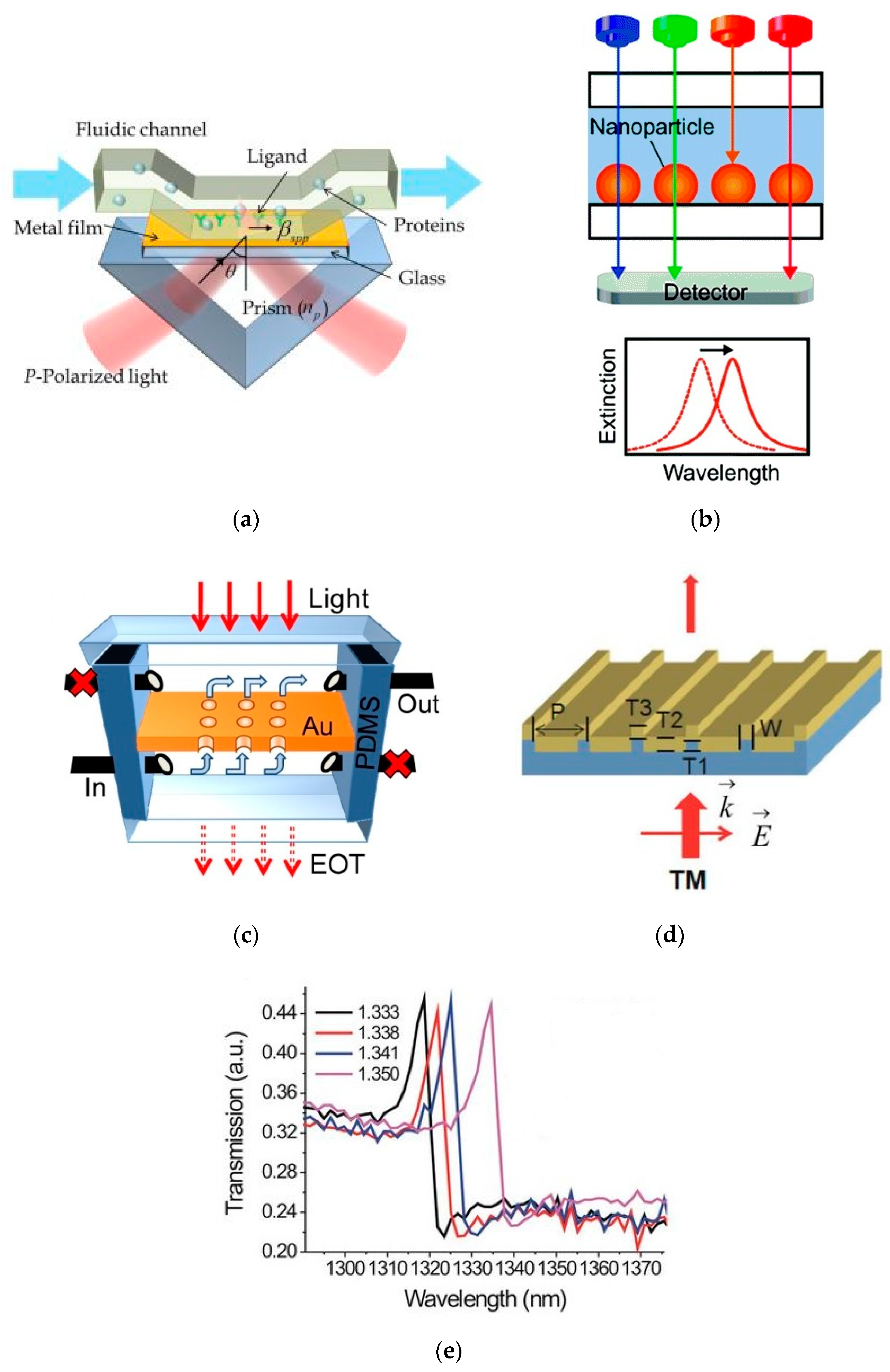
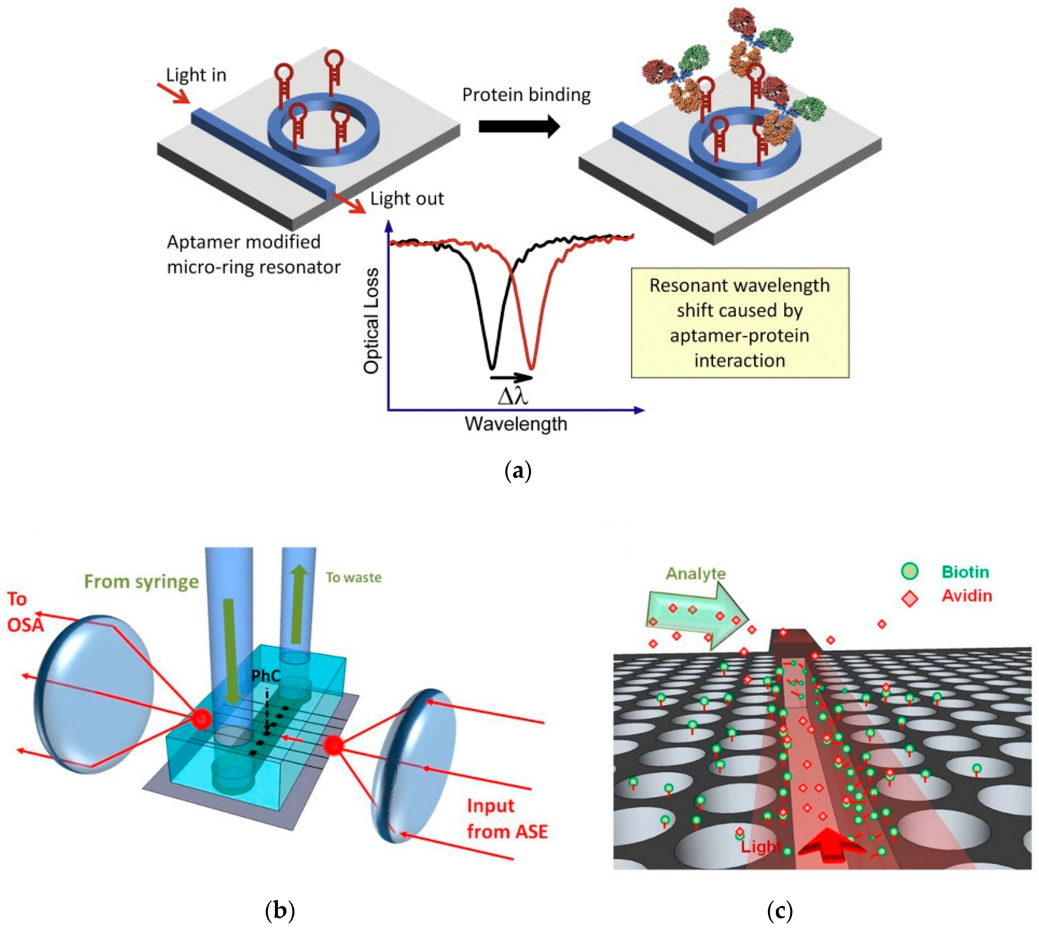
2. On Chip Nanophotonic Sensors
2.1. Metal-Plasmonic Nanophotonic Sensors
2.2. On Chip Semiconductor/Dielectric Nanophotonic Sensors
3. Nanophotonic Sensors with Compact Readout System
3.1. Nanophotonic Sensors having Monolithically Integrated Readout System
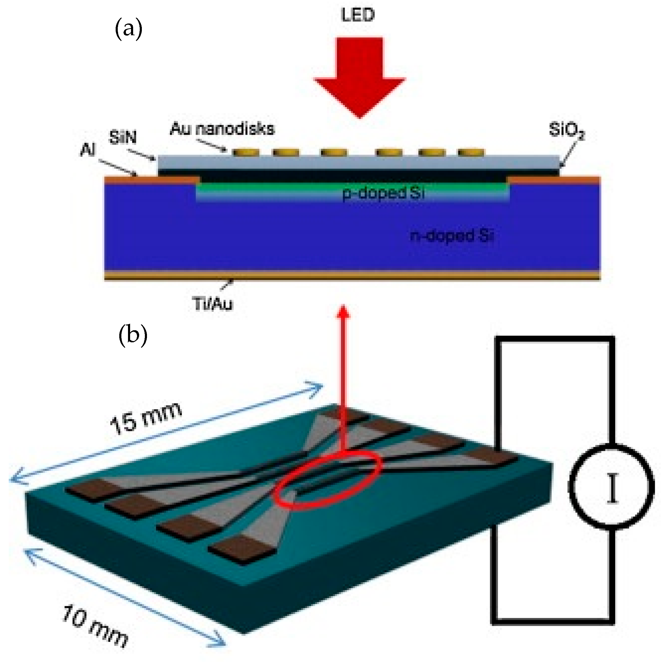
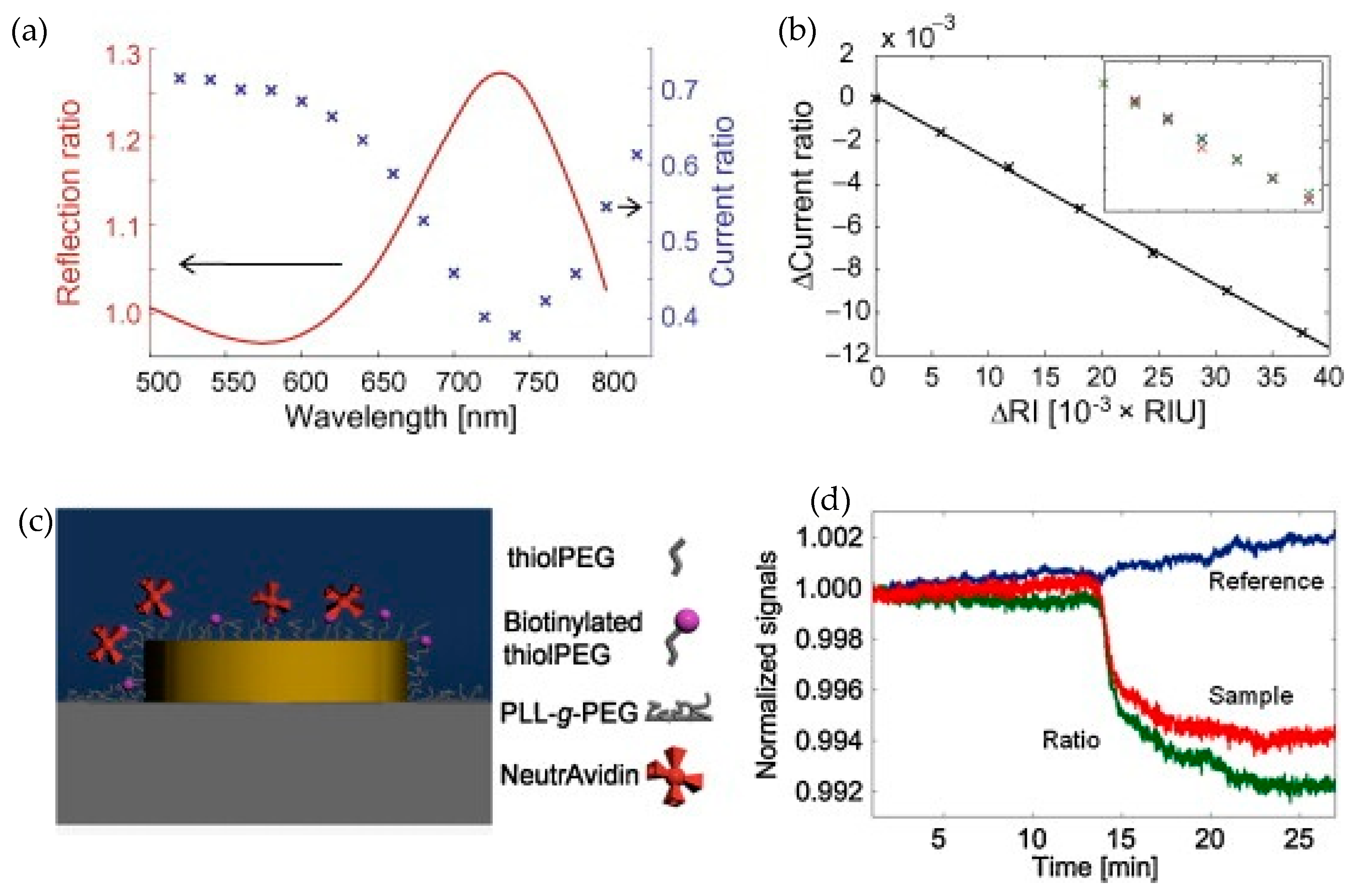
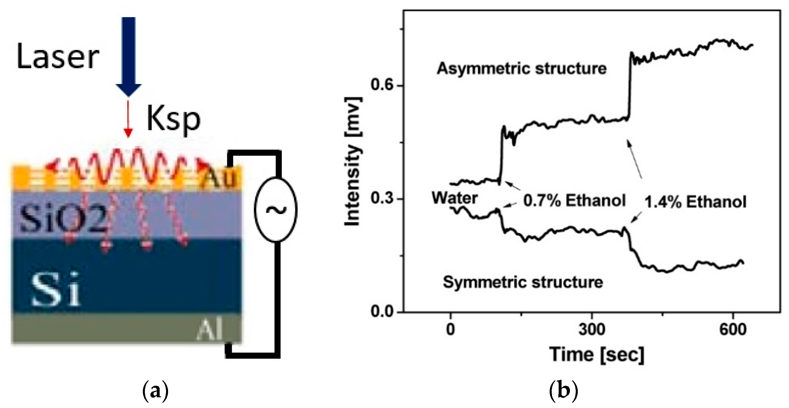
3.1.1. Nanophotonic Sensors with Integrated Silicon Photodiode
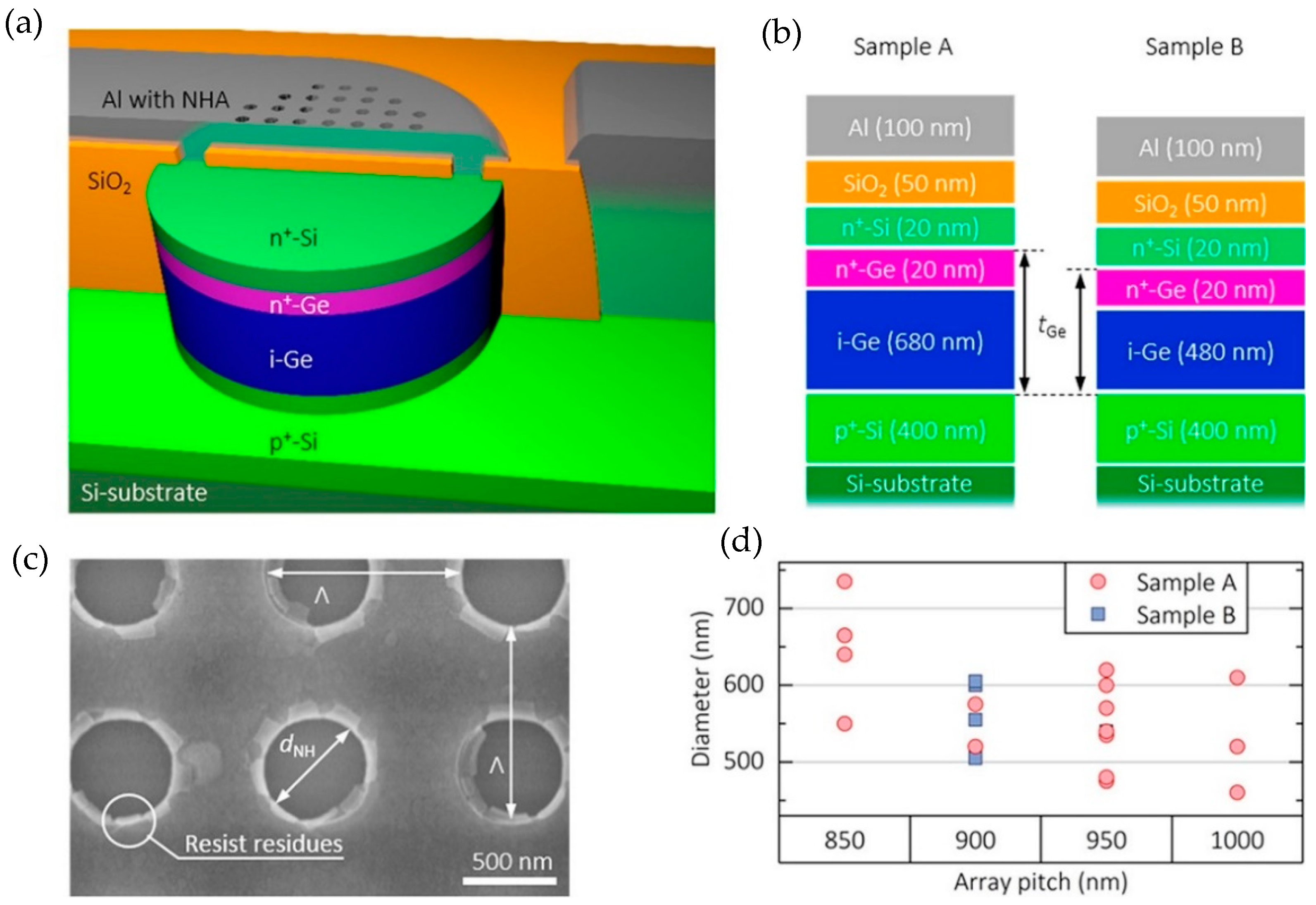
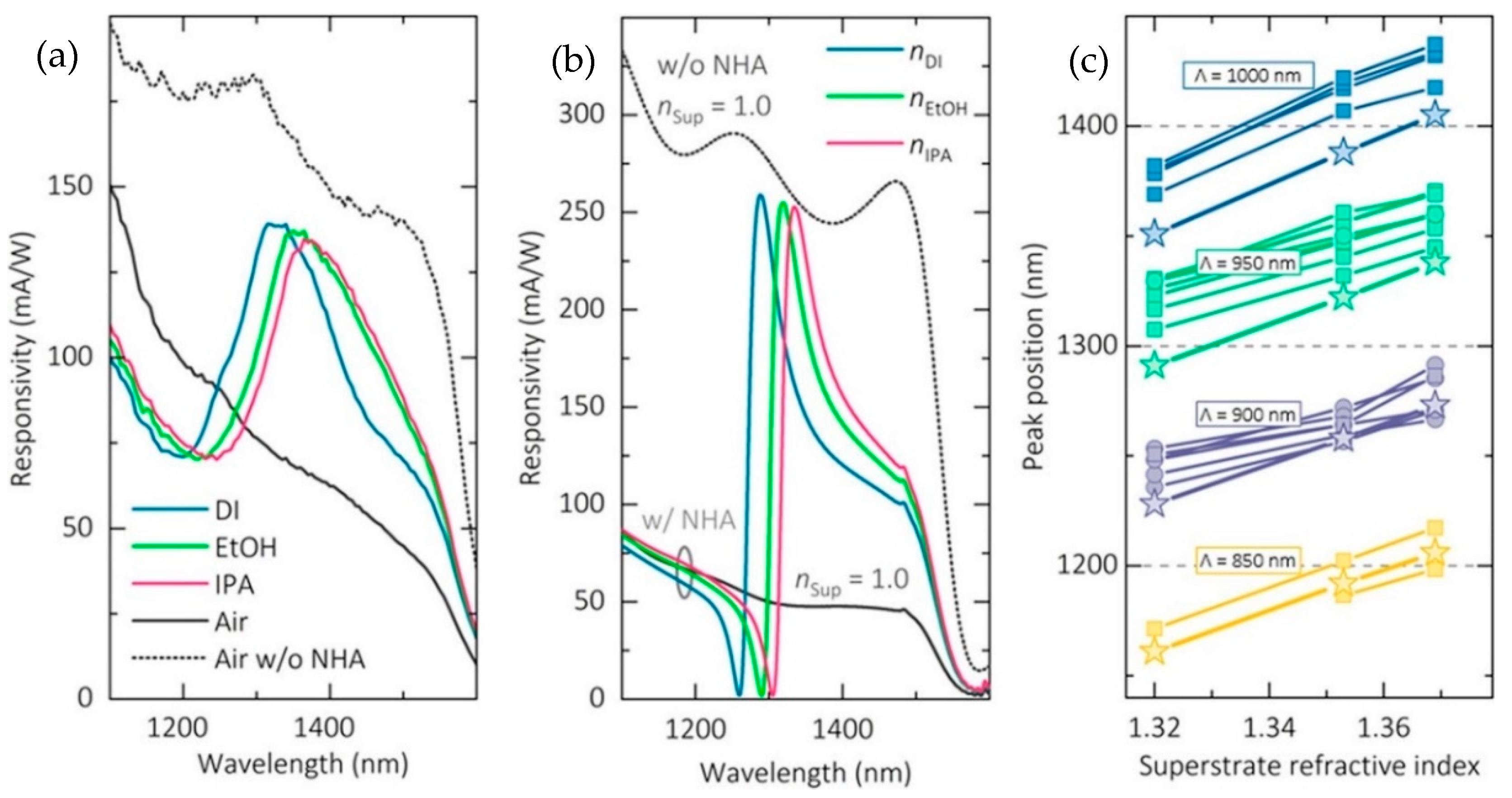
3.1.2. Nanophotonic Sensor with Integrated Germanium Pin Photodiode
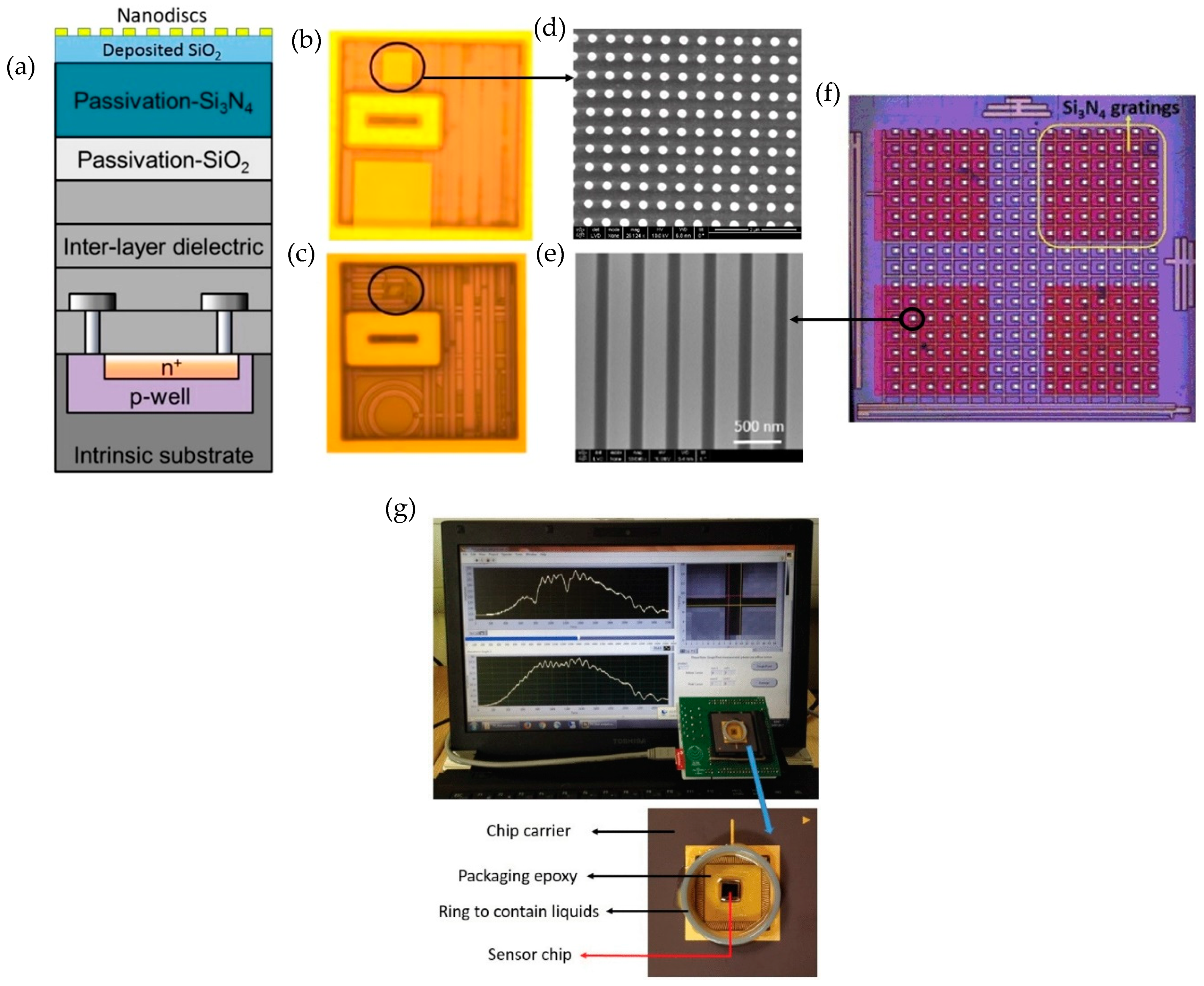
3.1.3. Nanophotonic Sensor Integrated with CMOS Technology
3.2. Nanophotonic Sensors with Compact but Separate Readout System
3.2.1. Nanophotonic Sensor Based on CMOS/CCD Imager for Readout
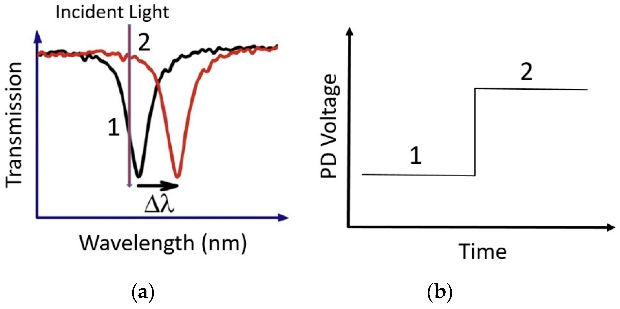
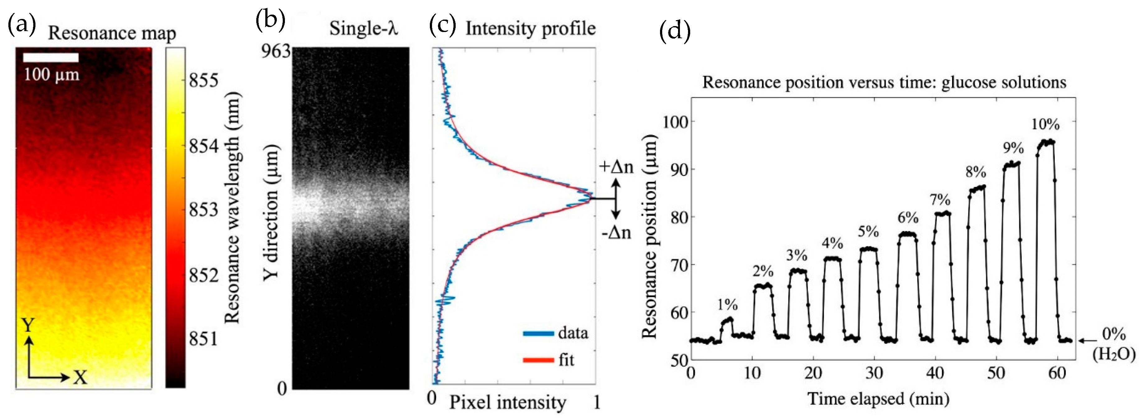
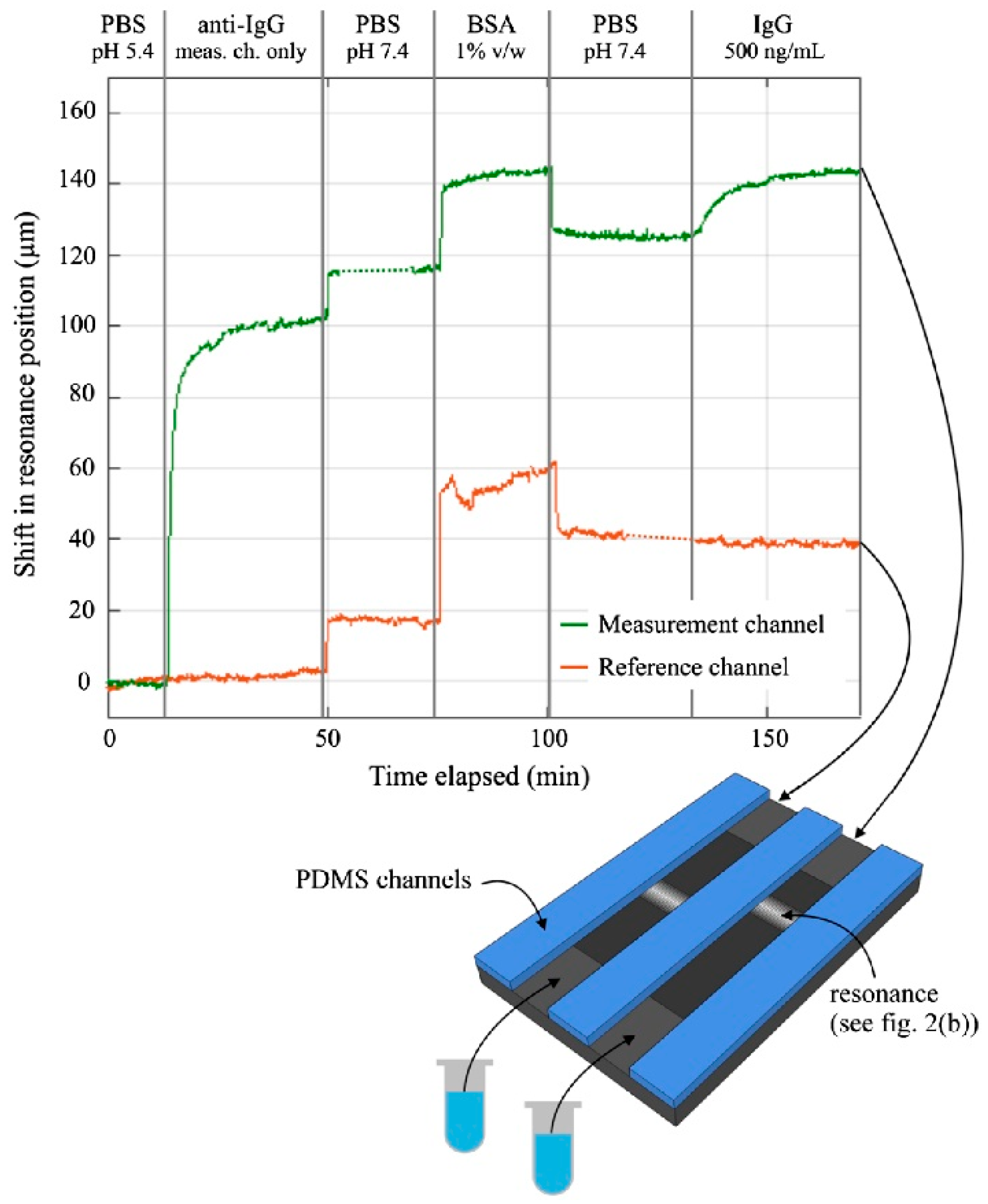
3.2.2. Self-Readout of Nanophotonic Sensor Based on Chirped Gratings and Camera
4. Summary
5. Conclusions and Outlook
Funding
Conflicts of Interest
References
- Tokel, O.; Inci, F.; Demirci, U. Advances in plasmonic technologies for point of care applications. Chem. Rev. 2014, 114, 5728–5752. [Google Scholar] [CrossRef]
- Brolo, A.G. Plasmonics for future biosensors. Nat. Photonics 2012, 6, 709–713. [Google Scholar] [CrossRef]
- Joshi, G.K.; Deitz-McElyea, S.; Johnson, M.; Mali, S.; Korc, M.; Sardar, R. Highly specific plasmonic biosensors for ultrasensitive micro-RNA detection in plasma from pancreatic cancer patients. Nano Lett. 2014, 14, 6955–6963. [Google Scholar] [CrossRef] [PubMed]
- Brolo, A.G.; Gordon, R.; Leathem, B.; Kavanagh, K.L. Surface plasmon sensor based on the enhanced light transmission through arrays of nanoholes in gold films. Langmuir 2004, 20, 4813–4815. [Google Scholar] [CrossRef] [PubMed]
- De Leebeeck, A.; Kumar, L.K.S.; de Lange, V.; Sinton, D.; Gordon, R.; Brolo, A.G. On-chip surface-based detection with nanohole arrays. Anal. Chem. 2007, 79, 4094–4100. [Google Scholar] [CrossRef]
- Lee, K.L.; Lee, C.W.; Wang, W.S.; Wei, P.K. Sensitive biosensor array using surface plasmon resonance on metallic nanoslits. J. Biomed. Opt. 2007, 12, 044023. [Google Scholar] [CrossRef]
- Sreekanth, K.V.; Alapan, Y.; ElKabbash, M.; Ilker, E.; Hinczewski, M.; Gurkan, U.A.; Luca, A.D.; Strangi, G. Extreme sensitivity biosensing platform based on hyperbolic metamaterials. Nat. Mater. 2016, 15, 621–627. [Google Scholar] [CrossRef]
- Sreekanth, K.V.; Alapan, Y.; ElKabbash, M.; Wen, A.M.; Ilker, E.; Hinczewski, M.; Gurkan, U.A.; Steinmetz, N.F.; Strangi, G. Enhancing the Angular Sensitivity of Plasmonic Sensors Using Hyperbolic Metamaterials. Adv. Opt. Mater. 2016, 4, 1767–1772. [Google Scholar] [CrossRef]
- Khanikev, A.B.; Wu, C.; Shevets, G. Fano-resonant metamaterials and their applications. Nanophotonics 2013, 2, 247–264. [Google Scholar] [CrossRef]
- Luk’yanchuk, B.; Zheludev, N.I.; Maier, S.A.; Halas, N.J.; Nordlander, P.; Giessen, H.; Chong, C.T. The Fano resonance in plasmonic nanostructures and metamaterials. Nat. Mater. 2010, 9, 707–715. [Google Scholar] [CrossRef] [PubMed]
- Schipper, E.; Brugman, A.; Dominguez, C.; Lechuga, L.; Kooyman, R.; Greve, J. The realization of an integrated Mach–Zehnder waveguide immunosensor in silicon technology. Sens. Actuators B Chem. 1997, 40, 147–153. [Google Scholar] [CrossRef]
- Heideman, R.; Kooyman, R.; Greve, J. Performance of a highly sensitive optical waveguide Mach–Zehnder interferometer immunosensor. Sens. Actuators B Chem. 1993, 10, 209–217. [Google Scholar] [CrossRef]
- Crespi, A.; Gu, Y.; Ngamsom, B.; Hoekstra, H.J.; Dongre, C.; Pollnau, M.; Ramponi, R.; van den Vlekkert, H.H.; Watts, P.; Cerullo, G.; et al. Three-dimensional Mach–Zehnder interferometer in a microfluidic chip for spatially-resolved label-free detection. Lab Chip 2010, 10, 1167–1173. [Google Scholar] [CrossRef] [PubMed]
- Shew, B.; Cheng, Y.; Tsai, Y. Monolithic SU-8 micro-interferometer for biochemical detections. Sens. Actuators A Phys. 2008, 141, 299–306. [Google Scholar] [CrossRef]
- Baehr-Jones, T.; Hochberg, M.; Walker, C.; Scherer, A. High-Q optical resonators in silicon-on-insulator-based slot waveguides. Appl. Phys. Lett. 2005, 86, 081101. [Google Scholar] [CrossRef]
- Barrios, C.A.; Gylfason, K.B.; Sánchez, B.; Griol, A.; Sohlström, H.; Holgado, M.; Casquel, R. Slot-waveguide biochemical sensor. Opt. Lett. 2007, 32, 3080–3082. [Google Scholar] [CrossRef] [PubMed]
- Taniguchi, T.; Hirowatari, A.; Ikeda, T.; Fukuyama, M.; Amemiya, Y.; Kuroda, A.; Yokoyama, S. Detection of antibody-antigen reaction by silicon nitride slot-ring biosensors using protein G. Opt. Commun. 2016, 365, 16–23. [Google Scholar] [CrossRef]
- Di Falco, A.; O’faolain, L.; Krauss, T. Chemical sensing in slotted photonic crystal heterostructure cavities. Appl. Phys. Lett. 2009, 94, 063503. [Google Scholar] [CrossRef]
- Ksendzov, A.; Lin, Y. Integrated optics ring-resonator sensors for protein detection. Opt. Lett. 2005, 30, 3344–3346. [Google Scholar] [CrossRef]
- Krioukov, E.; Klunder, D.; Driessen, A.; Greve, J.; Otto, C. Sensor based on an integrated optical microcavity. Opt. Lett. 2002, 27, 512–514. [Google Scholar] [CrossRef]
- Armani, A.M.; Vahala, K.J. Heavy water detection using ultra-high-Q microcavities. Opt. Lett. 2006, 31, 1896–1898. [Google Scholar] [CrossRef]
- Wu, C.; Khanikaev, A.B.; Adato, R.; Arju, N.; Yanik, A.A.; Altug, H.; Shvets, G. Fano-resonant asymmetric metamaterials for ultrasensitive spectroscopy and identification of molecular monolayers. Nat. Mater. 2012, 11, 69–75. [Google Scholar] [CrossRef]
- Kabashin, A.V.; Evans, P.; Pastkovsky, S.; Hendren, W.; Wurtz, G.A.; Atkinson, R.; Pollard, R.; Podolskiy, V.A.; Zayats, A.V. Plasmonic nanorod metamaterials for biosensing. Nat. Mater. 2009, 8, 867–871. [Google Scholar] [CrossRef]
- Brandenburg, A.; Krauter, R.; Künzel, C.; Stefan, M.; Schulte, H. Interferometric sensor for detection of surface-bound bioreactions. Appl. Opt. 2000, 39, 6396–6405. [Google Scholar] [CrossRef]
- Schmitt, K.; Schirmer, B.; Hoffmann, C.; Brandenburg, A.; Meyrueis, P. Interferometric biosensor based on planar optical waveguide sensor chips for label-free detection of surface bound bioreactions. Biosens. Bioelectron. 2007, 22, 2591–2597. [Google Scholar] [CrossRef]
- Im, H.; Shao, H.; Park, Y.I.; Peterson, V.M.; Castro, C.M.; Weissleder, R.; Lee, H. Label-free detection and molecular profiling of exosomes with a nano-plasmonic sensor. Nat. Biotechnol. 2014, 32, 490–495. [Google Scholar] [CrossRef]
- Fernández, F.; Hegnerová, K.; Piliarik, M.; Sanchez-Baeza, F.; Homola, J.; Marco, M.P. A label-free and portable multichannel surface plasmon resonance immunosensor for on site analysis of antibiotics in milk samples. Biosens. Bioelectron. 2010, 26, 1231–1238. [Google Scholar] [CrossRef]
- Piliarik, M.; Bocková, M.; Homola, J. Surface plasmon resonance biosensor for parallelized detection of protein biomarkers in diluted blood plasma. Biosens. Bioelectron. 2010, 26, 1656–1661. [Google Scholar] [CrossRef]
- Haes, A.J.; Zou, S.; Zhao, J.; Schatz, G.C.; Van Duyne, R.P. Localized Surface Plasmon Resonance Spectroscopy near Molecular Resonances. J. Am. Chem. Soc. 2006, 128, 10905–10914. [Google Scholar] [CrossRef]
- Anker, J.N.; Hall, W.P.; Lyandres, O.; Shah, N.C.; Zhao, J.; Van Duyne, R.P. Biosensing with Plasmonic Nanosensors. Nat. Mater. 2008, 7, 442–453. [Google Scholar] [CrossRef]
- Lesuffleur, A.; Im, H.; Lindquist, N.C.; Lim, K.S.; Oh, S.H. Laser-illuminated nanohole arrays for multiplex plasmonic microarray sensing. Opt. Express 2008, 16, 219–224. [Google Scholar] [CrossRef]
- Fernández Gavela, A.; Grajales García, D.; Ramirez, J.; Lechuga, L. Last advances in silicon-based optical biosensors. Sensors 2016, 16, 285. [Google Scholar] [CrossRef]
- Zinoviev, K.E.; González-Guerrero, A.B.; Domínguez, C.; Lechuga, L.M. Integrated bimodal waveguide interferometric biosensor for label-free analysis. J. Lightwave Technol. 2011, 29, 1926–1930. [Google Scholar] [CrossRef]
- Densmore, A.; Xu, D.X.; Janz, S.; Waldron, P.; Mischki, T.; Lopinski, G.; Delâge, A.; Lapointe, J.; Cheben, P.; Lamontagne, B.; et al. Spiral-path high-sensitivity silicon photonic wire molecular sensor with temperature-independent response. Opt. Lett. 2008, 33, 596–598. [Google Scholar] [CrossRef]
- De Vos, K.; Bartolozzi, I.; Schacht, E.; Bienstman, P.; Baets, R. Silicon-on-Insulator microring resonator for sensitive and label-free biosensing. Opt. Express 2007, 15, 7610–7615. [Google Scholar] [CrossRef]
- Ciminelli, C.; Dell’Olio, F.; Conteduca, D.; Campanella, C.; Armenise, M. High performance SOI microring resonator for biochemical sensing. Opt. Laser Technol. 2014, 59, 60–67. [Google Scholar] [CrossRef]
- Lee, M.R.; Fauchet, P.M. Two-dimensional silicon photonic crystal based biosensing platform for protein detection. Opt. Express 2007, 15, 4530–4535. [Google Scholar] [CrossRef]
- Lee, S.; Eom, S.C.; Chang, J.S.; Huh, C.; Sung, G.Y.; Shin, J.H. Label-free optical biosensing using a horizontal air-slot SiNx microdisk resonator. Opt. Express 2010, 18, 20638–20644. [Google Scholar] [CrossRef]
- Tu, X.; Song, J.; Liow, T.Y.; Park, M.K.; Yiying, J.Q.; Kee, J.S.; Yu, M.; Lo, G.Q. Thermal independent silicon-nitride slot waveguide biosensor with high sensitivity. Opt. Express 2012, 20, 2640–2648. [Google Scholar] [CrossRef]
- Liu, Q.; Tu, X.; Kim, K.W.; Kee, J.S.; Shin, Y.; Han, K.; Yoon, Y.J.; Lo, G.Q.; Park, M.K. Highly sensitive Mach-Zehnder interferometer biosensor based on silicon nitride slot waveguide. Sens. Actuators B Chem. 2013, 188, 681–688. [Google Scholar] [CrossRef]
- Chao, C.Y.; Fung, W.; Guo, L.J. Polymer microring resonators for biochemical sensing applications. IEEE J. Sel. Top. Quantum Electron. 2006, 12, 134–142. [Google Scholar] [CrossRef]
- Girault, P.; Lorrain, N.; Poffo, L.; Guendouz, M.; Lemaitre, J.; Carré, C.; Gadonna, M.; Bosc, D.; Vignaud, G. Integrated polymer micro-ring resonators for optical sensing applications. J. Appl. Phys. 2015, 117, 104504. [Google Scholar] [CrossRef]
- Tetz, K.A.; Pang, L.; Fainman, Y. High-resolution surface plasmon resonance sensor based on linewidth-optimized nanohole array transmittance. Opt. Lett. 2006, 31, 1528–1530. [Google Scholar] [CrossRef]
- Zafar, R.; Salim, M. Enhnaced figure of merit in Fano resonance-based plasmonic refractive index sensor. IEEE Sens. J. 2015, 15, 6313–6316. [Google Scholar] [CrossRef]
- Bao, K.; Mirin, N.A.; Nordlander, P. Fano resonances in planar silber nanosphere clusters. Appl. Phys. A 2010, 100, 333–339. [Google Scholar] [CrossRef]
- Mirin, N.A.; Bao, K.; Nordlander, P. Fano resonances in plasmonic nanoparticle aggregates. J. Phys. Chem. A 2009, 113, 4028–4034. [Google Scholar] [CrossRef]
- Luan, E.; Yun, H.; Laplatine, L.; Dattner, Y.; Ratner, D.M.; Cheung, K.; Chrostowski, L. Enhanced sensitivity of sub-wavelength multi-box waveguide microring resonator label-free biosensor. IEEE J. Sel. Top. Quantum Electron. 2019, 25, 1–11. [Google Scholar] [CrossRef]
- Armani, A.M.; Kulkarni, R.P.; Fraser, S.E.; Flagan, R.C.; Vahala, K.J. Label-free, single-molecule detection with optical microcavities. Science 2007, 317, 783–787. [Google Scholar] [CrossRef]
- Grist, S.M.; Schmidt, S.A.; Flueckiger, J.; Donzella, V.; Shi, W.; Fard, S.T.; Kirk, J.T.; Ratner, D.M.; Cheung, K.C.; Chrostowski, L. Silicon photonic micro-disk resonators for label-free biosensing. Opt. Express 2013, 21, 7994–8006. [Google Scholar] [CrossRef]
- Zlatanovic, S.; Mirkarimi, L.W.; Sigalas, M.M.; Bynum, M.A.; Chow, E.; Robotti, K.M.; Burr, G.W.; Esener, S.; Grot, A. Photonic crystal microcavity sensor for ultracompact monitoring of reaction kinetics and protein concentration. Sens. Actuators B 2009, 141, 13–19. [Google Scholar] [CrossRef]
- Dorfner, D.; Zabel, T.; Hurlimann, T.; Hauke, N.; Frandsen, L.; Rant, U.; Abstreiter, G.; Finley, J. Photonic crystal nanostructures for optical biosensing applications. Biosens. Bioelectron. 2009, 24, 3688–3692. [Google Scholar] [CrossRef]
- Mandal, S.; Serey, X.; Erickson, D. Nanomanipulation using silicon photonic crystal resonators. Nano Lett. 2009, 10, 99–104. [Google Scholar] [CrossRef]
- Shi, Y.; Ma, K.; Dai, D. Sensitivity Enhancement in Si Nanophotonic Waveguides Used for Refractive Index Sensing. Sensors 2016, 16, 324. [Google Scholar] [CrossRef]
- Barrios, C.A. Optical Slot-Waveguide Based Biochemical Sensors. Sensors 2009, 9, 4751–4765. [Google Scholar] [CrossRef]
- Mukundan, H.; Anderson, A.S.; Grace, W.K.; Grace, K.M.; Hartman, N.; Martinez, J.S.; Swanson, B.I. Waveguide-Based Biosensors for Pathogen Detection. Sensors 2009, 9, 5783–5809. [Google Scholar] [CrossRef]
- Dell’Olio, F.; Passaro, V.M. Optical Sensing by Optimized Silicon Slot Waveguides. Opt. Express 2007, 15, 4977. [Google Scholar] [CrossRef]
- Gonzalez-Guerrero, A.B.; Osmond, J.; Zinoviev, K.; Sepulveda, B.; Dominguez, C.; Dante, S.; Duval, D.; Lechuga, L.M. Towards a complete lab-on-chip system using integrated Mach-Zehnder interferometers. Opt. Pure Appl. 2012, 45, 87–95. [Google Scholar]
- Heideman, R.; Kooyman, R.; Greve, J. Development of an optical waveguide interferometric immunosensor. Sens. Actuators B Chem. 1991, 4, 297–299. [Google Scholar] [CrossRef]
- Heideman, R.; Lambeck, P. Remote opto-chemical sensing with extreme sensitivity: Design, fabrication and performance of a pigtailed integrated optical phase-modulated Mach–Zehnder interferometer system. Sens. Actuators B Chem. 1999, 61, 100–127. [Google Scholar] [CrossRef]
- Jugessur, A.; Dou, J.; Aitchison, J.; De La Rue, R.; Gnan, M. A photonic nano-Bragg grating device integrated with microfluidic channels for bio-sensing applications. Microelectron. Eng. 2009, 86, 1488–1490. [Google Scholar] [CrossRef]
- Prabhathan, P.; Murukeshan, V.; Jing, Z.; Ramana, P.V. Compact SOI nanowire refractive index sensor using phase shifted Bragg grating. Opt. Express 2009, 17, 15330–15341. [Google Scholar] [CrossRef]
- Schmid, J.H.; Sinclair, W.; García, J.; Janz, S.; Lapointe, J.; Poitras, D.; Li, Y.; Mischki, T.; Lopinski, G.; Cheben, P.; et al. Silicon on-Insulator Guided Mode Resonant Grating for Evanescent Field Molecular Sensing. Opt. Express 2009, 17, 18371. [Google Scholar] [CrossRef]
- Sun, T.; Kan, S.; Marriott, G.; Chang-Hasnain, C. High-Contrast Grating Resonators for Label-Free Detection of Disease Biomarkers. Sci. Rep. 2016, 6, 27482. [Google Scholar] [CrossRef]
- Shakoor, A.; Grande, M.; Grant, J.; Cumming, D.R.S. One-dimensional silicon nitride grating refractive index sensor suitable for integration with CMOS detectors. IEEE Photonics J. 2017, 9, 1–11. [Google Scholar] [CrossRef]
- White, I.M.; Fan, X. On the Performance Quantification of Resonant Refractive Index Sensors. Opt. Express 2008, 16, 1020. [Google Scholar] [CrossRef]
- GE Healhtcare. Biacore. 2006. Available online: https://www.biacore.com/lifesciences/index.html (accessed on 14 March 2019).
- Genalyte. Genalyte. 2009. Available online: https://www.genalyte.com (accessed on 14 March 2019).
- Mazzotta, F.; Wang, G.; Hägglund, C.; Höök, F.; Jonsson, M.P. Nanoplasmonic biosensing with on-chip electrical detection. Biosens. Bioelectron. 2010, 26, 1131–1136. [Google Scholar] [CrossRef]
- Guyot, L.; Blanchard-Dionne, A.-P.; Patskovsky, S.; Meunier, M. Integrated silicon-based nanoplasmonic sensor. Opt. Express 2011, 19, 9962–9967. [Google Scholar] [CrossRef]
- Patskovsky, S.; Meunier, M. Integrated Si-based nanoplasmonic sensor with phase-sensitive angular interrogation. Ann. Phys. 2013, 525, 431–436. [Google Scholar] [CrossRef]
- Perino, M.; Pasqualotto, E.; De Toni, A.; Garoli, D.; Scaramuzza, M.; Zilio, P.; Ongarello, T.; Paccagnella, A.; Romanato, F. Development of a complete plasmonic grating-based sensor and its application for self-assembled monolayer detection. Appl. Opt. 2014, 53, 5969–5976. [Google Scholar] [CrossRef]
- Turker, B.; Guner, H.; Ayas, S.; Ekiz, O.O.; Acar, H.; Guler, M.O.; Dâna, A. Grating coupler integrated photodiodes for plasmon resonance based sensing. Lab Chip 2011, 11, 282–287. [Google Scholar] [CrossRef]
- Augel, L.; Kawaguchi, Y.; Bechler, S.; Körner, R.; Schulze, J.; Uchida, H.; Fischer, I.A. Integrated Collinear Refractive Index Sensor with Ge PIN Photodiodes. ACS Photonics 2018, 5, 4586–4593. [Google Scholar] [CrossRef]
- Shakoor, A.; Cheah, B.C.; Hao, D.; Al-Rawhani, M.; Nagy, B.; Grant, J.; Dale, C.; Keegan, N.; McNeil, C.; Cumming, D.R. Plasmonic sensor monolithically integrated with a CMOS photodiode. ACS Photonics 2016, 3, 1926–1933. [Google Scholar] [CrossRef]
- Shakoor, A.; Cheah, B.C.; Hao, D.; Al-Rawhani, M.; Nagy, B.; Grant, J.; Dale, C.; Keegan, N.; McNeil, C.; Cumming, D.R. Monolithic integration of a plasmonic sensor with CMOS technology. Proc. SPIE 2017, 10107, 101070F. [Google Scholar]
- Shakoor, A.; Cheah, B.C.; Al-Rawhani, M.A.; Grande, M.; Grant, J.; Gouveia, L.C.; Cumming, D.R. CMOS Nanophotonic Sensor With Integrated Readout System. IEEE Sens. J. 2018, 18, 9188–9194. [Google Scholar] [CrossRef]
- Cetin, A.E.; Coskun, A.F.; Galarreta, B.C.; Huang, M.; Herman, D.; Ozcan, A.; Altug, H. Handheld High-Throughput Plasmonic Biosensor Using Computational on-Chip Imaging. Light Sci. Appl. 2014, 3, e122. [Google Scholar] [CrossRef]
- Triggs, G.J.; Wang, Y.; Reardon, C.P.; Fischer, M.; Evans, G.J.O.; Krauss, T.F. Chirped guided-mode resonance biosensor. Optica 2017, 4, 229–234. [Google Scholar] [CrossRef]
- Ray, S.; Mehta, G.; Srivastava, S. Label-free detection techniques for protein microarrays: Prospects, merits and challenges. Proteomics 2010, 10, 731–748. [Google Scholar] [CrossRef]
- Sang, S.; Wang, Y.; Feng, Q.; Wei, Y.; Ji, J.; Zhang, W. Progress of new label-free techniques for biosensors: A review. Crit. Rev. Biotechnol. 2016, 36, 465–481. [Google Scholar] [CrossRef]
- Gauglitz, G. Direct optical detection in bioanalysis: An update. Anal. Bioanal. Chem. 2010, 398, 2363–2372. [Google Scholar] [CrossRef]
- Lavín, Á.; Casquel, R.; Sanza, F.J.; Laguna, M.F.; Holgado, M. Efficient design and optimization of bio-photonic sensing cells (BICELLs) for label free biosensing. Sens. Actuators B Chem. 2013, 176, 753–760. [Google Scholar] [CrossRef]
- Salina, M.; Giavazzi, F.; Lanfranco, R.; Ceccarello, E.; Sola, L.; Chiari, M.; Chini, B.; Cerbino, R.; Bellini, T.; Buscaglia, M. Multi-spot, label-free immunoassay on reflectionless glass. Biosens. Bioelectron. 2015, 74, 539–545. [Google Scholar] [CrossRef]
- Coskun, A.F.; Cetin, A.E.; Galarreta, B.C.; Alvarez, D.A.; Altug, H.; Ozcan, A. Lensfree optofluidic plasmonic sensor for real-time and label-free monitoring of molecular binding events over a wide field-of-view. Sci. Rep. 2014, 4, 6789. [Google Scholar] [CrossRef]
- Holgado, M.; Barrios, C.A.; Ortega, F.J.; Sanza, F.J.; Casquel, R.; Laguna, M.F.; Banuls, M.J.; López-Romero, D.; Puchades, R.; Maquieira, A. Label-free biosensing by means of periodic lattices of high aspect ratio SU-8 nanopillars. Biosens. Bioelectron. 2010, 25, 2553–2558. [Google Scholar] [CrossRef]
- Vaisocherová, H.; Brynda, E.; Homola, J. Functionalizable lowfouling coatings for label-free biosensing in complex biological media: Advances and applications. Anal. Bioanal. Chem. 2015, 407, 3927–3953. [Google Scholar]
- Ligler, F.S. Fluorescence-Based Optical Biosensors. In Biophotonics. Biological and Medical Physics, Biomedical Engineering; Pavesi, L., Fauchet, P.M., Eds.; Springer: Berlin/Heidelberg, Germany, 2008. [Google Scholar]
- Strianese, M.; Staiano, M.; Ruggiero, G.; Labella, T.; Pellecchia, C.; D’Auria, S. Fluorescence-based biosensors. Methods Mol. Biol. 2012, 875, 193–216. [Google Scholar]
- Park, M.K.; Kee, J.S.; Quah, J.Y.; Netto, V.; Song, J.; Fang, Q.; Mouchel La Fosse, E.; Lo, G.-Q. Label-free aptamer sensor based on silicon microring resonators. Sens. Actuators B 2013, 176, 552–559. [Google Scholar] [CrossRef]
- Arima, Y.; Toda, M.; Iwata, H. Surface plasmon resonance in monitoring of complement activation on biomaterials. Adv. Drug Deliv. Rev. 2011, 63, 988–999. [Google Scholar] [CrossRef]
- Couture, M.; Zhao, S.S.; Masson, J.F. Modern surface plasmon resonance for bioanalytics and biophysics. Phys. Chem. Chem. Phys. 2013, 15, 11190–11216. [Google Scholar] [CrossRef]
- Šípová, H.; Homola, J. Surface plasmon resonance sensing of nucleic acids: A review. Anal. Chim. Acta 2013, 773, 9–23. [Google Scholar]
- Roh, S.; Chung, T.; Lee, B. Overview of the characteristics of micro- and nano-structured surface plasmon resonance sensors. Sensors 2011, 11, 1565–1588. [Google Scholar] [CrossRef]
- Chung, T.; Lee, S.-Y.; Song, E.Y.; Chun, H.; Lee, B. Plasmonic nanostructures for nano-scale bio-sensing. Sensors 2011, 11, 10907–10929. [Google Scholar] [CrossRef]
- Raschke, G.; Kowarik, S.; Franzl, T.; Sonnichsen, C.; Klar, T.A.; Feldmann, J.; Nichtl, A.; Kurzinger, K. Biomolecular Recognition Based on Single Gold Nanoparticle Light Scattering. Nano Lett. 2003, 3, 935. [Google Scholar] [CrossRef]
- Tam, F.; Moran, C.; Halas, N.J. Geometrical Parameters Controlling Sensitivity of Nanoshell Plasmon Resonances to Changes in Dielectric Environment. J. Phys. Chem. B 2004, 108, 17290. [Google Scholar] [CrossRef]
- Sun, Y.; Xia, Y. Increased Sensitivity of Surface Plasmon Resonance of Gold Nanoshells Compared to That of Gold Solid Colloids in Response to Environmental Changes. Anal. Chem. 2002, 74, 5297. [Google Scholar] [CrossRef]
- Raschke, G.; Brogl, S.; Susha, A.S.; Rogach, A.L.; Klar, T.A.; Feldmann, J.; Fieres, B.; Petkov, N.; Bein, T.; Nichtl, A.; et al. Gold Nanoshells Improve Single Nanoparticle Molecular Sensors. Nano Lett. 2004, 4, 1853. [Google Scholar] [CrossRef]
- Zhan, Y.; Lei, D.Y.; Li, X.; Maier, S.A. Plasmonic Fano resonances in nanohole quadrumers for ultra-sensitive refractive index sensing. Nanoscale 2014, 6, 4705–4715. [Google Scholar] [CrossRef]
- Butet, J.; Martin, O.J.F. Refractive index sensing with Fano resonant plasmonic nanostructures: A symmetry based nonlinear approach. Nanoscale 2014, 6, 15262–15270. [Google Scholar] [CrossRef]
- Yanik, A.A.; Cetin, A.E.; Huang, M.; Artar, A.; Mousavi, S.H.; Khanikaev, A.; Connor, J.H.; Shvets, G.; Altug, H. Seeing protein monolayers with naked eye through plasmonic Fano resonances. Proc. Natl. Acad. Sci. USA 2011, 108, 11784–11789. [Google Scholar] [CrossRef]
- Lee, K.-L.; Wu, S.-H.; Lee, C.-W.; Wei, P.-K. Sensitive biosensors using Fano resonance in single gold nanoslit with periodic grooves. Opt. Express 2011, 19, 24530–24539. [Google Scholar] [CrossRef]
- Lee, K.-L.; Huang, J.-B.; Chang, J.-W.; Wu, S.-H.; Wei, P.-K. Ultrasensitive biosensors using enhanced Fano resonances in capped gold nanoslit arrays. Sci. Rep. 2015, 5, 8547. [Google Scholar] [CrossRef]
- Lee, K.-L.; Hsu, H.-Y.; You, M.-L.; Chang, C.-C.; Pan, M.-Y.; Shi, X.; Ueno, K.; Misawa, H.; Wei, P.-K. Highly sensitive aluminum-based biosensors using tailorable Fano resonances in capped nanostructures. Sci. Rep. 2017, 7, 44104. [Google Scholar] [CrossRef]
- Grande, M.; Vincenti, M.A.; Stomeo, T.; Morea, G.; Marani, R.; Marrocco, V.; Petruzzelli, V.; D’Orazio, A.; Cingolani, R.; De Vittorio, M.; et al. Experimental demonstration of a novel bio-sensing platform via plasmonic band gap formation in gold nano-patch arrays. Opt. Express 2011, 19, 21385–21395. [Google Scholar] [CrossRef]
- Grande, M.; Marani, R.; Portincasa, F.; Morea, G.; Petruzzelli, V.; D’Orazio, A.; Marrocco, V.; de Ceglia, D.; Vincenti, M.A. Asymmetric plasmonic grating for optical sensing of thin layers of organic materials. Sens. Actuators B Chem. 2011, 160, 1056–1062. [Google Scholar] [CrossRef]
- Xu, X.; Peng, B.; Li, D.; Zhang, J.; Wong, L.M.; Zhang, Q.; Wang, S.; Xiong, Q. Flexible visible-infrared metamaterials and their applications in highly sensitive chemical and biological sensing. Nano Lett. 2011, 11, 3232–3238. [Google Scholar] [CrossRef]
- Cao, C.; Zhang, J.; Wen, X.; Dodson, S.L.; Dao, N.T.; Wong, L.M.; Wang, S.; Li, S.; Phan, A.T.; Xiong, Q. Metamaterials-based label-free nanosensor for conformation and affinity biosensing. ACS Nano 2013, 7, 7583–7591. [Google Scholar] [CrossRef]
- Shen, Y.; Zhou, J.; Liu, T.; Tao, Y.; Jiang, R.; Liu, M.; Xiao, G.; Zhu, J.; Zhou, Z.-K.; Wang, X.; et al. Plasmonic gold mushroom arrays with refractive index sensing figures of merit approaching the theoretical limit. Nat. Commun. 2013, 4, 2381. [Google Scholar] [CrossRef]
- Kazumaa, E.; Tatsuma, T. Localized surface plasmon resonance sensors based on wavelength-tunable spectral dips. Nanoscale 2014, 6, 2397. [Google Scholar] [CrossRef]
- Altug, H.; Yanik, A.A.; Huang, M.; Adato, R. Ultrasensitive plasmonic sensors mold the flow of light and fluidics. SPIE Newsroom 2010. [Google Scholar] [CrossRef]
- Jágerská, J.; Zhang, H.; Diao, Z.; Le Thomas, N.; Houdré, R. Refractive index sensing with an air-slot photonic crystal nanocavity. Opt. Lett. 2010, 35, 2523–2525. [Google Scholar] [CrossRef]
- Chow, E.; Grot, A.; Mirkarimi, L.; Sigalas, M.; Girolami, G. Ultracompact biochemical sensor built with two-dimensional photonic crystal microcavity. Opt. Lett. 2004, 29, 1093–1095. [Google Scholar] [CrossRef]
- Yang, D.; Tian, H.; Ji, Y. High-Q and high-sensitivity width-modulated photonic crystal single nanobeam air-mode cavity for refractive index sensing. Appl. Opt. 2015, 54, 1–5. [Google Scholar] [CrossRef]
- Pal, S.; Guillermain, E.; Sriram, R.; Miller, B.L.; Fauchet, P.M. Silicon photonic crystal nanocavity-coupled waveguides for error-corrected optical biosensing. Biosens. Bioelectron. 2011, 26, 4024–4403. [Google Scholar] [CrossRef]
- Zou, Y.; Chakravarty, S.; Zhu, L.; Chen, R.T. The role of group index engineering in series-connected photonic crystal microcavities for high density sensor microarrays. Appl. Phys. Lett. 2014, 104, 141103. [Google Scholar] [CrossRef]
- Zhang, L.; Fu, Z.; Sun, F.; Wang, C.; Tian, H. Highly sensitive one chip eight channel sensing of ultra-compact parallel integrated photonic crystal cavities based on silicon-on-insulator platform. In Proceedings of the Conference on Lasers and Electro-Optics Pacific Rim (CLEO-PR), Singapore, 31 July–4 August 2017; pp. 1–2. [Google Scholar]
- Scullion, M.G.; Krauss, T.F.; Di Falco, A. Slotted Photonic Crystal Sensors. Sensors 2013, 13, 3675–3710. [Google Scholar] [CrossRef]
- Scullion, M.G.; Di Falco, A.; Krauss, T.F. Slotted photonic crystal cavities with integrated microfluidics for biosensing applications. Biosens. Bioelectron. 2011, 27, 101–105. [Google Scholar] [CrossRef]
- Carlborg, C.F.; Gylfason, K.B.; Ka´zmierczak, A.; Dortu, F.; Polo, M.B.; Catala, A.M.; Kresbach, G.M.; Sohlström, H.; Moh, T.; Vivien, L.; et al. A packaged optical slot-waveguide ring resonator sensor array for multiplex label-free assays in labs-on-chips. Lab Chip 2010, 10, 281–290. [Google Scholar] [CrossRef]
- Claes, T.; Molera, J.G.; De Vos, K.; Schacht, E.; Baets, R.; Bienstman, P. Label-free biosensing with a slot-waveguide-based ring resonator in silicon on insulator. IEEE Photonics J. 2009, 1, 197–204. [Google Scholar] [CrossRef]
- Wangüemert-Pérez, J.G.; Cheben, P.; Ortega-Moñux, A.; Alonso-Ramos, C.; Pérez-Galacho, D.; Halir, R.; Molina-Fernández, I.; Xu, D.X.; Schmid, J.H. Evanescent field waveguide sensing with subwavelength grating structures in silicon-on-insulator. Opt. Lett. 2014, 39, 4442–4445. [Google Scholar] [CrossRef]
- Zecca, D.; Qualtieri, A.; Magno, G.; Grande, M.; Petruzzelli, V.; Prieto-Simon, B.; D’Orazio, A.; De Vittorio, M.; Voelcker, N.H.; Stomeo, T. Label-Free Si3N4 Photonic Crystal Based Immunosensors for Diagnostic Applications. IEEE Photonics J. 2014, 6, 1–7. [Google Scholar] [CrossRef]
- Eftekhari, F.; Gordon, R.; Ferreira, J.; Brolo, A.G.; Sinton, D. Polarization-dependent sensing of a self assembled monolayer using biaxial nanohole arrays. Appl. Phys. Lett. 2008, 92, 253103. [Google Scholar] [CrossRef]
- Iniewski, K. CMOS Biomicrosystems; Iniewski, K., Ed.; John Wiley & Sons, Inc.: Hoboken, NJ, USA, 2011. [Google Scholar]
- Ahmed, M.U.; Saaem, I.; Wu, P.C.; Brown, A.S. Personalized Diagnostics and Biosensors: A Review of the Biology and Technology Needed for Personalized Medicine. Crit. Rev. Biotechnol. 2014, 34, 180–196. [Google Scholar] [CrossRef]


| References | Device | Integration | Analyte | Optical Sensitivity | Output of Integrated System | Detection Limit |
|---|---|---|---|---|---|---|
| Mazzotta et al. [68] | Gold nanodiscs integrated with bulk PD | Monolithic | Glycerol | 133 nm/RIU | 0.008 V change between Ref and analyte | 0.01 RIU |
| Guyot et al. [69] | Gold nanohole array integrated with Si photodetector | Monolithic | Ethanol | N.A | 0.8 V/RIU | 1.75 × 10⁻⁴ |
| Perino et al. [71] | Gold wire gratings integrated with Si photodetector | Monolithic | Dodecanethiol | N.A | 2.94 a.u/ RIU | 2.2 × 10⁻⁴ |
| Turker et al. [72] | Silver coated polymer gratings | Monolithic | NaCl Solution | N.A | 0.6 mA/RIU | |
| Augel et al. [73] | Aluminum hole array integrated with Ge PD | Monolithic | DI, water, IPA | N.A | 1180 nm/RIU | N.A |
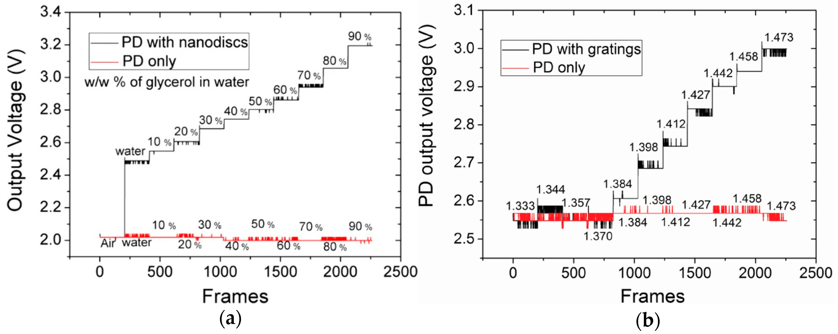
| Shakoor et al. [74,76] | Gold nanodiscs and silicon nitride gratings integrated with CMOS PD | Monolithic | Glycerol and protein | Gold nanodiscs: 270nm /RIU, Silicon nitride gratings: 160 nm/RIU | Gold nanodiscs: 5.6 V/RIU, Silicon nitride gratings: 6.75 V/RIU | 3 × 10⁻³ |
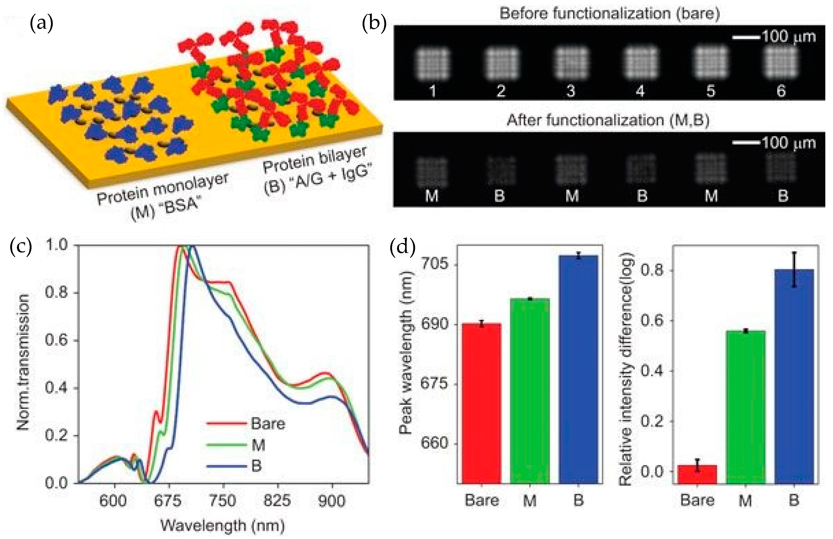
| Cetin et al. [77] | Gold nanohole array readout with CMOS imager | Not monolithic | Protein | 621 nm/RIU | 0.024 relative intensity change of diffraction pattern | 1 µg/mL |
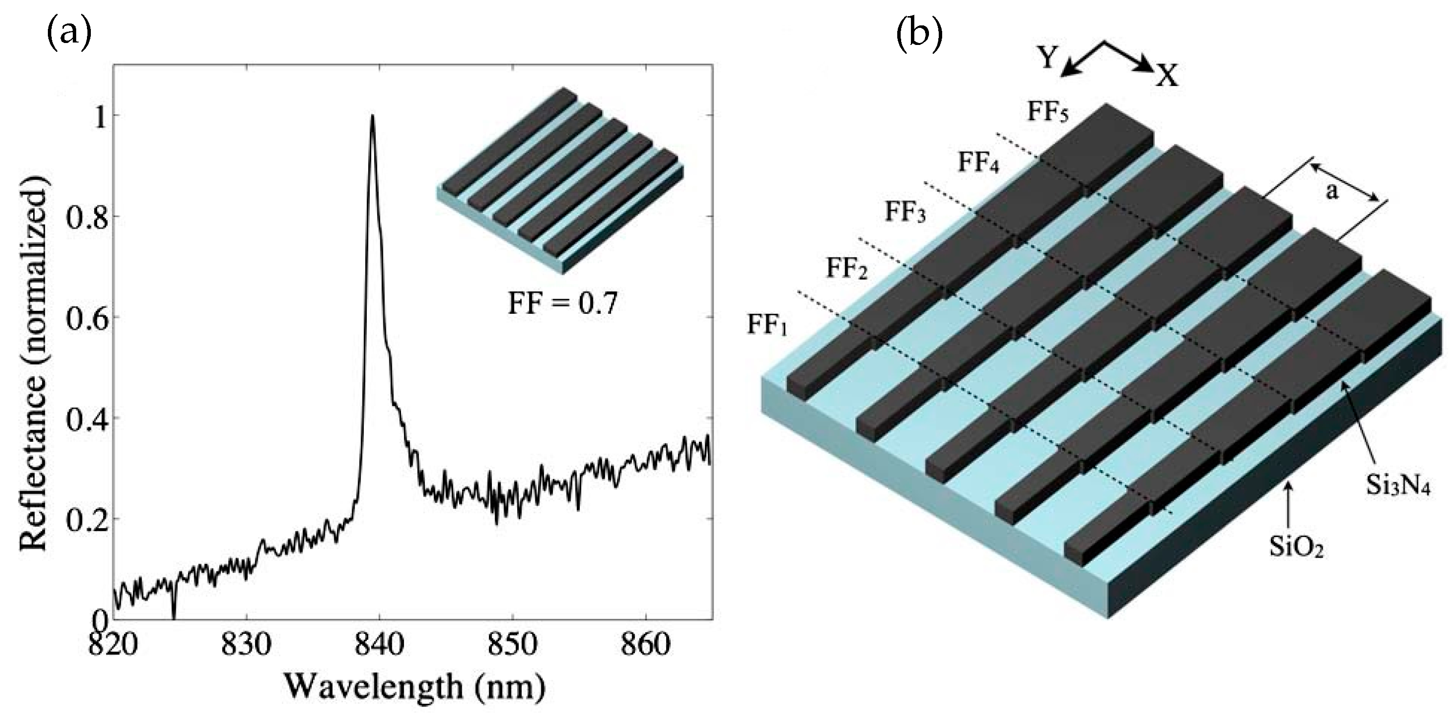
| Triggs et al. [78] | Chirped resonance gratings read by camera | Not monolithic | Glycerol and IgG | 137 nm/RIU | 3469 µm/RIU spatial shift (not wavelength shift) | 2.37 × 10⁻⁴, 40 ng/mL |
© 2019 by the authors. Licensee MDPI, Basel, Switzerland. This article is an open access article distributed under the terms and conditions of the Creative Commons Attribution (CC BY) license (http://creativecommons.org/licenses/by/4.0/).
Share and Cite
Shakoor, A.; Grant, J.; Grande, M.; Cumming, D.R.S. Towards Portable Nanophotonic Sensors. Sensors 2019, 19, 1715. https://doi.org/10.3390/s19071715
Shakoor A, Grant J, Grande M, Cumming DRS. Towards Portable Nanophotonic Sensors. Sensors. 2019; 19(7):1715. https://doi.org/10.3390/s19071715
Chicago/Turabian StyleShakoor, Abdul, James Grant, Marco Grande, and David. R. S. Cumming. 2019. "Towards Portable Nanophotonic Sensors" Sensors 19, no. 7: 1715. https://doi.org/10.3390/s19071715
APA StyleShakoor, A., Grant, J., Grande, M., & Cumming, D. R. S. (2019). Towards Portable Nanophotonic Sensors. Sensors, 19(7), 1715. https://doi.org/10.3390/s19071715