Article

A Compact Thévenin Model for a Rectenna and Its Application to an RF Harvester with MPPT

by
Manel Gasulla
1,*,
Edgar Ripoll-Vercellone
1,2 and
Ferran Reverter
1
1
e-CAT Research Group, Department of Electronic Engineering, Castelldefels School of Telecommunications and Aerospace Engineering, Universitat Politècnica de Catalunya, c/ Esteve Terradas, 7, 08860 Castelldefels (Barcelona), Spain
2
Idneo Technologies, c/ Rec de Dalt s/n., 08100 Mollet del Vallès (Barcelona), Spain
*
Author to whom correspondence should be addressed.
Sensors 2019, 19(7), 1641; https://doi.org/10.3390/s19071641
Submission received: 28 March 2019 / Accepted: 3 April 2019 / Published: 6 April 2019
(This article belongs to the Special Issue Eurosensors 2018 Selected Papers)

Abstract

:
This paper proposes a compact Thévenin model for a rectenna. This model is then applied to design a high-efficiency radio frequency harvester with a maximum power point tracker (MPPT). The rectenna under study consists of an L-matching network and a half-wave rectifier. The derived model is simpler and more compact than those suggested so far in the literature and includes explicit expressions of the Thévenin voltage (Voc) and resistance and of the power efficiency related with the parameters of the rectenna. The rectenna was implemented and characterized from −30 to −10 dBm at 808 MHz. Experimental results agree with the proposed model, showing a linear current–voltage relationship as well as a maximum efficiency at Voc/2, in particular 60% at −10 dBm, which is a remarkable value. An MPPT was also used at the rectenna output in order to automatically work at the maximum efficiency point, with an overall efficiency near 50% at −10 dBm. Further tests were performed using a nearby transmitting antenna for powering a sensor node with a power consumption of 4.2 µW.

1. Introduction

Radio frequency (RF) energy harvesting has been extensively proposed to power tiny devices such as RFID tags, autonomous sensors, or Internet of Things (IoT) nodes. RF energy can be harvested either from dedicated sources, such as in the case of RFID devices [1,2,3,4], or from the RF energy already present in the ambient environment and coming from unintentional sources such as TV, FM radio, cellular, or WiFi emitters [2,5,6,7,8,9,10].
Figure 1 shows the block diagram of an RF harvester powering a sensor node. The rectenna (rectifying antenna) transforms the RF signal to a DC voltage and the maximum power point tracker (MPPT) provides the optimum load to the rectenna to transfer the maximum power to the sensor node.
The rectenna is composed of an antenna, an impedance matching network, and a rectifier. As the available power at the antenna decreases so does the generated voltage. Whenever this voltage is not high enough to properly bias the diodes of the rectifier, power efficiency severely decreases. Several techniques have been proposed to increase the efficiency at low power levels. One of them consists of using an L-matching network for boosting the voltage at the rectifier input [1,3,5,10,11,12,13,14,15,16,17,18,19,20,21]. As for the MPPT, several works propose its use with rectennas using either commercial chips [6,7] or ad hoc designs [22,23,24,25].
With the aim of gaining more insight into the performance of the rectennas, different analytical models are proposed. However, the derived expressions, which in some cases seek to model the rectenna output as an equivalent Thévenin circuit, are rather complex and may require additional simulations or extensive calculations, which hide the influence of the different parameters of the rectenna on its performance [12,18,26,27,28]. At the other extreme, the Thévenin parameters are sometimes inferred by experimental characterization [25,29,30,31,32]. However, in these cases no relationship with the rectenna parameters is established.
Taking into account the previous limitations, this paper proposes a compact Thévenin model for the rectenna with the benefit of achieving manageable expressions of the Thévenin parameters as a function of the parameters of the rectenna so as to gain insight into its operation. In particular, the rectenna under study consists of an L-matching network and of a half-wave rectifier. The proposed model is then experimentally verified and the rectenna further tested in a high-efficency RF harvester with MPPT.
The paper, which continues and expands the work presented in [32], is organized as follows. Section 2 presents the rectenna and the derived Thévenin equivalent. Section 3 describes the MPPT and the sensor node. Section 4 presents the materials and methods and Section 5 provides the experimental results and discussions. Finally, Section 6 concludes the work. Complementarily, two appendices are included. Appendix A presents an analytical development useful for the derivation of the Thévenin equivalent and Appendix B shows simulations of the rectenna with and without the matching network.

2. Rectenna and Its Thévenin Model

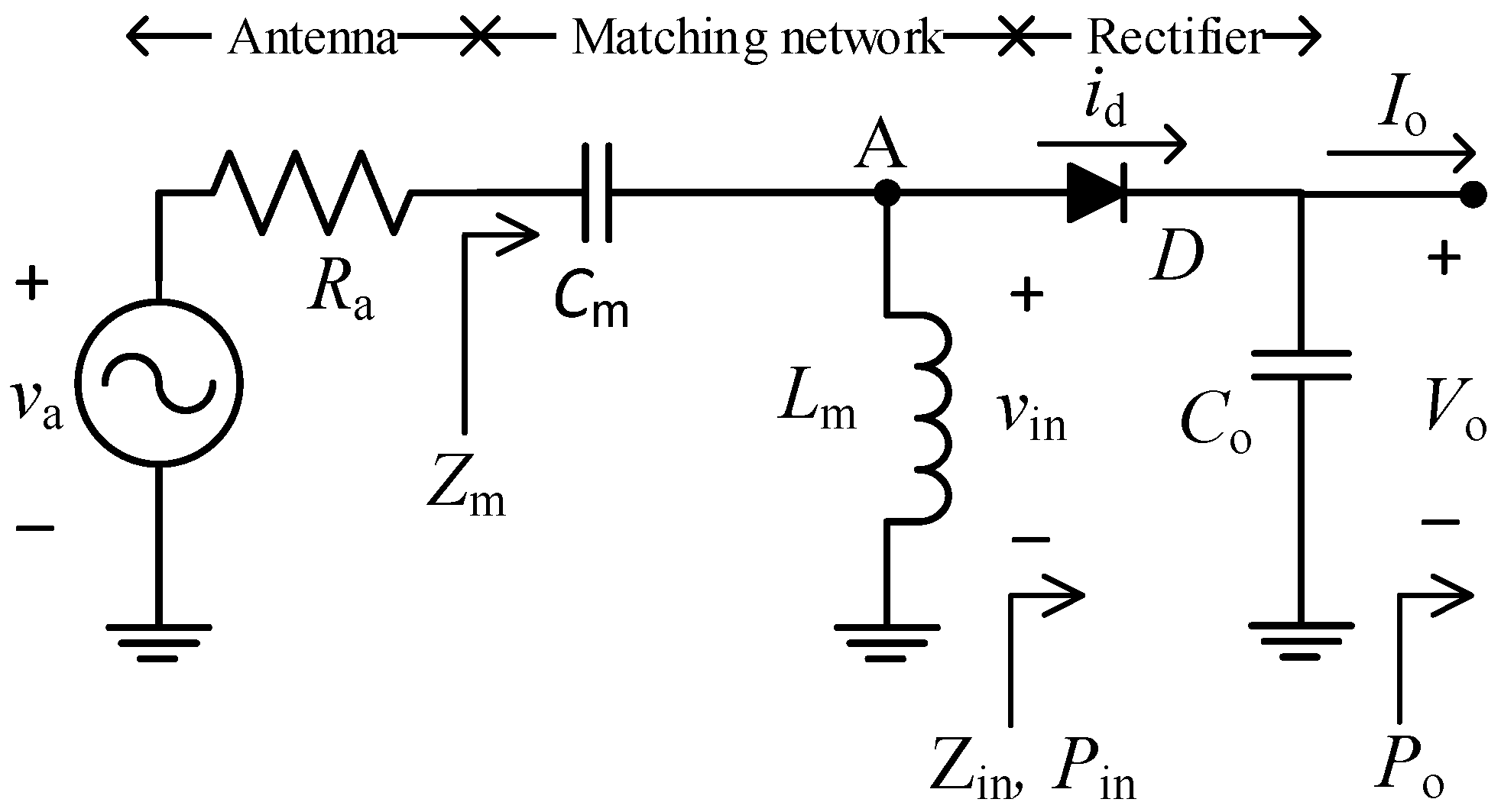
Figure 2 shows the schematic circuit of the rectenna under study [33], which includes a high-pass L-matching network (composed of a capacitor Cm and an inductor Lm), a half-wave rectifier, and an output filtering capacitor (Co). The antenna is modelled by a sinusoidal voltage source va of amplitude Vap and frequency fo with a series radiation resistance Ra. On the other hand, vin, Zin, and Pin are, respectively, the sinusoidal voltage, impedance, and power at the input of the rectifier, id is the diode current, and Vo, Io, and Po are, respectively, the DC voltage, current, and power at the rectenna output. An equivalent resistance Ro is defined as Vo/Io.
The amplitude Vap is given by [12] as follows:
V ap = 2 2 R a P av ,
where Pav is the available power at the antenna. The matching network, at matching conditions, that is, Zm = Ra (where Zm is defined in Figure 2), boosts the voltage at the input of the rectifier by a voltage gain, Gt, given by [33] as follows:
G t = V inp V ap = 1 2 ( 1 + Q 2 ) ,
where Vinp is the voltage amplitude of vin and Q is the circuit quality factor given by:
Q = 1 ω o C m R a ,
where ωo = 2πfo. On the other hand, the value of Lm must comply:
L m = 1 ω o 2 1 C p + C m Q 2 / ( 1 + Q 2 ) ,
where Cp models the parasitic capacitance between node A and ground.
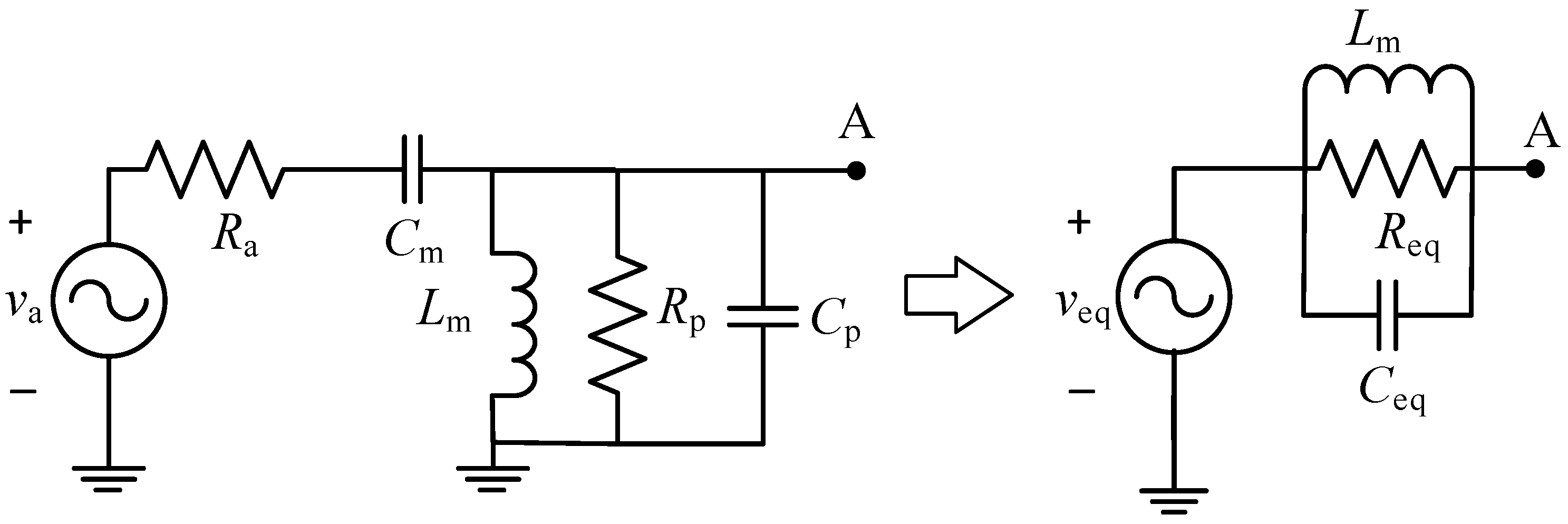
To ease the analysis of the proposed rectenna and also gain more insight into its performance, a compact Thévenin model is provided here. First, the left-hand equivalent circuit of Figure 3 accounts for the antenna, the matching network, and the parasitic elements (Rp-Cp) of the coil, diode, and layout of the circuit. These parasitic elements are derived in Appendix A, where Rp models the losses of the coil and diode and Cp includes the parasitic capacitance of the diode, coil, and layout.
Analyzing the left-hand circuit of Figure 3 at fo, we can achieve the Thévenin equivalent represented by the right-hand circuit of Figure 3, where:
v eq = 2 G t v a R p 4 G t 2 R a + R p , R eq = ( 4 G t 2 R a ) R p , C eq = C m Q 2 1 + Q 2 + C p .
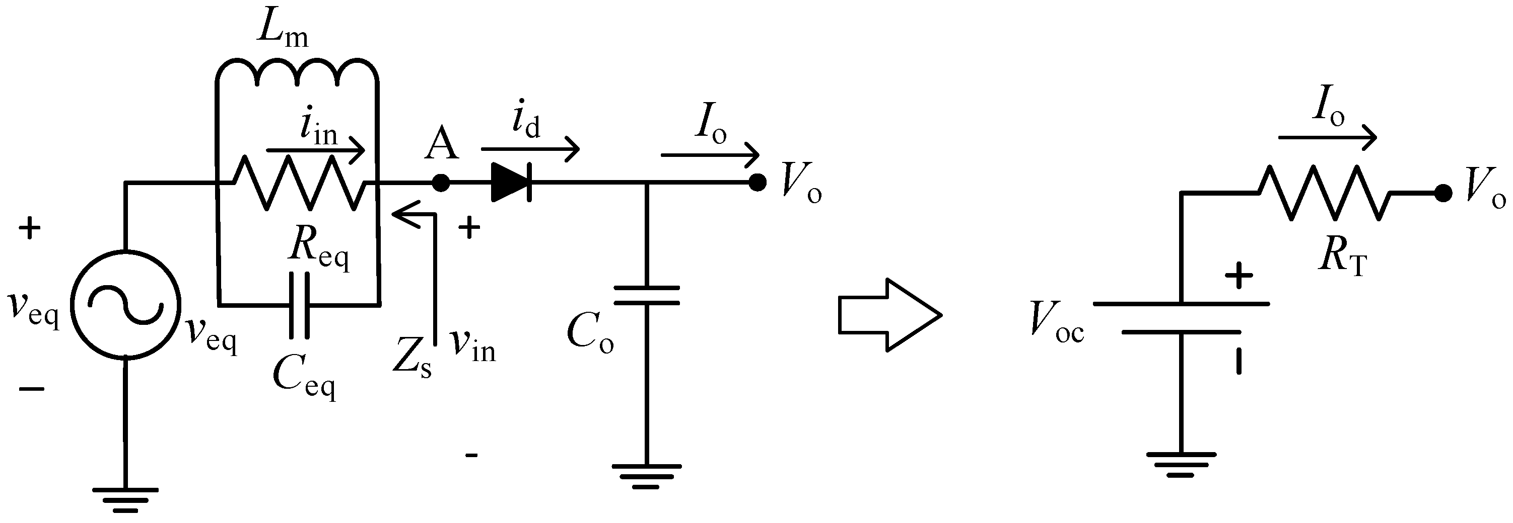
Next, the Thévenin equivalent of Figure 3 is linked to the next stage of the rectenna, the rectifier, resulting in the left-hand circuit of Figure 4, where the diode does not include its parasitic elements since they have been already considered in the previous derivation (they are included in Req and Ceq). The diode is forward biased when vin, assumed sinusoidal, surpasses Vo. As a result, id is pulsed and is composed of the fundamental frequency (fo) as well as its harmonics and a DC component (Io). Impedance Zs (defined in the circuit) is zero at DC (due to the coil Lm) and is equal to Req at fo since Lm and Ceq form a parallel resonant circuit presenting an infinite impedance. On the other hand, at the harmonics of fo we have Zs << Req (due to Ceq) whenever Q is high enough. Therefore, only the current at fo (iin) originates a voltage drop and vin will be sinusoidal, as assumed before. Thus, apart from boosting the voltage, the matching network ideally acts as an input band-pass filter that prevents any of the DC current and harmonics to flow through the antenna resistance and dissipate power. This leads to an ideal rectenna efficiency of 100%, assuming no losses in the circuit components and in the diode [34]. Contrariwise, when no matching network is present, maximum rectenna efficiency decreases to 46%, due to the additional losses at Ra originated by the current harmonics generated by the diode pulsed current, as demonstrated in [35]. Appendix B confirms these results via simulations. Finally, the value of Co has to be much higher than the diode junction capacitance (Cj), as explained in Appendix A, to keep Vo nearly constant, that is, with a low voltage ripple (ΔVo). This second condition leads to:
C o > I o Δ V o f o .
The left-hand circuit of Figure 4 leads to the equivalent Thévenin circuit of the rectenna, represented by the right-hand circuit of Figure 4, by linking their output voltage–current relationship. For the left-hand circuit, we have:
V o = V inp V γ ,
assuming a fixed forward voltage drop Vγ at the diode and:
V inp = V eqp R eq I inp ,
where Veqp and Iinp are the amplitudes of veq and iin, respectively. Substituting (8) into (7) provides:
V o = V eqp V γ R eq I inp .
On the other hand, for the right-hand circuit we have:
V o = V oc R T I o .
Then, by equating powers, we obtain:
P in = P o + P d ,
where
P in = V inp I inp 2 , P o = V o I o , P d = V γ I o ,
and Pd is the average power dissipated across the diode. Thus, replacing (12) into (11) and using (7), we arrive at the following:
I inp = 2 I o .
Finally, using (13) in (9) and equating (9) and (10), we obtain the parameters of the Thévenin model:
V oc = V eqp V γ , R T = 2 R eq ,
where Veqp can be derived from veq in (5), using Vap instead of va, resulting in:
V eqp = 2 G t V ap R p 4 G t 2 R a + R p .
Then, using (15) and Req of (5) in (14), we have:
V oc = 2 G t V ap R p 4 G t 2 R a + R p V γ , R T = 2 [ ( 4 G t 2 R a ) R p ] .
Therefore, from (16), with an increasing Pav and thus Vap, Voc increases whereas RT holds constant. Next, from (10), we can express Io as:
I o = ( V oc V o ) / R T ,
and the output power Po over a load resistor Ro can be simply calculated as:
P o = V o I o = V oc V o V o 2 R T ,
being the power efficiency of the rectenna as:
η rect = P o P av = V oc V o V o 2 P av R T .
Applying the maximum power transfer theorem, maximum power is extracted from the rectenna for Vo = 0.5Voc, which is known as the maximum power point (MPP) voltage (VMPP). From (19), the resulting efficiency is as:
η rect , max = V oc 2 4 P av R T .
Thus, using (16) in (20), we arrive at:
η rect , max = R p 4 G t 2 R a + R p ( 1 V γ 2 R a P av 4 G t 2 R a + R p 4 G t R p ) 2 .
As can be seen from (21), ηrect,max increases with increasing Pav. Obviously, with no losses (Rp = ∞ and Vγ = 0) ηrect,max = 1 is obtained. On the other hand, the dependence of ηrect,max on Gt is rather more complex. In [33], an optimum value of Gt was derived arising from the trade-off between the losses introduced by the coil and that due to the voltage drop of the diode. This optimum gain leads, from (16), to a particular value of RT.

3. MPPT and Sensor Node

In general, a sensor node directly connected to the output of the rectenna will not provide an equivalent resistance Ro = RT, at which the rectenna output operates at the MPP. Thus, an impedance matching stage (in addition to the matching network of the rectenna) is needed between the rectenna output and the sensor node, which can be implemented by a DC/DC converter. An MPPT, which consists of a DC/DC converter plus a tracking algorithm, can be used for automatically searching and settling that optimum value of Ro, which also corresponds to Vo = VMPP. Thus, the overall power efficiency of the RF harvester will be given by the following:
η T = η rect , max η MPPT ,
where ηMPPT is the efficiency of the MPPT and ηrect = ηrect,max since the MPPT biases the rectenna at the MPP.
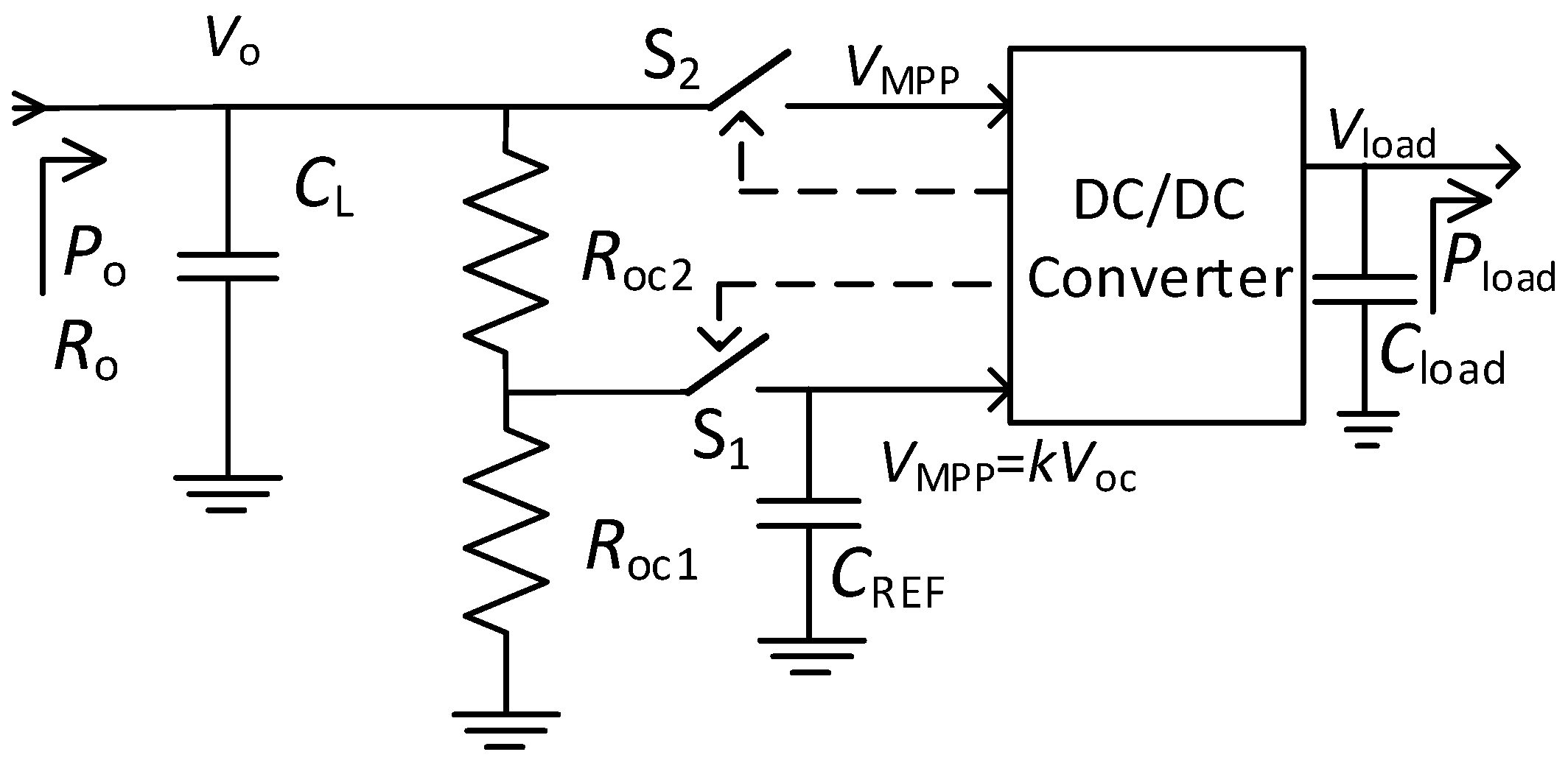
In this work, the fractional open circuit voltage (FOCV) MPPT technique is used, since it leads to simple and power efficient implementations. In this technique, the open circuit voltage (Voc) of the energy transducer (a rectenna here) is first measured and a fraction k of Voc is used to operate at VMPP and thus achieve ηrect,max. Taking into account the analysis in Section 2, a proper choice here is k = 0.5 (Vo = VMPP = 0.5Voc).
Figure 5 presents the block diagram for the implementation of the FOCV MPPT technique, where CL, CREF, and Cload are capacitors, Roc1 and Roc2 are resistors, S1 and S2 are switches, Vload is the output voltage used to power the sensor node, and Pload is the power transferred to the sensor node. The operation is the following. First, S1 closes and S2 opens (sampling period). For high values of Roc1 and Roc2, the output of the rectenna can be considered as open and thus Vo = Voc. The voltage divider formed by Roc1 and Roc2 fixes VMPP = kVoc, being k = 0.5 here (i.e., Roc1 = Roc2). The input capacitor (CL) momentarily stores the incoming harvested energy. Secondly, S1 opens and S2 closes (regulation period). Thus, VMPP holds constant thanks to CREF, and the DC/DC converter settles Vo around VMPP and transfers the harvested energy by the rectenna to the sensor node.
In order to periodically update Voc (i.e., a change in Pav changes Voc), the described sequence is periodically repeated, with the sampling period being much shorter than the regulation period. In this way, Vo will settle most of time at VMPP. To increase the efficiency at light loads, the DC/DC converter uses special control techniques such as pulse frequency modulation (PFM) or burst-mode [36].
Taking into account (22), Pload can be related with Pav as follows:
P load = η T P av .
The value of Pload and thus of Pav must be enough, in average, to power the sensor node, which usually includes a rechargeable storage unit. This unit accounts for the variability of Pav, gathering or providing energy whenever Pav is higher or lower than required. Storage units can be supercapacitors, batteries, or a combination of both [37]. On the other hand, the required value of Pload and thus of Pav can be reduced by operating the sensor node in sleep mode most of the time and minimizing its active time.

4. Materials and Methods

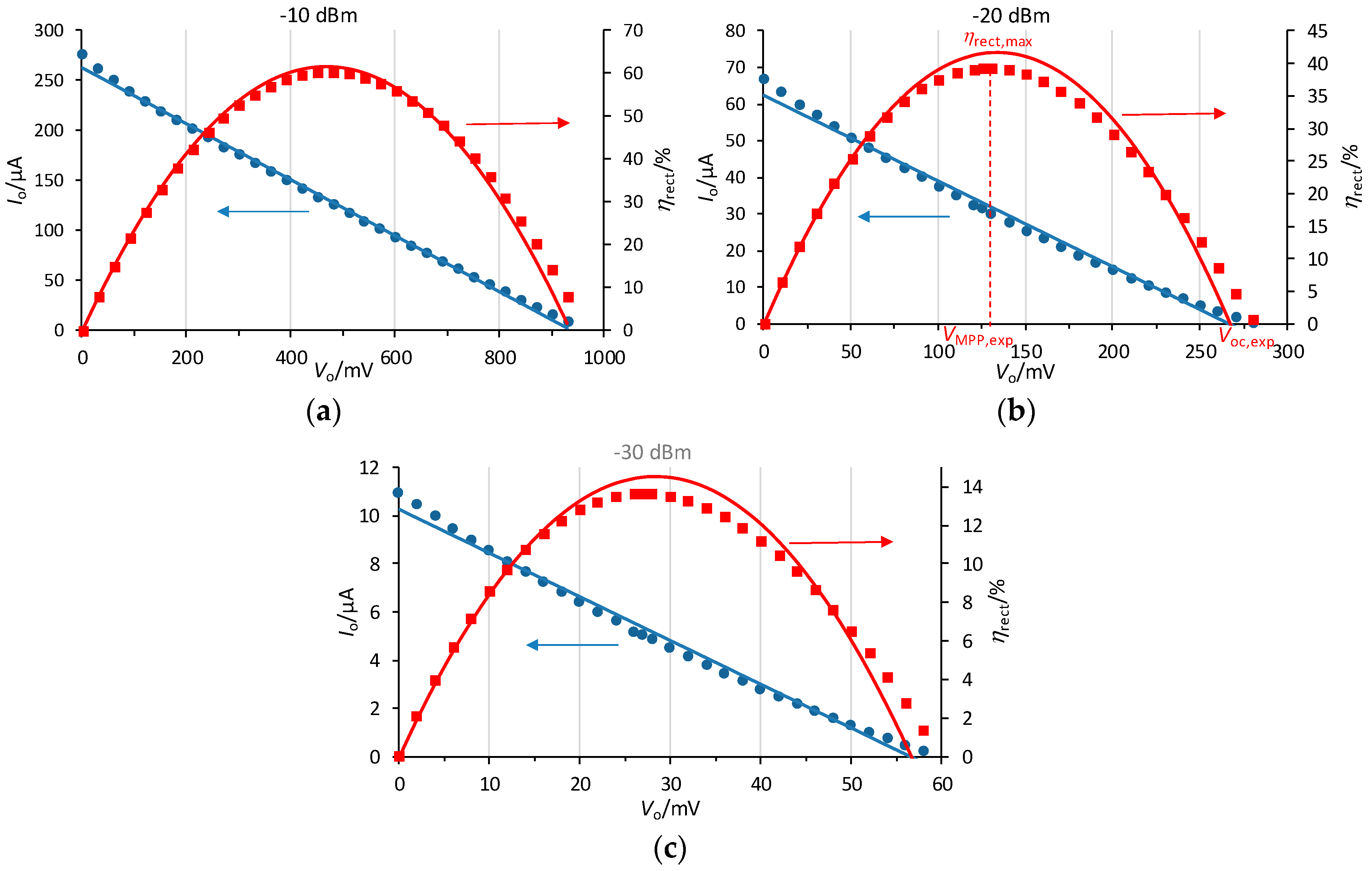
The rectenna shown in Figure 2 was implemented on a printed circuit board with Rogers substrate and with the following components: Cm = 0.5 pF (AVX, Fountain Inn, SC, USA), Lm = 27 nH (0603CS model, Coilcraft, Cary, IL, USA), Co = 1 nF, and a Schottky HSMS-2850 diode (Avago Technologies, San Jose, CA, USA) [33]. The selected value of Co comfortably accomplished, in order to theoretically have a small ripple (below 1 mV) with the values of Io shown later in Section 5, as well as the condition stated in Appendix A (Co >> Cj). The circuit of Figure 2 was used for the rectenna characterization, where an RF generator (Agilent E4433B, Santa Clara, CA, USA) was connected at the input instead of the antenna and a Source Measure Unit (SMU, Agilent B2901A, Santa Clara, CA, USA) configured as a voltage sink (quadrant IV) at the output. The generator was set at a tuned optimal frequency of 808 MHz and at different values of Pav (−30 dBm, −20 dBm, and −10 dBm). For each value of Pav, the SMU was set at different values of Vo while measuring Po. Then, ηrect was obtained as Po/Pav.
As for the FOCV MPPT, a BQ25504 chip (Texas Instruments, Dallas, TX, USA) was used, and in particular an evaluation board provided by the manufacturer. The chip contains a boost converter with PFM control and the board includes, in reference to Figure 5, CL = 4.8 µF (combination of two ceramic capacitors of 4.7 μF and 100 nF placed in parallel), CREF = 10 nF, and Cload = 104.8 µF (combination of three ceramic capacitors of 100 μF, 4.7 μF, and 100 nF placed in parallel). The default values of Roc1 and Roc2 were modified to 10 MΩ in order to fix k = 0.5 (the default value is set to 0.78). The sampling and regulation periods are prefixed by the chip to 256 ms and 16 s, respectively. Then, the efficiency of the whole RF harvester (rectenna plus MPPT) was characterized by using the RF generator at the input of the rectenna and the SMU set at 3 V at the output of the MPPT (Vload). The RF generator was set at different values of Pav, from −20 dBm to −5 dBm in steps of 1 dBm, and for each value the SMU measured the output power Pload. Then, from (23), ηT was estimated.
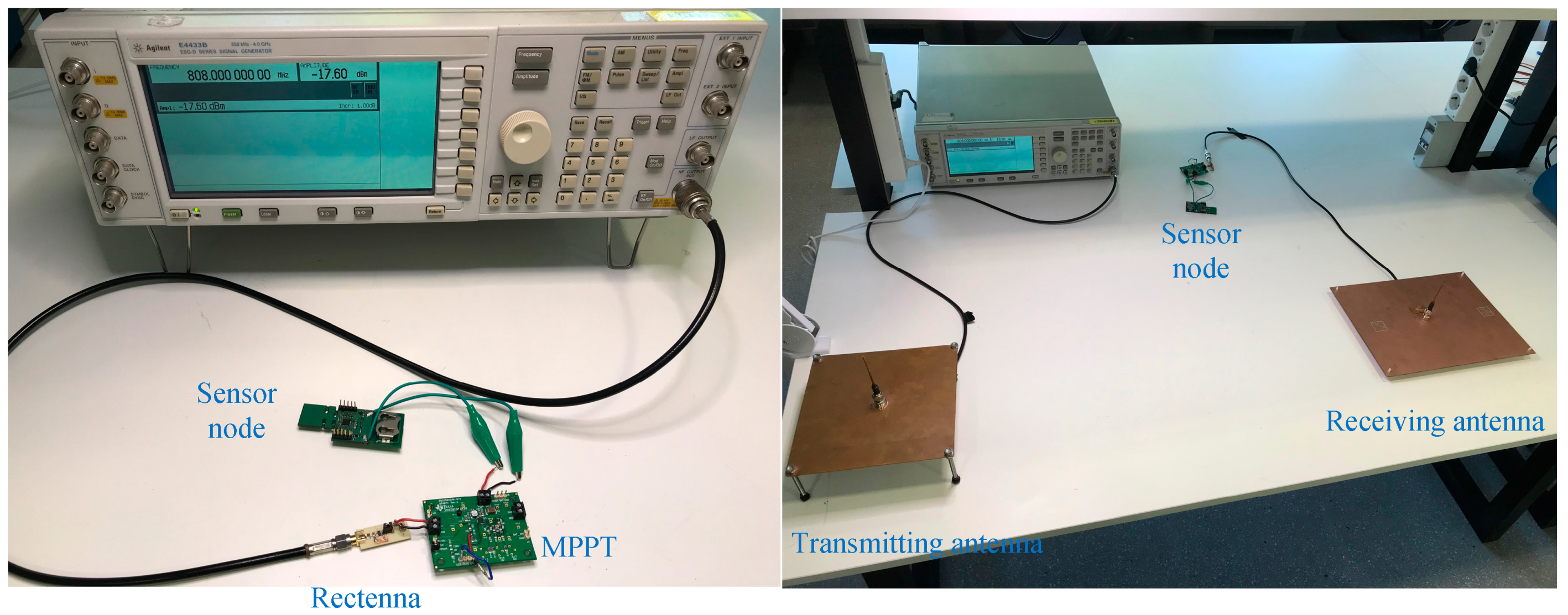
For demonstration purposes, the RF harvester including the MPPT was also employed to power a sensor node intended to upgrade a mechanical gas meter to a smart device [38]. For these tests, the node was programmed to stay in a standby mode, consuming 1.4 µA. The input power (Pav) was set to keep the voltage supply of the sensor node (Vload) at 3 V, thus Pload = 4.2 µW. As for the RF harvester input, two configurations were used: (1) an RF generator and (2) a receiving monopole antenna. In the second case, another identical monopole antenna was connected to a nearby RF generator, jointly acting as a wireless energy transmitter. The antennas showed an insertion loss higher than 10 dB at 808 MHz. Figure 6 shows pictures of both setups.

5. Experimental Results and Discussion

As for the proposed rectenna, Figure 7 shows the measured values (in dots) of Io (blue circles) and ηrect (red squares) as a function of Vo at different values of Pav. A least-squares fitting of (17) to the experimental data of Io was performed (blue continuous line) to obtain the Thévenin parameters (Voc and RT) at each power level, which are shown in Table 1. Calculated values of Vap, from (1), and of Veqp, from (15), are also included in Table 1. This fitting differs from that performed in [32], where the efficiency data (ηrect) were used instead, which leads to slight differences in the Thévenin parameters. The new fitting procedure was considered more convenient as both Voc and RT can be more easily inferred from the fitting curve. As can be seen, the fitting curves match well the experimental data, and more at the highest power of −10 dBm, which confirms that the rectenna can be well approximated by a Thévenin equivalent circuit. Then, Voc and RT were used to obtain ηrect using (19), and the resulting curves are also represented in Figure 7 (red continuous line). The match with the experimental data is good, and again better at −10 dBm.
With Cm = 0.5 pF, Ra = 50 Ω, and fo = 808 MHz, Q = 7.88 results from (3), and Gt = 3.97 from (2). Then, from (16) and assuming the value of Rp = 9.21 kΩ derived in Appendix A, RT = 4.7 kΩ is obtained, which is within the range of values found in Table 1. The inferred values of RT moderately change with Pav due to the relative low value of Q, which limits the accuracy of the rectenna model proposed in Section 2. However, a higher value of Q, which could be obtained using a lower value of Cm and appropriately readjusting Lm, does not lead to the optimum gain Gt [33], thus decreasing the power efficiency. On the other hand, Voc in Table 1 increases with increasing Pav and thus Vap, which agrees with (16). The values of Voc can be estimated in advance, when necessary, from (16) by calculating Veqp from (15), shown in Table 1, and inferring a value of Vγ from the manufacturer data or from simulations.
From the measured data of ηrect (red squares in Figure 7), Table 2 shows the achieved ηrect,max and its corresponding voltage (VMPP,exp), as well as the experimental open circuit voltage (Voc,exp) of the rectenna. In Figure 7, ηrect,max, VMPP,exp, and Voc,exp are also marked for Pav = −20 dBm. As can be seen, ηrect,max increases with increasing Pav, ranging from 13.6% at −30 dBm to 60.3% at −10 dBm, which agrees with (21). The values of ηrect,max can be estimated in advance, when necessary, from (21) and inferring a value of Vγ from the manufacturer data or from simulations. One particular case is the upper limit, which would be achieved for Pav→∞ (or Vγ→0), in our case 74%. The resulting efficiencies (ηrect,max) are among the highest published in the literature for similar designs [33]. On the other hand, Voc from Table 1 nearly matches Voc,exp. Finally, VMPP,exp equates or nearly matches 0.5 Voc,exp, the regulated voltage at the input of the MPPT. Thus, the proposed and implemented MPPT will be able to extract the maximum power (or nearly) from the rectenna.
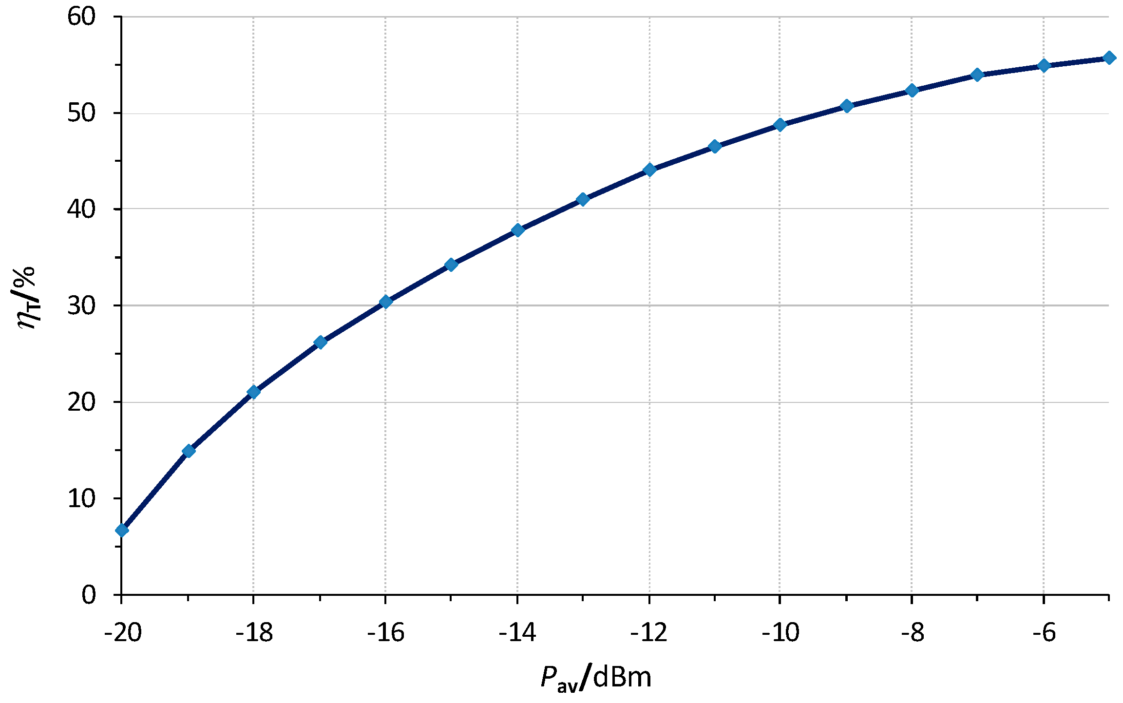
As for the whole RF harvester (rectenna plus the MPPT), Figure 8 shows the experimental values of ηT versus Pav. At −20 dBm, ηrect,max = 39.3% (Table 2) but ηT = 6.5%, resulting, from (22), in ηMPPT = 16.5%. This low value of ηMPPT is due to both a low input voltage value (140 mV = 0.5 Voc,exp) and a low value of Po (3.9 µW = ηrect,maxPav). Contrariwise, at −10 dBm, ηrect,max = 60.3% and ηT = 48.6%, resulting in ηMPPT = 80.6%, which agrees with the data from the BQ25504 chip’s datasheet. At higher values of Pav (−5 dBm), ηT reached a value of 55.6%. Compared to [6], where a similar chip for the MPPT was used, ηT is quite higher.
When powering the sensor node, the required value of Pav was −17.6 dBm. This value fits well with (23), considering the corresponding efficiency in Figure 8 (≈24%). This performance was also tested with the antennas at a distance of 0.5 and 1 m. The power output of the remote RF generator was tuned at appropriate values so as to operate the node, resulting in 8.0 and 13.2 dBm, respectively. These values accounted for the respective link budgets.

6. Conclusions

This work proposed a compact Thévenin model for a rectenna and its application for designing a high-efficiency RF harvester. The rectenna under study consists of an L-matching network and a half-wave rectifier. Explicit expressions for the Thévenin voltage and resistance were derived that offer insight into the operation of the rectenna. An expression was also provided for the power efficiency. The rectenna was implemented and characterized from −30 to −10 dBm at 808 MHz and the results mainly agreed with the derived model, with differences arising from the limited Q factor of the matching network. High efficiencies were obtained, in particular 60% at −10 dBm. Then, an ensuing MPPT was also added, where the behavior of the rectenna as an equivalent Thévenin circuit allowed the use of a simple FOCV technique. The whole RF harvester (rectenna plus MPPT) showed an overall efficiency near 50% at −10 dBm. Further tests were performed with a nearby transmitting antenna for powering a sensor node with a power consumption of 4.2 µW.

Author Contributions

Conceptualization, M.G.; Formal analysis, M.G. and F.R.; Funding acquisition, M.G. and F.R.; Investigation, M.G. and E.R.-V.; Methodology, M.G.; Project administration, M.G. and F.R.; Writing–original draft, M.G.; Writing–review and editing, M.G. and F.R.

Funding

This work was supported by the Secretariat of University and Research of the Ministry of Business and Knowledge of the Government of Catalonia, by the Spanish State Research Agency (AEI) and by the European Regional Development Fund under Project TEC2016-76991-P.

Acknowledgments

The authors wish to thank Josep Jordana, Francesc-Josep Robert, and Jordi Berenguer for their initial support, and the Castelldefels School of Telecommunications and Aerospace Engineering, Barcelona, Spain, for the RF instrumentation needed to perform the experiments.

Conflicts of Interest

The authors declare no conflict of interest.

Appendix A. Parallel Circuit Model of the Inductor and Diode
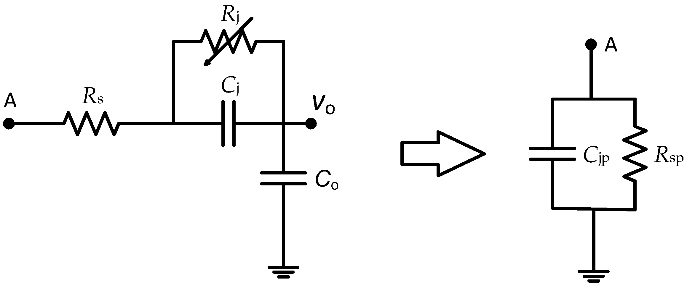
The use of a matching network leads to sinusoidal voltage and current waveforms at fo, as mentioned in Section 2. Here, the equivalent circuit model at fo is derived from the manufacturer models of the diode (https://docs.broadcom.com/docs/AV02-1377EN) and inductor (https://www.coilcraft.com/pdfs/spice_0603cs.pdf) used for the implemented rectenna and reported in Section 4. This model will be used in the left-hand circuit of Figure 3.
First, the left-hand circuit in Figure A1 shows the equivalent linear circuit model of the diode, connected between node A and the Vo node at Figure 2, together with the output capacitor Co, where Rs is the parasitic series resistance, Cj is the parasitic junction capacitance, and Rj is the junction resistance. Rj depends inversely on the bias current and makes only sense for modelling small current variations around a bias current. In our case, the diode current is pulsed and thus the inclusion of Rj is not appropriate. Instead, a constant voltage drop will be assumed in Section 2 for the analysis of the circuit of Figure 4.
Figure A1. Equivalent linear circuit model of the HSMS-2850 diode together with (left) the output capacitor Co and (right) its parallel equivalent circuit.
Sensors 19 01641 g0a1
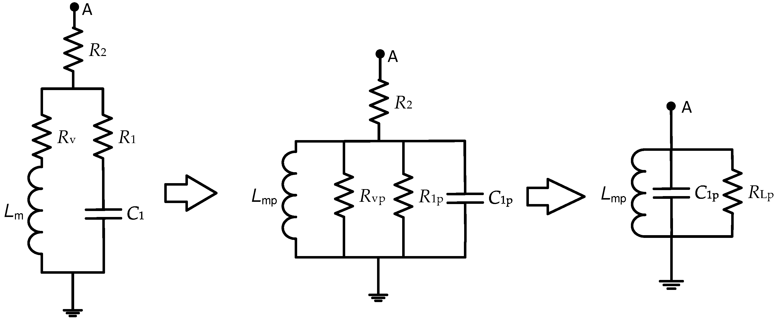
Using the series-to-parallel equivalent circuit transformation for the left-hand circuit of Figure A1 without Rj and considering Co >> Cj, the right-hand circuit results, where:
R sp = R s R s 2 C j 2 ω o 2 + 1 R s 2 C j 2 ω o 2 ,
C jp = C j R s 2 C j 2 ω o 2 + 1 .
From the diode datasheet, Rs = 25 Ω and Cjo = 0.18 pF (Cjo is Cj at zero bias and will be the assumed value for Cj hereafter). With fo = 808 MHz, Rsp = 47.9 kΩ results from (A1) and CjpCj = 180 fF results from (A2).
As for the inductor, connected between node A and ground at Figure 2, the left-hand circuit of Figure A2 shows the manufacturer model, where R v = k f o . Using the series-to-parallel circuit transformation, the circuit in the middle is obtained, where:
L mp = L m [ 1 + ( R v ω o L m ) 2 ] .
R vp = R v [ 1 + ( ω o L m R v ) 2 ] ,
R 1 p = R 1 R 1 2 C 1 2 ω o 2 + 1 R 1 2 C 1 2 ω o 2 ,
C 1 p = C 1 R 1 2 C 1 2 ω o 2 + 1 .
From the coil datasheet, R1 = 17 Ω, R2 = 30 mΩ, C1 = 49 fF, Lm = 27 nH, and k = 5.75 × 10⁻⁵. At 808 MHz, Rv = 1.63 Ω and from (A3) to (A6), LmpLm = 27 nH, Rvp = 11.5 kΩ, R1p = 950 kΩ, and C1pC1 = 49 fF. Then, neglecting R2, since it is very small, the right-hand circuit of Figure A2 is obtained, where R Lp = R vp R 1 p = 11.4   k Ω .
Figure A2. (left) Manufacturer model of the inductor and (middle and right) equivalent circuits.
Sensors 19 01641 g0a2
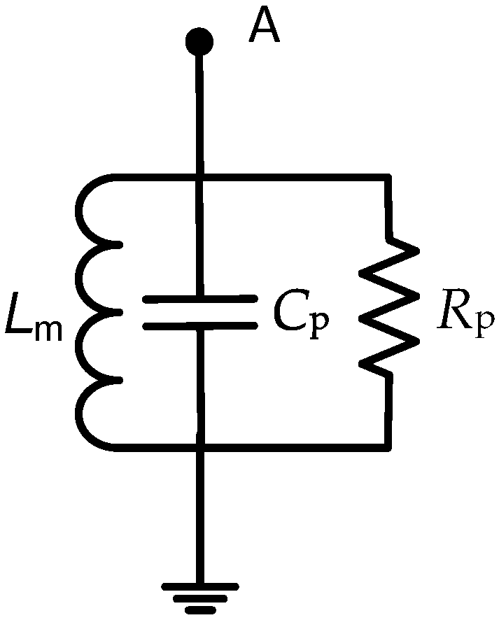
Joining the right-hand circuits in Figure A1 and Figure A2, and considering the parasitic capacitance from node A to ground arising from the layout (Clay), the circuit in Figure A3 is obtained, where:
R p = R sp R Lp = 9.21   k Ω ,
C p = C jp + C 1 p + C lay .
Figure A3. Parallel equivalent circuit of the inductor.
Sensors 19 01641 g0a3
This equivalent circuit is used in the left-hand circuit of Figure 3.

Appendix B. Simulations of the Rectenna Efficiency with and without an L-Matching Network

In order to highlight the benefits of using a matching network, we report simulation results of the rectenna efficiency with and without an L-matching network. For the simulations, the ADS software (Version 2017, Keysight, Santa Rosa, CA, USA) was used. The simulated circuit with the matching network was that of Figure 2 with a resistor Ro connected at its output, in parallel with Co. Ideal components were used for the matching network with the values reported in Section 4. The diode was modelled without parasitic elements (null series resistance and junction capacitance) but with a saturation current of 3 µA (that corresponding to the HSMS-2850 diode used for the implemented rectenna). For the RF source, a frequency of 808 MHz (that used for the experiments) was used with Pav ranging from −10 to 50 dBm in steps of 20 dB. For the circuit without the matching network, the right terminal of Ra was directly connected to the diode anode (node A). For both circuits, a harmonic balance analysis was performed with Pav and Ro as sweeping parameters.
Figure A4 shows the simulation results of the rectenna efficiency (ηrect = Po/Pav) plotted against Ro for different values of Pav. The left graph shows the results for the circuit with the L-matching network. As can be seen, ηrect steeply increases for increasing values of Pav, achieving around 99% at Pav = 50 dBm. At −10 dBm, efficiency is higher than the corresponding results of Figure 7 because ideal components were used for the simulation. On the other hand, the right graph shows the results for the circuit without the L-matching network. As can be seen, ηrect steeply increases for increasing values of Pav but now reaches a maximum value around 46%, as predicted theoretically in [35], due to the additional losses at Ra originated by the current harmonics generated by the diode pulsed current. At −10 dBm, efficiency is lower than 4%. Therefore, the use of the matching network allows a notable increase in the rectenna efficiency, because it provides voltage gain and prevents any of the DC current and harmonics to flow through the antenna resistance.
Figure A4. Rectenna efficiency for the circuit (left) with and (right) without the matching network.
Sensors 19 01641 g0a4

References

  1. Shameli, A.; Safarian, A.; Rofougaran, A.; Rofougaran, M.; De Flaviis, F. Power Harvester Design for Passive UHF RFID Tag Using a Voltage Boosting Technique. IEEE Trans. Microw. Theory Tech. 2007, 55, 1089–1097. [Google Scholar] [CrossRef]
  2. Sample, A.; Smith, J.R. Experimental results with two wireless power transfer systems. In Proceedings of the 2009 IEEE Radio and Wireless Symposium, San Diego, CA, USA, 18–22 January 2009; pp. 16–18. [Google Scholar]
  3. Attaran, A.; Rashidzadeh, R.; Muscedere, R. Chipless RFID tag using RF MEMS switch. Electron. Lett. 2014, 50, 1720–1722. [Google Scholar] [CrossRef]
  4. Álvarez López, Y.; Franssen, J.; Álvarez Narciandi, G.; Pagnozzi, J.; González-Pinto Arrillaga, I.; Las-Heras Andrés, F. RFID Technology for Management and Tracking: E-Health Applications. Sensors 2018, 18, 2663. [Google Scholar] [CrossRef] [PubMed]
  5. Singh, G.; Ponnaganti, R.; Prabhakar, T.V.; Vinoy, K.J. A tuned rectifier for RF energy harvesting from ambient radiations. AEU-Int. J. Electron. Commun. 2013, 67, 564–569. [Google Scholar] [CrossRef]
  6. Talla, V.; Kellogg, B.; Ransford, B.; Naderiparizi, S.; Gollakota, S.; Smith, J.R. Powering the Next Billion Devices with Wi-Fi. In Proceedings of the 11th ACM Conference on Emerging Networking Experiments and Technologies, Heidelberg, Germany, 1–4 December 2015. [Google Scholar]
  7. Piñuela, M.; Mitcheson, P.D.; Lucyszyn, S. Ambient RF energy harvesting in urban and semi-urban environments. IEEE Trans. Microw. Theory Tech. 2013, 61, 2715–2726. [Google Scholar] [CrossRef]
  8. Di Marco, P.; Stornelli, V.; Ferri, G.; Pantoli, L.; Leoni, A. Dual band harvester architecture for autonomous remote sensors. Sens. Actuators A Phys. 2016, 247, 598–603. [Google Scholar] [CrossRef]
  9. Shaker, G.; Chen, R.; Milligan, B.; Qu, T. Ambient electromagnetic energy harvesting system for on-body sensors. Electron. Lett. 2016, 52, 1834–1836. [Google Scholar] [CrossRef]
  10. Stoopman, M.; Keyrouz, S.; Visser, H.J.; Philips, K.; Serdijn, W.A. Co-design of a CMOS rectifier and small loop antenna for highly sensitive RF energy harvesters. IEEE J. Solid-State Circuits 2014, 49, 622–634. [Google Scholar] [CrossRef]
  11. Soltani, N.; Yuan, F. A High-Gain Power-Matching Technique for Efficient Radio-Frequency Power Harvest of Passive Wireless Microsystems. IEEE Trans. Circuits Syst. I Regul. Pap. 2010, 57, 2685–2695. [Google Scholar] [CrossRef]
  12. Curty, J.-P.; Joehl, N.; Krummenacher, F.; Dehollain, C.; Declercq, M.J. A model for u-power rectifier analysis and design. IEEE Trans. Circuits Syst. I Regul. Pap. 2005, 52, 2771–2779. [Google Scholar] [CrossRef]
  13. Jordana, J.; Reverter, F.; Gasulla, M. Power Efficiency Maximization of an RF Energy Harvester by Fine-tuning an L-matching Network and the Load. Procedia Eng. 2015, 120, 655–658. [Google Scholar] [CrossRef] [Green Version]
  14. Abouzied, M.A.; Ravichandran, K.; Sanchez-Sinencio, E. A Fully Integrated Reconfigurable Self-Startup RF Energy-Harvesting System With Storage Capability. IEEE J. Solid-State Circuits 2017, 52, 704–719. [Google Scholar] [CrossRef]
  15. Nimo, A.; Grgić, D.; Reindl, L.M. Optimization of Passive Low Power Wireless Electromagnetic Energy Harvesters. Sensors 2012, 12, 13636–13663. [Google Scholar] [CrossRef] [Green Version]
  16. Chaour, I.; Fakhfakh, A.; Kanoun, O. Enhanced Passive RF-DC Converter Circuit Efficiency for Low RF Energy Harvesting. Sensors 2017, 17, 546. [Google Scholar] [CrossRef] [PubMed]
  17. Scorcioni, S.; Larcher, L.; Bertacchini, A. Optimized CMOS RF-DC converters for remote wireless powering of RFID applications. In Proceedings of the 2012 IEEE International Conference on RFID (RFID), Orlando, FL, USA, 3–5 April 2012; pp. 47–53. [Google Scholar]
  18. De Carli, L.G.; Juppa, Y.; Cardoso, A.J.; Galup-Montoro, C.; Schneider, M.C. Maximizing the Power Conversion Efficiency of Ultra-Low-Voltage CMOS Multi-Stage Rectifiers. IEEE Trans. Circuits Syst. I Regul. Pap. 2015, 62, 967–975. [Google Scholar] [CrossRef]
  19. Soyata, T.; Copeland, L.; Heinzelman, W. RF Energy Harvesting for Embedded Systems: A Survey of Tradeoffs and Methodology. IEEE Circuits Syst. Mag. 2016, 16, 22–57. [Google Scholar] [CrossRef]
  20. Agrawal, S.; Pandey, S.K.; Singh, J.; Parihar, M.S. Realization of efficient RF energy harvesting circuits employing different matching technique. In Proceedings of the Fifteenth International Symposium on Quality Electronic Design, Santa Clara, CA, USA, 3–5 March 2014; pp. 754–761. [Google Scholar]
  21. Wilas, J.; Jirasereeamornkul, K.; Kumhom, P. Power harvester design for semi-passive UHF RFID Tag using a tunable impedance transformation. In Proceedings of the 2009 9th International Symposium on Communications and Information Technology, Icheon, Korea, 28–30 September 2009; pp. 1441–1445. [Google Scholar]
  22. Paing, T.; Shin, J.; Zane, R.; Popovic, Z. Resistor Emulation Approach to Low-Power RF Energy Harvesting. IEEE Trans. Power Electron. 2008, 23, 1494–1501. [Google Scholar] [CrossRef]
  23. Dolgov, A.; Zane, R.; Popovic, Z. Power Management System for Online Low Power RF Energy Harvesting Optimization. IEEE Trans. Circuits Syst. I Regul. Pap. 2010, 57, 1802–1811. [Google Scholar] [CrossRef]
  24. Saini, G.; Sarkar, S.; Arrawatia, M.; Baghini, M.S. Efficient power management circuit for RF energy harvesting with 74.27% efficiency at 623 nW available power. In Proceedings of the 2016 14th IEEE International New Circuits and Systems Conference (NEWCAS), Vancouver, BC, Canada, 26–29 June 2016; pp. 1–4. [Google Scholar]
  25. Pizzotti, M.; Perilli, L.; del Prete, M.; Fabbri, D.; Canegallo, R.; Dini, M.; Masotti, D.; Costanzo, A.; Franchi Scarselli, E.; Romani, A. A Long-Distance RF-Powered Sensor Node with Adaptive Power Management for IoT Applications. Sensors 2017, 17, 1732. [Google Scholar] [CrossRef] [PubMed]
  26. Barnett, R.E.; Liu, J.; Lazar, S. A RF to DC Voltage Conversion Model for Multi-Stage Rectifiers in UHF RFID Transponders. IEEE J. Solid-State Circuits 2009, 44, 354–370. [Google Scholar] [CrossRef]
  27. Razavi Haeri, A.A.; Karkani, M.G.; Sharifkhani, M.; Kamarei, M.; Fotowat-Ahmady, A. Analysis and design of power harvesting circuits for ultra-low power applications. IEEE Trans. Circuits Syst. I Regul. Pap. 2017, 64, 471–479. [Google Scholar] [CrossRef]
  28. Ou, J.H.; Zheng, S.Y.; Andrenko, A.S.; Li, Y.; Tan, H.Z. Novel Time-Domain Schottky Diode Modeling for Microwave Rectifier Designs. IEEE Trans. Circuits Syst. I Regul. Pap. 2018, 65, 1234–1244. [Google Scholar] [CrossRef]
  29. Marian, V.; Adami, S.E.; Vollaire, C.; Allard, B.; Verdier, J. Wireless Energy Transfer Using Zero Bias Schottky Diodes Rectenna Structures. Adv. Mater. Res. 2011, 324, 449–452. [Google Scholar] [CrossRef]
  30. Saini, G.; Arrawatia, M.; Sarkar, S.; Baghini, M.S. A battery-less power management circuit for RF energy harvesting with input voltage regulation and synchronous rectification. In Proceedings of the 2015 IEEE 58th International Midwest Symposium on Circuits and Systems (MWSCAS), Fort Collins, CO, USA, 2–5 August 2015; pp. 1–4. [Google Scholar]
  31. Marian, V.; Allard, B.; Vollaire, C.; Verdier, J. Strategy for Microwave Energy Harvesting From Ambient Field or a Feeding Source. IEEE Trans. Power Electron. 2012, 27, 4481–4491. [Google Scholar] [CrossRef]
  32. Gasulla, M.; Robert, F.J.; Jordana, J.; Ripoll-Vercellone, E.; Berenguer, J.; Reverter, F. A High-Efficiency RF Harvester with Maximum Power Point Tracking. Proceedings 2018, 2, 1049. [Google Scholar] [CrossRef]
  33. Gasulla, M.; Jordana, J.; Robert, F.-J.; Berenguer, J. Analysis of the Optimum Gain of a High-Pass L-Matching Network for Rectennas. Sensors 2017, 17, 1712. [Google Scholar] [CrossRef] [PubMed]
  34. Gutmann, R.J.; Borrego, J.M. Power Combining in an Array of Microwave Power Rectifiers. IEEE Trans. Microw. Theory Tech. 1979, 27, 958–968. [Google Scholar] [CrossRef]
  35. Gutmann, R.J.; Borrego, J.M. Solar Power Satellite Rectenna Design Study: Directional Receiving Elements and Parallel-Series Combining Analysis; NASA Final Rep. NAS9-15453, Chapter 3; Rensselaer Polytechnic Inst.: Troy, NY, USA, 1978. [Google Scholar]
  36. Reverter, F.; Gasulla, M. Optimal Inductor Current in Boost DC/DC Converters Regulating the Input Voltage Applied to Low-Power Photovoltaic Modules. IEEE Trans. Power Electron. 2017, 32, 6188–6196. [Google Scholar] [CrossRef]
  37. Penella, M.T.; Gasulla, M. Runtime Extension of Low-Power Wireless Sensor Nodes Using Hybrid-Storage Units. IEEE Trans. Instrum. Meas. 2010, 59, 857–865. [Google Scholar] [CrossRef] [Green Version]
  38. Ripoll-Vercellone, E.; Ferrandiz, V.; Gasulla, M. An Add-On Electronic Device to Upgrade Mechanical Gas Meters into Electronic Ones. Proceedings 2018, 2, 1094. [Google Scholar] [CrossRef]
Figure 1. Block diagram of a radio frequency (RF) harvester powering a sensor node.
Sensors 19 01641 g001
Figure 2. Schematic circuit of the rectenna under study.
Sensors 19 01641 g002
Figure 3. (left) Equivalent input circuit of the antenna and L-matching network considering the parasitic effects of the coil and diode and (right) its Thévenin equivalent circuit.
Sensors 19 01641 g003
Figure 4. (left) Equivalent circuit of the rectenna using the right-hand circuit of Figure 3 and (right) its Thévenin equivalent.
Sensors 19 01641 g004
Figure 5. Block diagram for the implementation of the fractional open circuit voltage maximum power point tracking technique.
Sensors 19 01641 g005
Figure 6. Picture of the setups for powering the sensor node using, for the RF harvester input, (left) the RF generator or (right) a monopole antenna.
Sensors 19 01641 g006
Figure 7. Measured values (dots) and least-squares fittings (continuous lines) of Io and ηrect versus Vo for the rectenna at Pav equal to (a) −10 dBm, (b) −20 dBm, and (c) −30 dBm.
Sensors 19 01641 g007
Figure 8. Overall efficiency (ηT) of the RF harvester.
Sensors 19 01641 g008
Table 1. Inferred values of Voc and RT and calculated values of Veqp at different values of Pav.
Pav (dBm)Vap (mV)Voc (mV)RT (kΩ)Veqp (mV)
−10200 mV9373.561183
−2063.2 mV2684.29374
−3020.0 mV56.65.51118.3
Table 2. Experimental values of ηrect,max, VMPP,exp, and Voc,exp at different values of Pav.
Pav (dBm)ηrect,max (%)VMPP,exp (mV)Voc,exp (mV)
−1060.3480960
−2039.3130280
−3013.62760