Article

The Growth of Ga2O3 Nanowires on Silicon for Ultraviolet Photodetector

1
Nanotechnology and Advanced Materials Program, Kuwait Institute for Scientific Research, Safat 13109, Kuwait
2
Electrical and Computer Engineering, University of California at Davis, Davis, CA 95616, USA
3
The Faculty of Materials Science and Engineering, University of Politehnica of Bucharest, 060042 Bucharest, Romania
*
Author to whom correspondence should be addressed.
Sensors 2019, 19(23), 5301; https://doi.org/10.3390/s19235301
Submission received: 4 September 2019 / Revised: 25 November 2019 / Accepted: 27 November 2019 / Published: 2 December 2019

Abstract

:
We investigated the effect of silver catalysts to enhance the growth of Ga2O3 nanowires. The growth of Ga2O3 nanowires on a P+-Si (100) substrate was demonstrated by using a thermal oxidation technique at high temperatures (~1000 °C) in the presence of a thin silver film that serves as a catalyst layer. We present the results of morphological, compositional, and electrical characterization of the Ga2O3 nanowires, including the measurements on photoconductance and transient time. Our results show that highly oriented, dense and long Ga2O3 nanowires can be grown directly on the surface of silicon. The Ga2O3 nanowires, with their inherent n-type characteristics formed a pn heterojunction when grown on silicon. The heterojunction showed rectifying characteristics and excellent UV photoresponse.

1. Introduction

The development of wide band gap semiconductor technology has received considerable attention as basic materials that facilitate various ultraviolet (UV) applications in nanoscale electronics and optoelectronics [1] such as engine control, solar UV monitoring, astronomy, communications, or the detection of missiles. Recently, UV photodetectors (PDs) have received special attention, because the civil, military, environmental, and industrial markets need to improve UV instrumentation that operates at extremely harsh environments. Therefore, numerous studies have been proposed to fabricate UV photodetectors with specialized features to operate and survive in the UV region of the spectrum.
Semiconductor nanowires exhibit different and often improved material properties [2,3] compared to bulk or thin-film semiconductors. In recent years, gallium oxide (Ga2O3) became one of the most important materials that can operate in harsh conditions. With a band-gap of 4.8 eV, a high melting point of 1900 °C, excellent electrical conductivity, high figure of merit for high-frequency applications, and photoluminescence [4,5], it is an ideal candidate for visible-blind UV-light sensors, particularly for power electronics, solar-blind UV detectors, and devices for harsh environments [6,7]. New processes have been investigated to synthesize Ga2O3 nanowires (NWs) through a bottom-up approach, which include thermal oxidation [8,9], vapor-liquid-solid mechanism [10], pulsed laser deposition [11], sputtering [12], thermal evaporation [13,14,15], molecular beam epitaxy [16], laser ablation [17], arc-discharge [18], carbothermal reduction [19], microwave plasma [20], metalorganic chemical vapor deposition [21], and the hydrothermal method [22,23].
Due to the surface area, small nanowire diameter and high nanowire photoconductivity, high responsivity can be achieved in UV photodetectors. Additionally, one of the beneficial parameters of nanowires is their ability to enhance light absorption and confinement to increase photosensitivity [24]. The superiority of the growth of Ga2O3 nanowires, compared to thin film is the ability to increase the sensitivity in detection due to the higher surface-to-volume ratio, leading to more available surface states at the interface, and thus, exceptional interaction with analytes or physical states [25]. Although various reports have been obtained to grow Ga2O3 thin films on Si [26,27], there have been few reports on the growth of nanowires onto a silicon (Si) substrate [28], which will pave the way for future sensing devices and circuit technology integrations. The sensors obtained using this innovative approach will lead to new trends in design, control, and applications of real-time intelligent sensor system control by advanced intelligent control methods and techniques. The effect of Ag thin film as a catalyst to enhance the growth of Ga2O3 nanowire and crystalline thin film on quartz has been reported [29], but it has not been explored on the silicon surface. We also wanted to observe the contribution of silicon atoms in enhancing the conductivity of Ga2O3 nanowires via diffusion-enabled incorporation into the nanowires during the growth process.
In our previous work, the surface of the quartz was coated with a 5 nm Ag catalyst using a shadow mask intentionally to examine the effect of Ag nanoparticles (NPs)distribution. In this work, the entire silicon surface was coated with a 5 nm catalyst to enhance the growth of highly oriented nanowires that has not been shown before. Compared to other reported works [28], the length of the nanowires was much higher and highly oriented when Ag catalyst was used rather than the Au catalyst, where the nanowires were randomly oriented.
In this work, we proposed the growth of β-Ga2O3 nanowires on P+-silicon substrate by thermal oxidation at 950 °C using an Ag catalyst. We studied the sensitivity of β-Ga2O3 nanowires for UV detection.

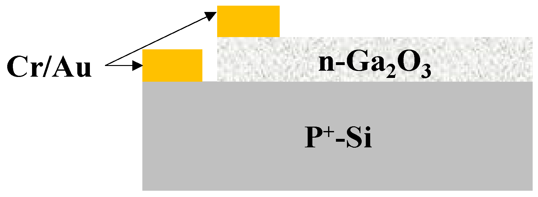
2. Materials and Methods

The UV photodetector was fabricated on (100) P+-Si substrate doped with phosphorus. The substrate was 500 μm thick and had a resistivity between 0.001 and 0.005 Ω-cm. Before each experiment, the silicon substrate was cleaned for 5 min in acetone and then, in methanol for 5 min in an ultrasonic bath. Following the cleaning procedure, the wafer was rinsed with deionized water for 5 min. To obtain Ga2O3, 0.2 g of gallium [(Ga) (purity 99.999%)] was dripped onto cleaned quartz crucible. Silver was used as a catalyst to enhance the growth of gallium oxide NWs. An ultrathin layer of 5 nm Ag was sputtered on silicon. The silicon wafer was positioned with the Ag-coated surface to face the crucible quartz containing Ga. The distance between the substrate and the gallium pool was 10 mm. Then, the substrate was loaded into a quartz crucible which was placed into an OTF-1200X-50-SL horizontal alumina tube furnace made by MTI Corporation (Richmond, CA, USA). The oxidation was performed at 950 °C for 1 h in a 20 sccm nitrogen atmosphere.
Figure 1 illustrates the setup of the UV photodetector fabrication process. As the system cools down to room temperature, the samples were removed from the furnace, cleaved, and characterized by scanning electron microcopy (SEM), X-ray photoelectron spectroscopy (XPS), and high-resolution transmission electron microscopy (HRTEM), equipped with energy dispersive X-ray spectroscopy. The electrical contacts were patterned on top of the nanowires using shadow mask and then 1 nm Cr and 150 nm Au were sputtered using a Lesker sputtering system. Electrical characterization of the system was also carried out to assess the performance of the UV photodetector. For electrical measurements, a custom probe station attached to a Keithly 2400 series SMU instrument was used. For photocurrent measurements, UV illumination was from a Dymax Bluewave 75 UV lamp (280–320 nm) (Dymax Corporation, Torrington, CT, USA). A light intensity of 1.5 W/cm2 was used.

3. Results and Discussion

3.1. Surface Morphology

Ga2O3 nanowires were grown on P+-Si at 950 °C. As shown in Figure 2, the silver catalyst plays a major role in the growth mechanism. Using 5 nm Ag as a catalyst, a homogeneous coating and denser nanowires were achieved due to the low contact angle. A low contact angle reflects the extension of wetting, i.e., the liquid advances on the surface and homogeneously wets the surface. To control the wetting contact angle, deposition or incorporation of elements and molecules onto the surface is a standard procedure. We believe that Ag has the role to improve wettability, which will enhance the homogeneous appearance of Ga2O3 nuclei that could lead to dense nanowires. The contact angle of Ga on a silver film is 30° [30], and on a silicon substrate, it is 73.9° [31], leading to better wetting of Ga on Ag surface and uniform growth of Ga2O3 nanowires (Figure 3).
Various research strategies were conducted in the past, mainly to enhance the nanowires’ growth on the target substrate [10,32,33,34]. In contrast, these techniques to grow Ga2O3 nanowires have shown lateral growth, overlapping nanowires, less dense and weak adhesion to the substrate. None of the previous techniques were able to produce a conformal growth process of Ga2O3 nanowires on the substrate surface.
The results obtained with the use of 5 nm Ag catalyst showed a remarkable improvement in the lengths and the density of the nanowires, most of them perpendicular to the surface. Even though the lengths of these nanowires were increased, their diameters were decreased. The diameters of the nanowires were in the range of 70–90 nm at the tip and 120–160 nm at the bottom. The average length of these nanowires was in the range of about 30–70 µm.

3.2. X-ray Photoelectron Spectroscopy (XPS)

To analyze the elemental composition of Ga2O3 nanowires, XPS was performed on a PHI 5800 model.
Figure 4 shows XPS spectra of Ga2O3 nanowires on Si. The XPS spectrum shows the chemical composition of the particles at the surface of β-Ga2O3 nanowires on Si in the presence of Ag. The binding energies of Ga2p3, O1s, and Ag3d (with two peaks) and Si2p are 1119.1 eV, 532 eV, 369.07 eV and 379.66 eV and 105.18 eV, respectively. The peaks of Ga and O for Ga2O3 and Ag are in agreement with the handbook of XPS spectra [35,36]. XPS analysis of the β-Ga2O3 nanowires on Si and the presence of Ag catalyst showed a positive shift due to the effect of the electronegativity difference [37]. In addition, this shift could be attained in Ag3d, as the size of Ag nanoparticles highly decreased [38].

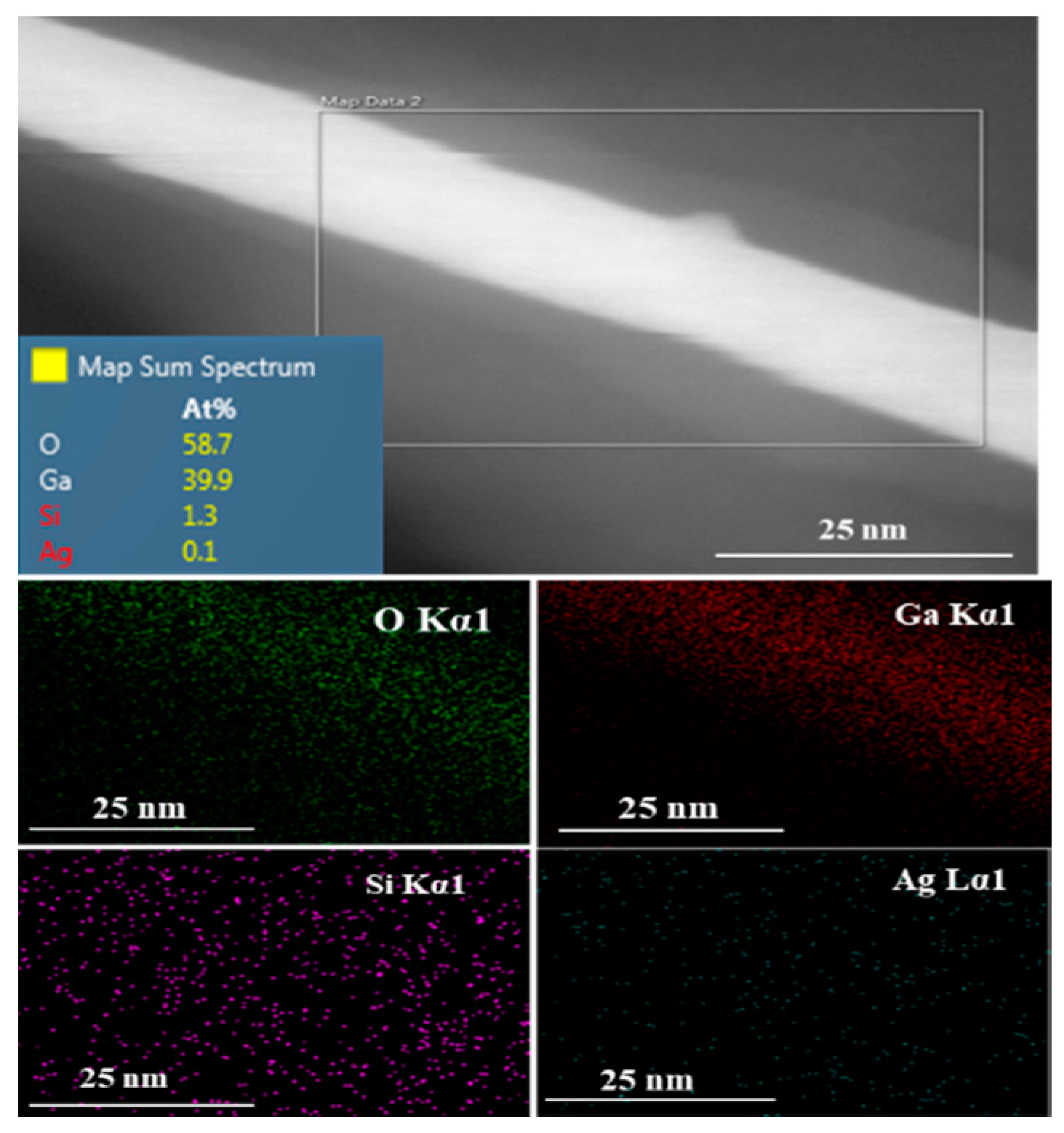
3.3. High-Resolution Transmission Electron Microscopy (HRTEM)/Energy-Dispersive Spectroscopy (EDS)

An energy-dispersive spectroscopy (EDS) profile analysis was performed on β-Ga2O3 nanowires grown on Si (Figure 5). Interestingly, none of the Ag nanoparticles were clearly observed on the surface of the nanowires. However, a very small amount in atomic percentage of Ag was detected by HRTEM equipped with EDS. Because no Ag was observed on the nanowire surface, a very small amount of Ag might be embedded into the Ga2O3 nanowires. These remaining Ag nanoparticles could be trapped inside the nanowires after all Ag was consumed and evaporated.
Because silicon atoms can interact with silver at a high temperature (i.e., the oxidation temperature of 950 °C) the background impurity of silicon was measured in Ga2O3 nanowires. At high temperature and a few atomic percentages of Si, the Si-Ag phase diagram [39] shows that Si can interact with Ag. Silicon is one of the major impurities that strongly correlates to n-type conductivity [40]. If silicon were to be incorporated into Ga2O3 nanowires during oxidation, it could increase the n-type conductivity of nanowires. In addition, since Si has a strong effect on the dissolution of the large Ag NPs [41], there will be more Ag atoms available for diffusion on the Si surface, which could result in a denser growth of nanowires.

3.4. Growth Mechanism of β-Ga2O3 Nanowires

The contribution of a silver catalyst to the growth enhancement of β-Ga2O3 nanowires on Si showed a growth reaction rate strongly influenced by the oxidation temperature and follows the Arrhenius law [42]. Oxygen diffusivity and solubility are important parameters that distinguish Ag as an effective catalyst for Ga2O3 nanowire growth.
Diffusion is a result of the kinetic properties of atoms. In this case, diffusion appears to be due to the high capability of Ag to absorb oxygen, and it is greatly influenced by the variation of temperature. Different studies were focused on the oxygen diffusivity ( D ) in gallium [43] and silver [44]. Table 1 summarizes the major diffusivity coefficient of oxygen into solid Ag, liquid silver, and liquid gallium. The diffusion coefficient of oxygen in silver has a high tendency to absorb oxygen, and hence, boost nanowire growth.
The solubility of oxygen is another factor that has essential perspective to speed up the growth of Ga2O3 nanowires. The activation energy of oxygen solubility in silver was 0.01192 eV/K at a temperature range of 763–937 °C [45]; however, in gallium, it was 2.38 × 10⁻⁴ eV/K at a temperature range of 750–1000 °C [48]. Oxygen solubility in silver exhibited a higher solubility than Ga. Further studies are needed to measure the Ag-Ga-O thermodynamics at higher temperatures.
Taking these results into consideration, the growth mechanism of nanowires can be explained as follows. First, at higher temperatures, the liquid gallium can form gallium oxide in the presence of oxygen. Then, the oxide is further reduced by liquid metallic gallium and forms a gas phase of gallium suboxide (Ga2O), as shown in Equation (1) [29,49] as follows:
Ga2O3(s) + 4Ga(l) → 3Ga2O(g)
The Ga2O gas phase is transported to the cooler regions and decomposes to liquid gallium and Ga2O3 [50,51], leading to a vapor-liquid-solid (VLS) growth mechanism. At high temperatures (T > 950 °C) denser Ga2O3 grows as nanowires. It has been shown that the presence of Ga atoms can easily etch the surface of silica substrate around 950 °C, as shown in Equation (2) [52].
SiO2+ 4Ga→ 2Ga2O ↑+ Si
In addition, the phase diagram of Si-Ag shows that a liquid phase exists in this system at high temperatures (T > 800 °C) at a small percentage of Si [39]. The contribution of small concentrations of silicon can detach and stimulate the melting point of Ag surface atoms [41]. Despite the fact that carrier doping in β-Ga2O3 is a difficult task, some impurity doping using Sn or Si has been shown to achieve electrical conduction [40,53,54,55]. In this growth mechanism, silicon has been detected by EDS (Figure 5), unintentionally improving the background conductivity of the nanowires. The presence of oxygen atoms segregated on the surface of Ag catalyst will react with Ga. This increases the flux of O atoms and Ga segregation at Ag-Si interface, leading to the formation of an equilibrium mixture of Ag-Si-Ga-O that becomes a solid phase source for Ga2O3 nucleation (Figure 6).

3.5. Electrical Characterization

3.5.1. I-V Characterization

The β-Ga2O3/P+-Si PN heterojunction (Figure 7) was fabricated to determine the electronic properties of β-Ga2O3 nanowires. The choice of testing the P+Si substrate is due to availability of low-cost materials for electronics and to observe how silicon from the substrate can influence the conductivity of Ga2O3. Impact of silicon doping in Ga2O3 during the growth processes were reported in references [40,53,54,55] for the cases of thin films and bulk materials and we wanted to investigate if migration of silicon atoms from the substrate can have a similar effect. In addition, the formation of n-Ga2O3 nanowires on the surface of highly doped silicon substrates has not been reported so far. The results lead to the development of a simple growth technique for large-scale production of a highly sensitive and stable structure. In previous works, the growth of Ga2O3 was obtained due to the presence of an Au catalyst (instead of Ag) on the surface of the Si2/Si template [28].
The current-voltage (I-V) characteristics were measured in dark conditions and under UV illumination at different voltages 10 and 50 V. Photocarriers, which were excited by UV illumination, were from a Dymax Bluewave 75 UV lamp (280–320 nm) (Dymax Corporation, Torrington, CT, USA) (Figure 8). The photoconductivity mechanism of the β-Ga2O3 NWs is credited to a surface oxygen adsorption and desorption process [56], which is highly influenced by the presence of silver as a catalyst, leading to improve oxygen detection and hence the electrical properties of the β-Ga2O3 nanowires.
The ratio of photo-to-dark current at 10 V was 3066.11 which is higher than other reported studies [57,58]. The reduction in performance could be attributed to the presence of Ag NPs, which were detected by XPS, although they are difficult to see in the scanning and transmission microscopy (SEM) images. The hot carriers of Ag NPs could increase the self-heating effects [59]. This issue is one of the major challenges that is still under investigation to improve the thermal conductivity of Ga2O3. It is well known that Ga2O3 generates self-heating effects that cause degradation of the carriers mobility [60], leading to reduced performance of Ga2O3 at high voltage.
Even the addition of Ag catalyst could cause a drawback, as it can enhance the sensitivity of the photodetector. The effect of the catalytic Ag nanoparticles can be explained as follows. First, Ag nanoparticles have a significant contribution in improving the conductivity of Ga2O3 nanowires, leading to better sensing performance. Secondly, Ag nanoparticles have the ability to greatly enhance the adsorption and desorption of O2 on their surface due to the highly conductive behavior of Ag metal [61]. Consequently, the number of electrons drawn to O2 increases greatly. Third, Ag nanoparticles play the role of electron mediators that allow electrons to migrate from the surface of Ga2O3 nanowires to the O2 through the defect states of Ga2O3. As a result, the bulk defects of Ga2O3 may act as a secondary factor in the sensing mechanism in addition to the surface defects [4]. Consequently, Ag NPs significantly reduce the density of electrons of Ga2O3 and improve electrical conductivity, leading to better selectivity and sensitivity.

3.5.2. Transient Time

The transient response of the photodetector was measured by turning on and off a UV light source with wavelength range from 280 to 450 nm (Figure 9). Under UV illumination, the oxygen adsorption and desorption processes are attained to improve the photoconductivity response by increasing the carrier mobility. In contrast, when UV illumination is switched off, the excess electrons and holes recombine rapidly. Ga2O3 on silicon with Ag catalyst showed a rapid transient response due to the enhanced carrier transport. The rise was 0.8 s and fall time was 1.5 s. Due to the enhanced carrier transport process, fast rise and decay of the photocurrent were obtained.

3.5.3. Detection Mechanism

In dark current measurements, Ag NPs cause a localized Schottky junction and deplete the carriers at the interface of β-Ga2O3 nanowires. Therefore, there is a large depletion width at the interface between Ag NPs and β-Ga2O3 nanowires, leading to a decrease in the dark current of the UV photodetector.
UV detection mechanism is determined based on the contribution of two different parts, namely, Ag nanoparticles catalyst and P+-silicon. Under UV illumination, when the photon energy is larger than the bandgap of Ga2O3, carriers (electron-hole pairs) are generated [hv → e + h+]. These enhanced photo-generated carriers by the large electric field increase the carrier density in β-Ga2O3 nanowires and improve the photocurrent response. The energy band diagrams of the AgNPs/ β-Ga2O3 /p-Si p-n junction is shown in Figure 10a. The band offsets values are estimated using the electron affinity 4.05 eV [62], 4.00 eV [63], and band gap 1.12 eV, 4.9 eV for p-Si, and β-Ga2O3, respectively. The work function (φGa2O3) and electron affinity (χGa2O3) of β-Ga2O3 are 4.11 eV and 4.00 eV [63], respectively. This is lower than the work function of Ag (4.26 eV), leading to the formation of a Schottky barrier which prevents the electrons transport from Ag NPs side to Ga2O3. In addition, Ag NPs on the surface of Ga2O3 is highly influenced with UV light below 320 nm due to the interband transitions, exciting the transition of highly energetic hot electrons from the 4d and 5-sp bands [64,65,66]. These hot electrons surmount the small height of Schottky barrier and lead to local band bending downward on the Ga2O3 side to enable the electron transfer to the conduction band of Ga2O3 nanowires.
Regarding the silicon contribution, when the applied voltage is positive on Ga2O3, the movement of holes can easily be achieved; hence, photocurrent response is increased. However, if the voltage is negative, the holes are constrained and cannot jump the hill to the side of p-Si. Consequently, the presence of more electrons can increase oxygen molecules absorption and ionization [O2+ e → O2 [ad]] [67,68]. However, the holes drift to the surface, accumulate, recombine with adsorbed ionized oxygen and form free oxygen molecules from the surface [O2 [ad] + h+ → O2]. The remaining electrons become the majority carriers that contribute to an increase in the photocurrent by generation and recombination until reaching an equilibrium phase.
Nanowires offer a great opportunity to form a higher density of exposed surface states due to the dangling bonds at the surface of nanowires. These trap states of oxygen generated at the surface of Ga2O3 nanowires have a large impact on device performance [2]. The detector can be easily and fully integrated on a chip with proper metal contacts similar to the graphene-based detectors [69]. Due to the large surface to volume ratio of nanowires and the existence of Ag NPs, the surface of NWs with trapped oxygen becomes highly sensitive.

4. Conclusions

Highly oriented, dense, and long β-Ga2O3 nanowires were grown on P+-Si (100) substrate in the presence of a 5 nm thin film of Ag catalyst and oxidation treatment at high temperature (1000 °C). Silver was shown to have a great impact to expedite the growth of Ga2O3 nanowires and retain their physical and chemical properties. The morphological, compositional, and electrical properties were explored. The growth mechanism of nanowires on the silicon substrate was discussed. During the growth process, Ga2O3 nanowires are highly influenced by silicon as unintentional impurities that increase the n-type doping. The photoresponse under UV irradiation was excellent. The ratio of photo-to-dark current (Iphoto/Idark) was measured to be around 3.07 × 10³ at 10 V. The high photosensitivity could be attributed to the higher electron density in Ga2O3 nanowires with Ag NPs. The carrier transport process was shown to have a fast response. The energy band gap and carrier dynamics at the interfaces were discussed. This synthesis can be optimized for sensing, electronics, and photonic applications.

Author Contributions

Conceptualization, B.A.; Methodology, B.A.; Resources, M.S.I.; Data Curation, B.A.; Writing—Original Draft Preparation, B.A.; Writing—Review & Editing, B.A., R.V. and M.S.I.; Supervision, M.S.I.; Project Administration, M.S.I.; Funding Acquisition, M.S.I.

Funding

This research received no external funding

Acknowledgments

The author gratefully acknowledged the financial support by Kuwait Institute for Scientific Research.

Conflicts of Interest

The authors declare no conflict of interest.

References

  1. González-Posada, R.S.F.; den Hertog, M.; Monroy, E. Room-Temperature Photodetection Dynamics of Single GaN Nanowires. Nano Lett. 2012, 12, 172–176. [Google Scholar] [CrossRef]
  2. Weng, W.Y.; Hsueh, T.J.; Chang, S.J.; Huang, G.J.; Hsueh, H.T. A beta-Ga2O3 Solar-Blind Photodetector Prepared by Furnace Oxidization of GaN Thin Film. IEEE Sens. J. 2011, 11, 999–1003. [Google Scholar] [CrossRef]
  3. Mazeina, L.; Perkins, F.K.; Bermudez, V.M.; Arnold, S.P.; Prokes, S.M. Functionalized Ga2O3 Nanowires as Active Material in Room Temperature Capacitance-Based Gas Sensors. Langmuir 2010, 26, 13722–13726. [Google Scholar] [CrossRef]
  4. Lin, H.J.; Baltrus, J.P.; Gao, H.; Ding, Y.; Nam, C.Y.; Ohodnicki, P.; Gao, P.X. Perovskite Nanoparticle-Sensitized Ga2O3 Nanorod Arrays for CO Detection at High Temperature. ACS Appl. Mater. Interface. 2016, 8, 8880–8887. [Google Scholar] [CrossRef]
  5. Mao, A.K.H.; Gao, J.; Chopdekar, R.; Takamura, Y.; Chowdhury, S.; Islam, M.S. An Investigation of Electrical and Dielectric Parameters of Sol-Gel Process Enabled beta-Ga2O3 as a Gate Dielectric Material. IEEE Trans. Elect. Devices 2017, 64, 2047–2053. [Google Scholar]
  6. Pearton, S.J.; Yang, J.; Carey, P.; Ren, F.; Kim, J.; Tadjer, M.J.; Mastro, M.A. A review of Ga2O3 materials, processing, and devices. Appl. Phys. Rev. 2018, 5, 011301. [Google Scholar] [CrossRef]
  7. Kaya, A. β-Ga2O3 films grown via oxidation of GaAs substrates and their device demonstrations. In Proceedings of the Wide Bandgap Power Devices and Applications II SPIE, San Diego, CA, USA, 7–8 August 2017. [Google Scholar]
  8. Patil-Chaudhari, D.; Ombaba, M.; Oh, J.Y.; Mao, H.; Montgomery, K.; Lange, A.; Mahajan, S.; Woodall, J.M.; Islam, M.S. Solar Blind Photodetectors Enabled by Nanotextured β-Ga2O3 Films Grown via Oxidation of GaAs Substrates. IEEE Photon. J. 2017, 9, 1–7. [Google Scholar] [CrossRef]
  9. Otsuka, S.; Katayama, I.; Kozuka, Z. Measurements of Diffusivity of Oxygen in Liquid Silver by Potentiostatic Methods Employing Solid Electrolyte. Trans. Jpn. Inst. Met. 1971, 12, 442–447. [Google Scholar] [CrossRef]
  10. Nguyen, T.D.; Kim, E.T.; Dao, K.A. Ag nanoparticle catalyst based on Ga2O3/GaAs semiconductor nanowire growth by VLS method. J. Mater. Sci. Mater. Electron. 2015, 26, 8747–8752. [Google Scholar] [CrossRef]
  11. Guo, D.; Wu, Z.; Li, P.; Wang, Q.; Lei, M.; Lie, L.; Tang, W. Magnetic anisotropy and deep ultraviolet photoresponse characteristics in Ga2O3: Cr vermicular nanowire thin film nanostructure. RSC Adv. 2015, 5, 12894–12898. [Google Scholar] [CrossRef]
  12. Lee, S.Y.; Choi, K.H.; Kang, H.C. Growth mechanism of In-doped beta- Ga2O3 nanowires deposited by radio frequency powder sputtering. Mater. Lett. 2016, 176, 213–218. [Google Scholar] [CrossRef]
  13. Choi, K.H.; Cho, K.K.; Kim, K.W.; Cho, G.B.; Ahn, H.J.; Nam, T.H. Catalytic Growth and Structural Characterization of Semiconducting beta-Ga2O3 Nanowires. J. Nanosci. Nanotechnol. 2009, 9, 3728–3733. [Google Scholar] [CrossRef] [PubMed]
  14. Park, S.; Sun, G.J.; Lee, C. UV-assisted room temperature-gas sensing of Ga2O3-core/ZnO-shell nanowires. J. Ceram. Process. Res. 2015, 16, 367–371. [Google Scholar]
  15. Jang, Y.G.; Kim, W.S.; Kim, D.H.; Hong, S.H. Fabrication of Ga2O3/SnO2 core-shell nanowires and their ethanol gas sensing properties. J. Mater. Res. 2011, 26, 2322–2327. [Google Scholar] [CrossRef]
  16. Ghose, S.; Rahman, M.S.; Arias, A.; Rojas-Ramirez, J.S.; Caro, M.; Nedev, N.; Droopad, R. Structural and optical properties of beta-Ga2O3 thin films grown by plasma-assisted molecular beam epitaxy. J. Vac. Sci. Technol. B 2016, 34. [Google Scholar] [CrossRef]
  17. Feng, Q.; Li, F.; Dai, B.; Jia, Z.; Xie, W.; Xu, T.; Lu, X.; Tao, X.; Zhang, J.; Hao, Y. The properties of gallium oxide thin film grown by pulsed laser deposition. Appl. Surf. Sci. 2015, 359, 847–852. [Google Scholar] [CrossRef]
  18. Han, W.Q.; Kohler-Redlich, P.; Ernst, F.; Ruhle, M. Growth and microstructure of Ga2O3 nanorods. Solid State Commun. 2000, 115, 527–529. [Google Scholar] [CrossRef]
  19. Cao, C.B.; Chen, Z.; An, X.Q.; Zhu, H.S. Growth and field emission properties of cactus-like gallium oxide nanostructures. J. Phys. Chem. C 2008, 112, 95–98. [Google Scholar] [CrossRef]
  20. Sharma, S.; Sunkara, M.K. Direct synthesis of gallium oxide tubes, nanowires, and nanopaintbrushes. J. Am. Chem. Soc. 2002, 124, 12288–12293. [Google Scholar] [CrossRef]
  21. Pallister, P.J.; Buttera, S.C.; Barry, S.T. Self-seeding gallium oxide nanowire growth by pulsed chemical vapor deposition. Phys. Status Solidi Appl. Mater. Sci. 2015, 212, 1514–1518. [Google Scholar] [CrossRef]
  22. Zhao, Y.Y.; Frost, R.L.; Yang, J.; Martens, W.N. Size and morphology control of gallium oxide hydroxide GaO(OH), nano- to micro-sized particles by soft-chemistry route without surfactant. J. Phys. Chem. C 2008, 112, 3568–3579. [Google Scholar] [CrossRef]
  23. Reddy, L.S.; Ko, Y.H.; Yu, J.S. Hydrothermal Synthesis and Photocatalytic Property of beta-Ga2O3 Nanorods. Nanoscale Res. Lett. 2015, 10, 364. [Google Scholar] [CrossRef] [PubMed]
  24. Dai, X.; Zhang, S.; Wang, Z.; Adamo, G.; Liu, H.; Huang, Y.; Couteau, C.; Soci, C. GaAs/AlGaAs Nanowire Photodetector. Nano Lett. 2014, 14, 2688–2693. [Google Scholar] [CrossRef]
  25. Alhalaili, B.; Mao, H.; Islam, M.S. Ga2O3 Nanowire Synthesis and Device Applications. In Novel Nanomaterials—Synthesis and Applications; IntechOpen Limited: London, UK, 2017; Volume 2. [Google Scholar]
  26. Ogita, M.; Higo, K.; Nakanishi, Y.; Hatanaka, Y. Ga2O3 thin film for oxygen sensor at high temperature. Appl. Surf. Sci. 2001, 175–176, 721–725. [Google Scholar] [CrossRef]
  27. Kim, H.W.; Kim, N.H.; Lee, C. Growth of Ga2O3 thin films on Si (100) substrates using a trimethylgallium and oxygen mixture. J. Mater. Sci. 2004, 39, 3461–3463. [Google Scholar] [CrossRef]
  28. Wu, Y.L.; Chang, S.-J.; Weng, W.-Y.; Liu, C.; Tsai, T.Y.; Hsu, C.-L.; Chen, K.C. Ga2O3 Nanowire Photodetector Prepared on SiO2/Si Template. IEEE Sens. J. 2013, 13, 2368–2373. [Google Scholar] [CrossRef]
  29. Alhalaili, B.; Bunk, R.; Vidu, R.; Islam, M.S. Dynamics Contributions to the Growth Mechanism of Ga2O3 Thin Film and NWs Enabled by Ag Catalyst. Nanomaterials 2019, 9, 1272. [Google Scholar] [CrossRef]
  30. Glickman, E.; Levenshtein, M.; Budic, L.; Eliaz, N. Interaction of liquid and solid gallium with thin silver films: Synchronized spreading and penetration. Acta Mater. 2011, 59, 914–926. [Google Scholar] [CrossRef]
  31. Detz, H.; Kriz, M.; MacFarland, D.; Lancaster, S.; Zederbauer, T.; Capriotti, M.; Andrews, A.M.; Schrenk, W.; Strasser, G. Nucleation of Ga droplets on Si and SiOx surfaces. Nanotechnology 2015, 26. [Google Scholar] [CrossRef]
  32. Mao, H.; Alhalaili, B.; Kaya, A.; Dryden, D.M.; Woodall, J.M.; Islam, M.S. Oxidation of GaAs substrates to enable β-Ga2O3 films for sensors and optoelectronic devices (SPIE Optical Engineering + Applications). In Proceedings of the Wide Bandgap Power Devices and Applications II, San Diego, CA, USA, 7–8 August 2017. [Google Scholar]
  33. Song, P.Y.; Wu, Z.Y.; Shen, X.Y.; Kang, J.Y.; Fang, Z.L.; Zhang, T.Y. Self-consistent growth of single-crystalline ((2)over-bar01) beta-Ga2O3 nanowires using a flexible GaN seed nanocrystal. Crystengcomm 2017, 19, 625–631. [Google Scholar] [CrossRef]
  34. Chun, H.J.; Choi, Y.S.; Bae, S.Y.; Seo, H.W.; Hong, S.J.; Park, J.; Yang, H. Controlled structure of gallium oxide nanowires. J. Phys. Chem. B 2003, 107, 9042–9046. [Google Scholar] [CrossRef]
  35. Crist, V. Handbook of Monochromatic XPS Spectra: The Elements of Native Oxides; Wiley-VCH: Wenheim, Germany, 2000. [Google Scholar]
  36. Logofatu, C.; Negrila, C.C.; Ghita, R.V.; Ungureanu, F.; Cotirlan, C.; Manea, C.G.A.S.; Lazarescu, M.F. Study of SiO2/Si Interface by Surface Techniques. Cryst. Silicon Prop. Uses 2011, 23–42. [Google Scholar] [CrossRef]
  37. Dong, C.Y.; Shang, D.S.; Shi, L.; Sun, J.; Shen, B.G.; Zhuge, F.; Li, R.-W.; Chen, W. Roles of silver oxide in the bipolar resistance switching devices with silver electrode. Appl. Phys. Lett. 2011, 98. [Google Scholar] [CrossRef]
  38. Salido, I.L. Electronic and Geometric Properties of Silver and Gold Nanoparticles. Ph.D. Thesis, University of Konstanz, Konstanz, Germany, 2007. [Google Scholar]
  39. Chevalier, P.Y. Thermodynamic Evaluation of the Ag-Si System. Thermochim. Acta 1988, 130, 33–41. [Google Scholar] [CrossRef]
  40. Varley, J.B.; Weber, J.R.; Janotti, A.; van de Walle, C.G. Oxygen vacancies and donor impurities in beta-Ga2O3. Appl. Phys. Lett. 2010, 97. [Google Scholar] [CrossRef]
  41. Gould, A.L.; Kadkhodazadeh, S.; Wagner, J.B.; Catlow, C.R.A.; Logsdail, A.J.; di Vece, M. Understanding the Thermal Stability of Silver Nanoparticles Embedded in a-Si. J. Phys. Chem. C 2015, 119, 23767–23773. [Google Scholar] [CrossRef] [Green Version]
  42. Zinkevich, M.; Aldinger, F. Thermodynamic assessment of the gallium-oxygen system. J. Am. Ceram. Soc. 2004, 87, 683–691. [Google Scholar] [CrossRef]
  43. Klinedinst, K.A.; Stevenson, D.A. Oxygen Diffusion in Liquid Gallium and Indium. J. Electrochem. Soc. 1973, 120, 304–308. [Google Scholar] [CrossRef]
  44. Zhou, Z.Y.; Ma, Y.M.; Han, Q.F.; Liu, Y.L. Solubility, permeation, and capturing of impurity oxygen in Au/Ag: A comparative investigation from first-principles. Comput. Mater. Sci. 2016, 114, 79–85. [Google Scholar] [CrossRef]
  45. Ramanarayanan, T.A.; Rapp, R.A. The Diffusivity and Solubility of Oxygen in Liquid Tin and Solid Silver and the Diffusivity of Oxygen in Solid Nickel. Metall. Trans. 1972, 3, 3239–3246. [Google Scholar] [CrossRef]
  46. Park, J.H. Measuring Oxygen Diffusivity and Solubility in Solid Silver with a Gas-Tight Electrochemical-Cell. Mater. Lett. 1990, 9, 313–316. [Google Scholar] [CrossRef]
  47. Kontoulis, I.; Steele, B.C.H. Determination of Oxygen Diffusion in Solid Ag by an Electrochemical Technique. Solid State Ion. 1991, 47, 317–324. [Google Scholar] [CrossRef]
  48. Heshmatpour, B.; Stevenson, D.A. An Electrochemical Study of the Solubility and Diffusivity of Oxygen in the Respective Liquid-Metals Indium, Gallium, Antimony and Bismuth. J. Electroanal. Chem. 1981, 130, 47–55. [Google Scholar] [CrossRef]
  49. Girija, K.; Thirumalairajan, S.; Mastelaro, V.R.; Mangalaraj, D. Catalyst free vapor–solid deposition of morphologically different β-Ga2O3 nanostructure thin films for selective CO gas sensors at low temperature. Anal. Method 2016, 3224–3235. [Google Scholar] [CrossRef]
  50. Butt, D.P.; Park, Y.; Taylor, T.N. Thermal vaporization and deposition of gallium oxide in hydrogen. J. Nucl. Mater. 1999, 264, 71–77. [Google Scholar] [CrossRef]
  51. Kumar, S.; Singh, R. Nanofunctional gallium oxide (Ga2O3) nanowires/nanostructures and their applications in nanodevices. Phys. Status Solidi Rapid Res. Lett. 2013, 7, 781–792. [Google Scholar] [CrossRef]
  52. Xu, C.; Chung, S.; Kim, M.; Kim, D.E.; Chon, B.; Hong, S.; Joo, T. Doping of Si into GaN nanowires and optical properties of resulting composites. J. Nanosci. Nanotechnol. 2005, 5, 530–535. [Google Scholar] [CrossRef]
  53. Walukiewicz, W. Intrinsic limitations to the doping of wide-gap semiconductors. Phys. B 2001, 302, 123–134. [Google Scholar] [CrossRef]
  54. Matsuzaki, K.; Yanagi, H.; Kamiyab, T. Field-induced current modulation in epitaxial film of deep-ultraviolet transparent oxide semiconductor Ga2O3. Appl. Phys. Lett. 2006, 88. [Google Scholar] [CrossRef]
  55. Villora, E.G.; Shimamura, K.; Yoshikawa, Y.; Ujiie, T.; Aoki, K. Electrical conductivity and carrier concentration control in beta-Ga2O3 by Si doping. Appl. Phys. Lett. 2008, 92. [Google Scholar] [CrossRef]
  56. Shao, D.L.; Yu, M.P.; Sun, H.T.; Hu, T.; Lian, J.; Sawyer, S. High responsivity, fast ultraviolet photodetector fabricated from ZnO nanoparticle-graphene core-shell structures. Nanoscale 2013, 5, 3664–3667. [Google Scholar] [CrossRef]
  57. Oh, S.; Mastro, M.A.; Tadjer, M.J.; Kim, J. Solar-Blind Metal-Semiconductor-Metal Photodetectors Based on an Exfoliated beta- Ga2O3 Micro-Flake. ECS J. Solid State Sci. Technol. 2017, 6, Q79–Q83. [Google Scholar] [CrossRef]
  58. Guo, D.Y.; Wu, Z.; An, Y.H.; Guo, X.; Chu, X.L.; Sun, C.L.; Li, L.; Li, P.G.; Tang, W.H. Oxygen vacancy tuned Ohmic-Schottky conversion for enhanced performance in β-Ga2O3 solar-blind ultraviolet photodetectors. Appl. Phys. Lett. 2014, 105, 023507. [Google Scholar] [CrossRef]
  59. Manjavacas, A.; Liu, J.; Kulkarni, V.; Nordlander, P. Plasmon-Induced Hot Carriers in Metallic Nanoparticles. ACS Nano 2014, 8, 7630–7638. [Google Scholar] [CrossRef]
  60. Oh, J.; Ma, J.; Yoo, G. Simulation study of reduced self-heating in β-Ga2O3 MOSFET on a nano-crystalline diamond substrate. Results Phys. 2019, 13, 102151. [Google Scholar] [CrossRef]
  61. Kleyn, A.W.; Butler, D.A.; Raukema, A. Dynamics of the interaction of O2 with silver surfaces. Surf. Sci. 1996, 363, 29–41. [Google Scholar] [CrossRef]
  62. Hou, Y.N.; Mei, Z.X.; Liang, H.L.; Ye, D.Q.; Liang, S.; Gu, C.Z.; Du, X.L. Comparative study of n-MgZnO/p-Si ultraviolet-B photodetector performance with different device structures. Appl. Phys. Lett. 2011, 98, 263501. [Google Scholar] [CrossRef] [Green Version]
  63. Mohamed, M.; Irmscher, K.; Janowitz, C.; Galazka, Z.; Manzke, R.; Fornari, R. Schottky barrier height of Au on the transparent semiconducting oxide beta-Ga2O3. Appl. Phys. Lett. 2012, 101. [Google Scholar] [CrossRef]
  64. Aslam, U.; Rao, V.G.; Chavez, S.; Linic, S. Catalytic conversion of solar to chemical energy on plasmonic metal nanostructures. Nat. Catal. 2018, 1, 656–665. [Google Scholar] [CrossRef]
  65. Emilio, M.G.; Alarcon, I.; Klas, I.U. Silver Nanoparticle Applications: In the Fabrication and Design of Medical and Biosensing Devices; Springer Berlin Heidelberg: New York, NY, USA, 2015. [Google Scholar]
  66. Arora, K.; Kumar, V.; Kumar, M. Silver plasmonic density tuned polarity switching and anomalous behaviour of high performance self-powered β-gallium oxide solar blind photodetector. arXiv 2018, arXiv:1809.10724. Available online: https://arxiv.org/pdf/1809.10724 (accessed on 25 October 2019).
  67. Soci, C.; Zhang, A.; Xiang, B.; Dayeh, S.A.; Aplin, D.P.; Park, J.; Bao, X.Y.; Lo, Y.H.; Wang, D. ZnO nanowire UV photodetectors with high internal gain. Nano Lett. 2007, 7, 1003–1009. [Google Scholar] [CrossRef] [PubMed]
  68. Prades, J.D.; Hernandez-Ramirez, F.; Jimenez-Diaz, R.; Manzanares, M.; Andreu, T.; Cirera, A.; Romano-Rodriguez, A.; Morante, J.R. The effects of electron-hole separation on the photoconductivity of individual metal oxide nanowires. Nanotechnology 2008, 19. [Google Scholar] [CrossRef] [PubMed] [Green Version]
  69. Ding, Y.; Guan, X.; Zhu, X.; Hu, H.; Bozhevolnyi, S.I.; Oxenloewe, L.K.; Jin, K.; Mortensen, N.A.; Xiao, S. Effective electro-optic modulation in low-loss graphene-plasmonic slot waveguides. Nanoscale 2017, 9. [Google Scholar] [CrossRef] [PubMed] [Green Version]
Figure 1. Schematic of the growth process of Ga2O3 NWs on Si substrate coated with 5 nm thin film of Ag and positioned downward to face liquid Ga pool in a quartz crucible. The distance between Ga pool and silicon substrate is about a ~10 mm gap.
Sensors 19 05301 g001
Figure 2. SEM images of Ga2O3 nanowires growth on Si at 950 °C (a) Top view and (b) Side view of Ga2O3 nanowires growth on Si. Denser and longer growth of nanowires were attained.
Sensors 19 05301 g002
Figure 3. Contact angle of liquid Ga droplet on different surfaces. (a) Silicon. (b) 5 nm silver thin film. Areas coated with 5 nm Ag show uniform and high-dense growth of Ga2O3 nanowires.
Sensors 19 05301 g003
Figure 4. XPS of the β-Ga2O3 nanowires was obtained at 950 °C and in the presence of an Ag catalyst. Different peaks were detected by XPS. (a) Ga. (b) O. (c) Ag. (d) Si. The peaks of Ag and Ga have positive slight shifts due to the difference in electronegativity and work function.
Sensors 19 05301 g004
Figure 5. HRTEM image and the corresponding EDS mapping of Ga, O, Si and Ag of Ga2O3 NWs on P-doped (100) silicon substrate coated with 5 nm Ag.
Sensors 19 05301 g005
Figure 6. The growth mechanism of Ga2O3 NW on a silicon substrate coated with 5 nm Ag as a catalyst. The equilibrium liquid mixture of Ag-Ga-O at higher temperature (>900 °C) leads to the enhancement of the growth mechanism and increases the density of Ga2O3 NWs.
Sensors 19 05301 g006
Figure 7. Schematic diagram of Au/β-Ga2O3/Silicon photoconductor. The distance between the gold probes is 0.8 mm.
Sensors 19 05301 g007
Figure 8. Semi-logarithmic plots of current density of dark and photocurrent characteristics of Ga2O3 NWs grown on silicon substrate at 950 °C with an Ag catalyst at 10 V, (a) 10 V, (b) 50 V.
Sensors 19 05301 g008
Figure 9. Transient response of the UV photodetector fabricated with Ag catalyst based on Au/β-Ga2O3/Silicon photojunction at 10 V.
Sensors 19 05301 g009
Figure 10. Energy band diagram of Ag NPs and Ga2O3 NWs pn P+-Si. (a) at the interface before contact. (b) Under UV illumination, the interband transition in Ag NPs enhances the photosensitivity of the UV detection, and more photo-generated holes of Ga2O3 NWs migrate to the surface by band bending.
Sensors 19 05301 g010
Table 1. Summary of reported diffusivity coefficient and activation energy of oxygen in silver and gallium.
MetalDiffusion Coefficient (D)(cm2/s)Activation Energy (EA) (eV/K)T (°C)YearRef.
Ags1.79 × 10−30.58127–9772016[44]
4.90 × 10−30.56740–9151972[45]
3.66 × 10−30.481990[46]
4.98 × 10−30.631991[47]
Agl20.1 × 10−40.91980–11301971[9]
4.9 × 10−30.12763–9371972[45]
Gal4.1 × 10−38.9 × 10−5750–9501981[43]
2.27 × 10−38.33 × 10−5750–10001972[48]

