Design of a 900 MHz Dual-Mode SWIPT for Low-Power IoT Devices

 ,
,  , , and
Abstract
:1. Introduction
2. System Architecture and Building Blocks
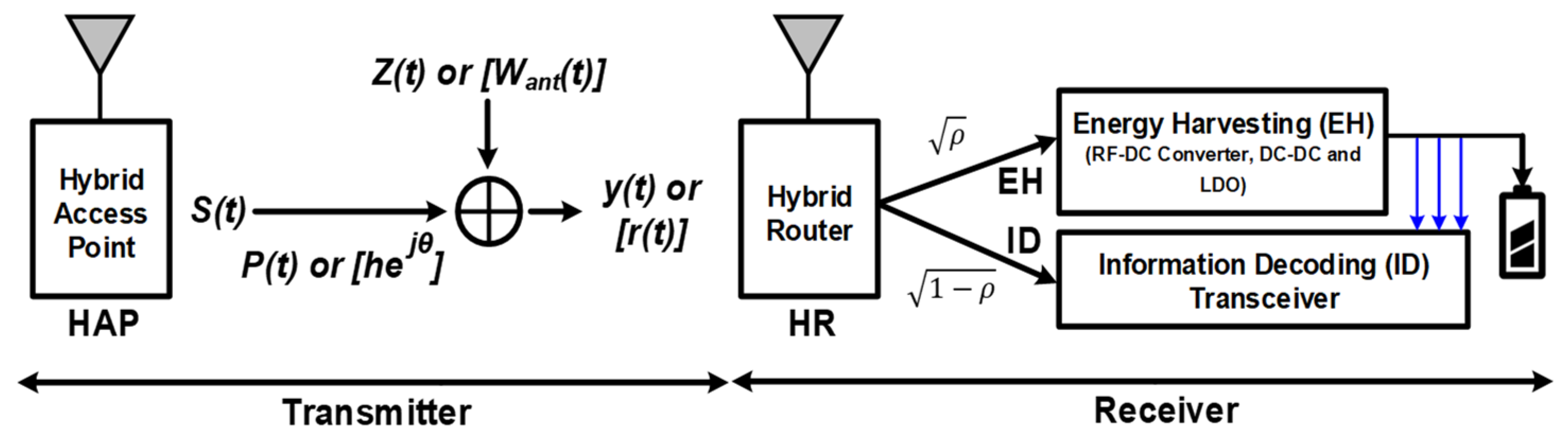
2.1. System Model
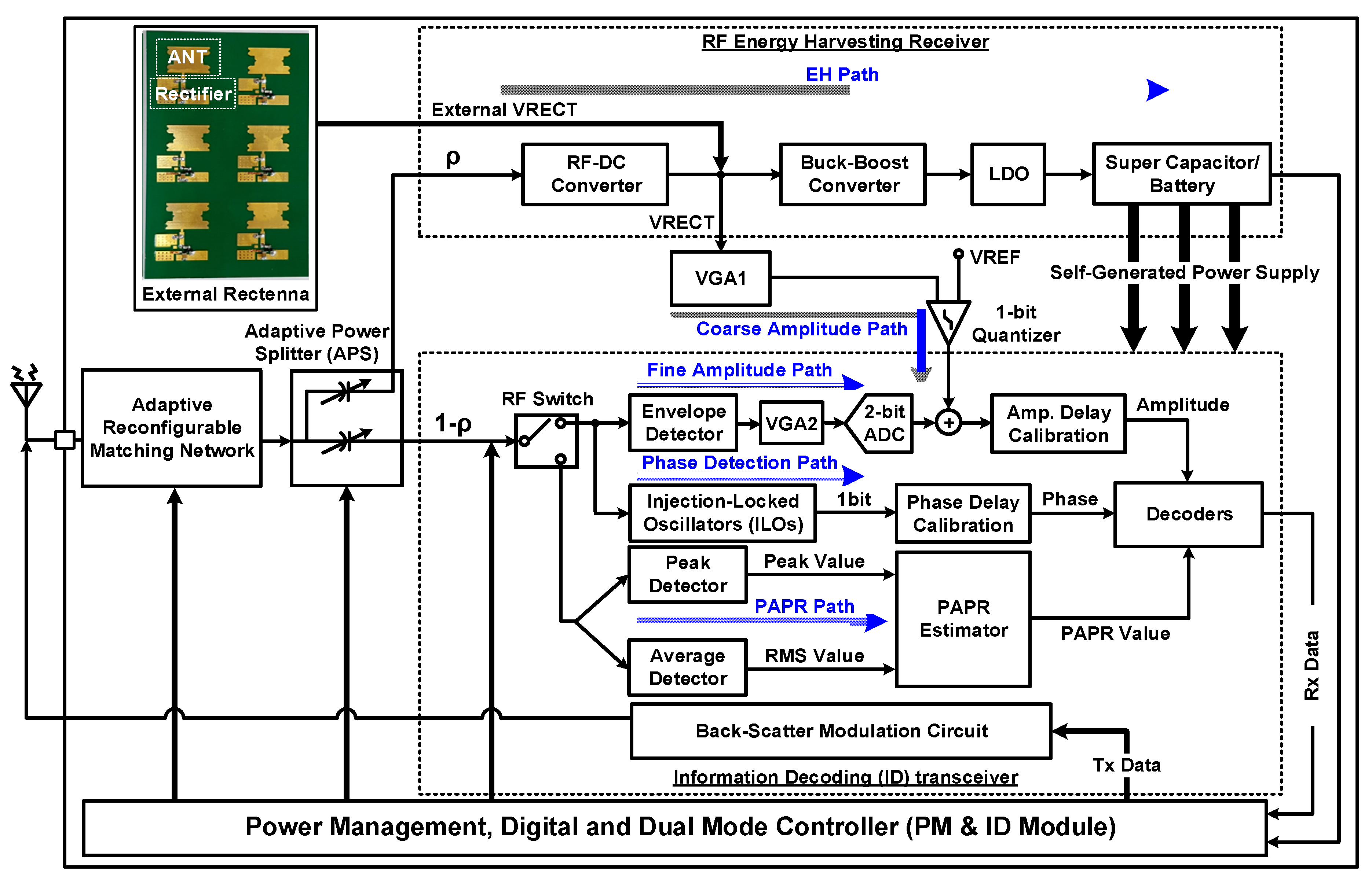
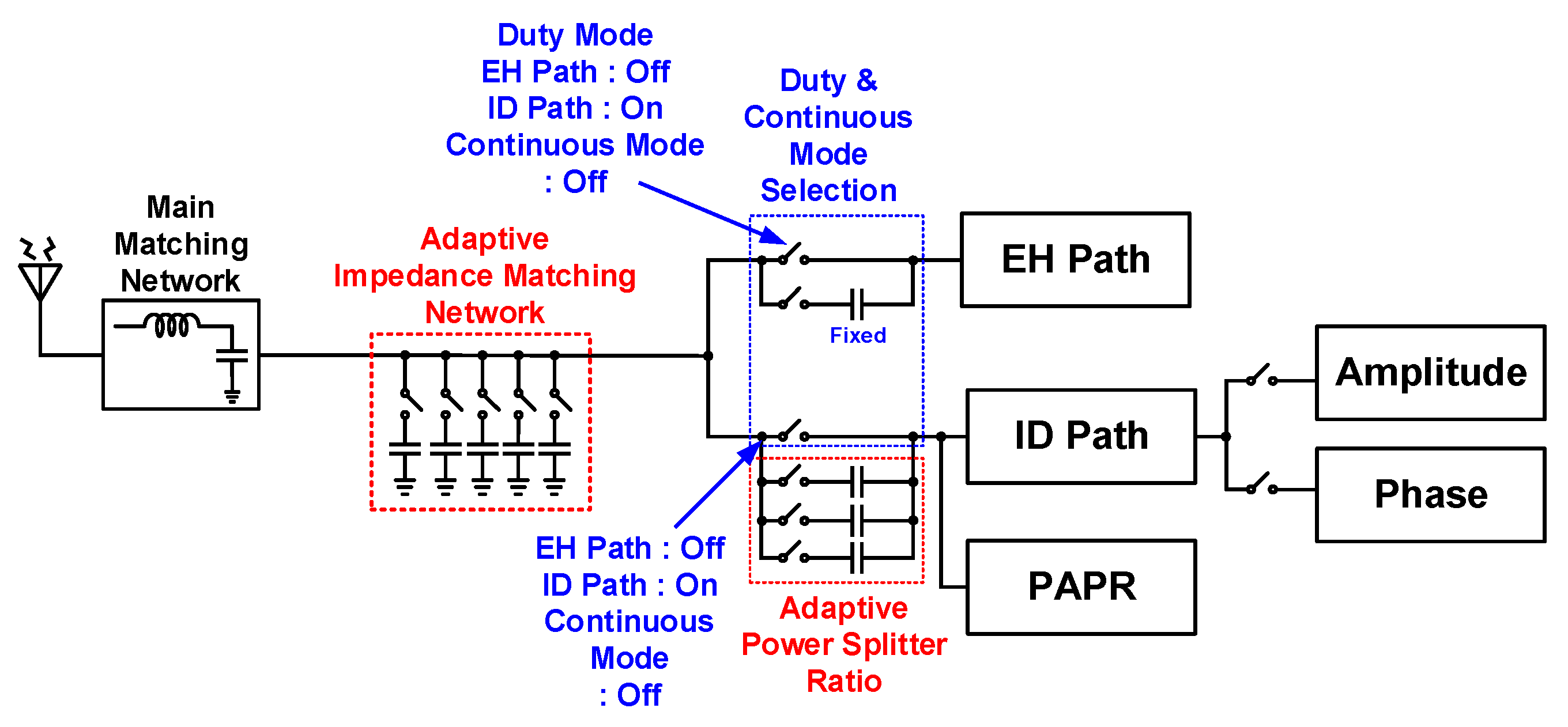
2.2. Architecture
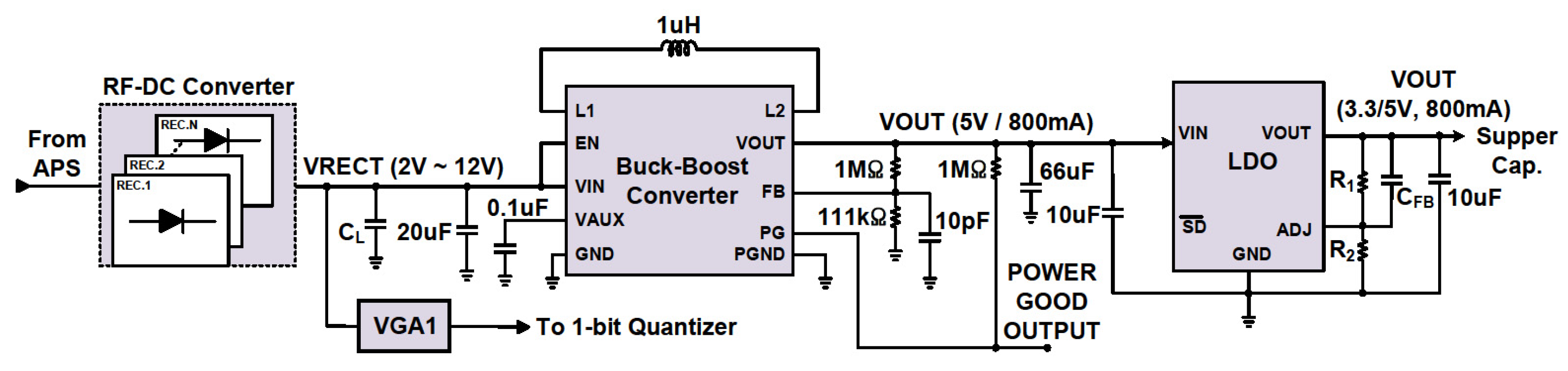
2.3. Energy Harvesting Path
- Case I: High-input power level ()
- Case II: Low-input power level ()
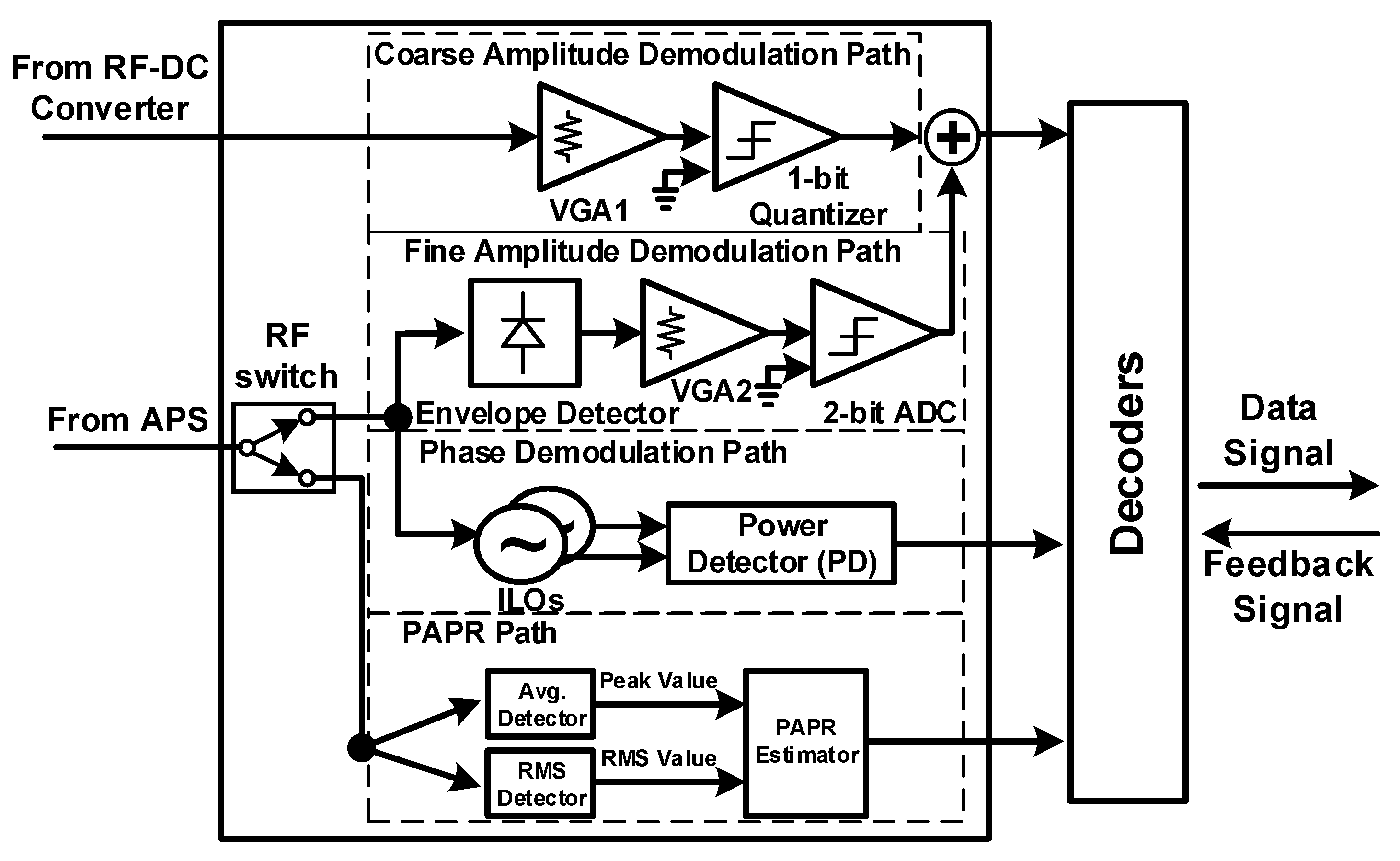
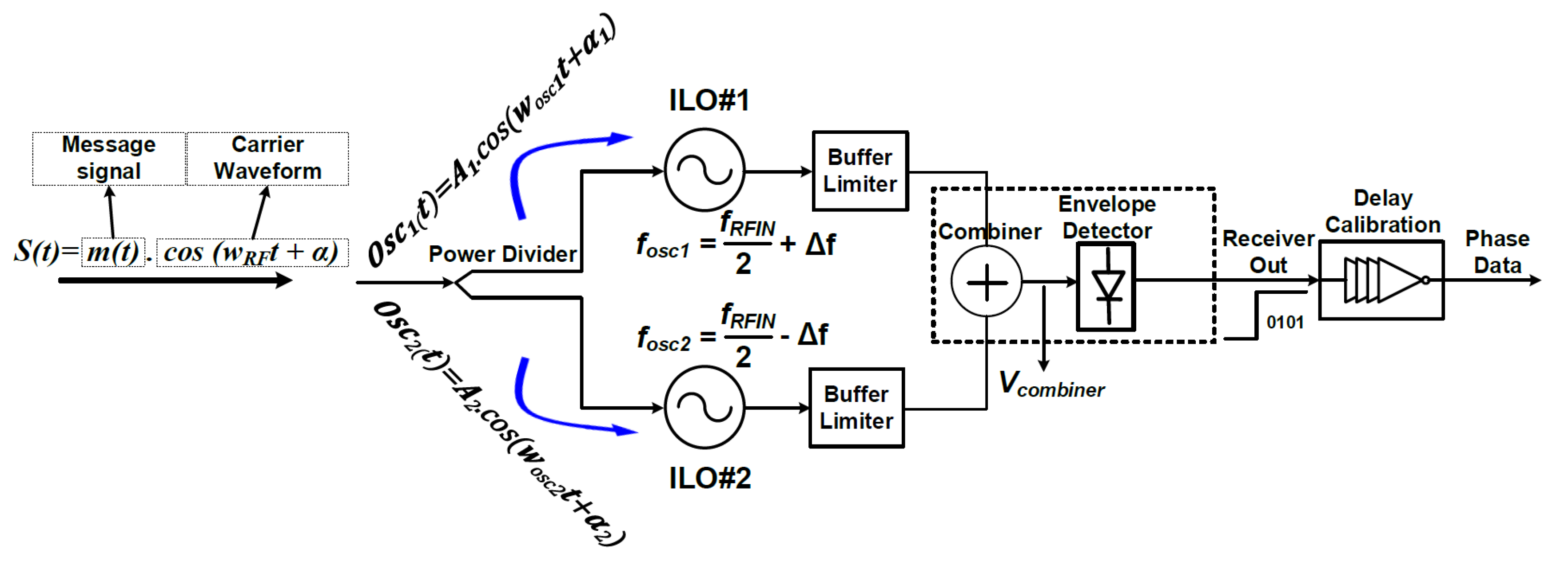
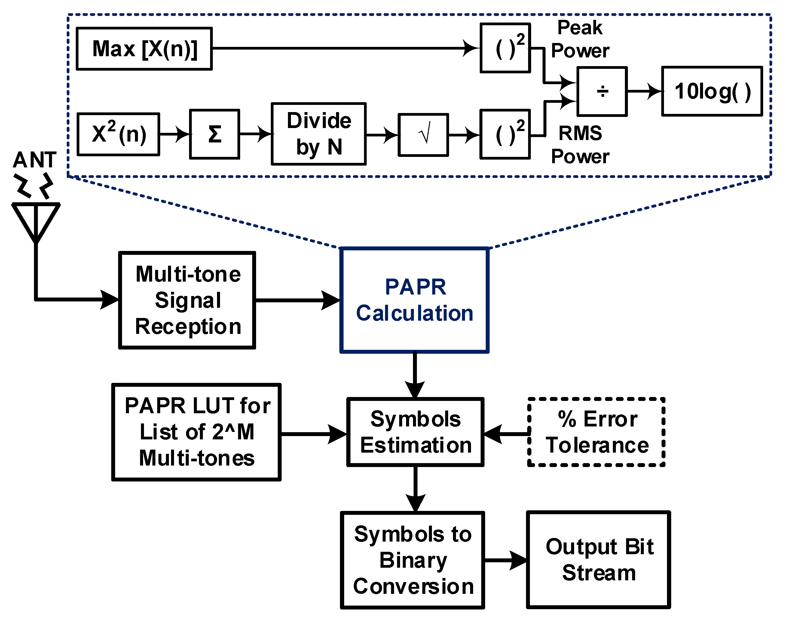
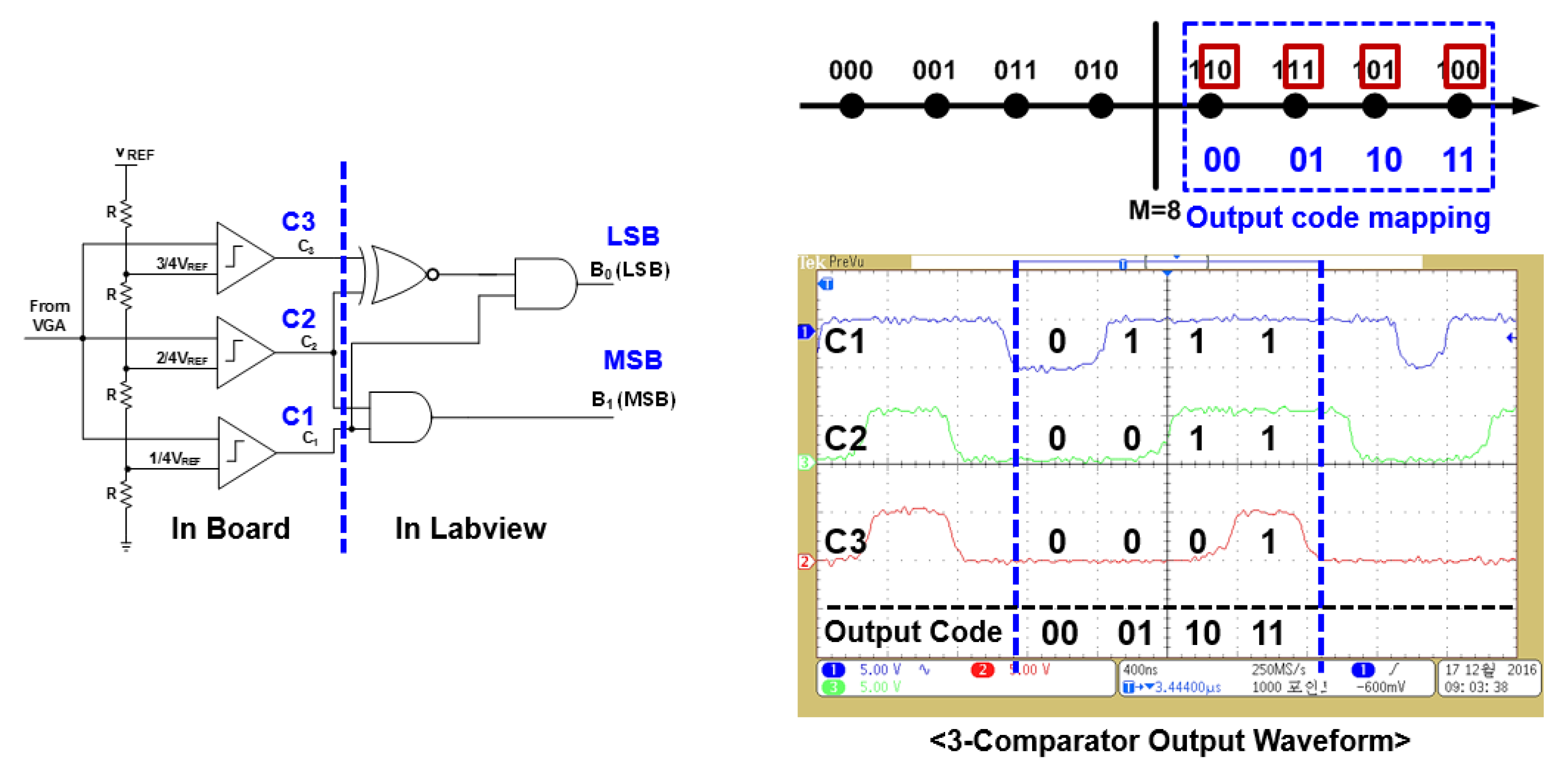
2.4. Information Decoding Path and PAPR Path
2.5. Backscatter Modulator
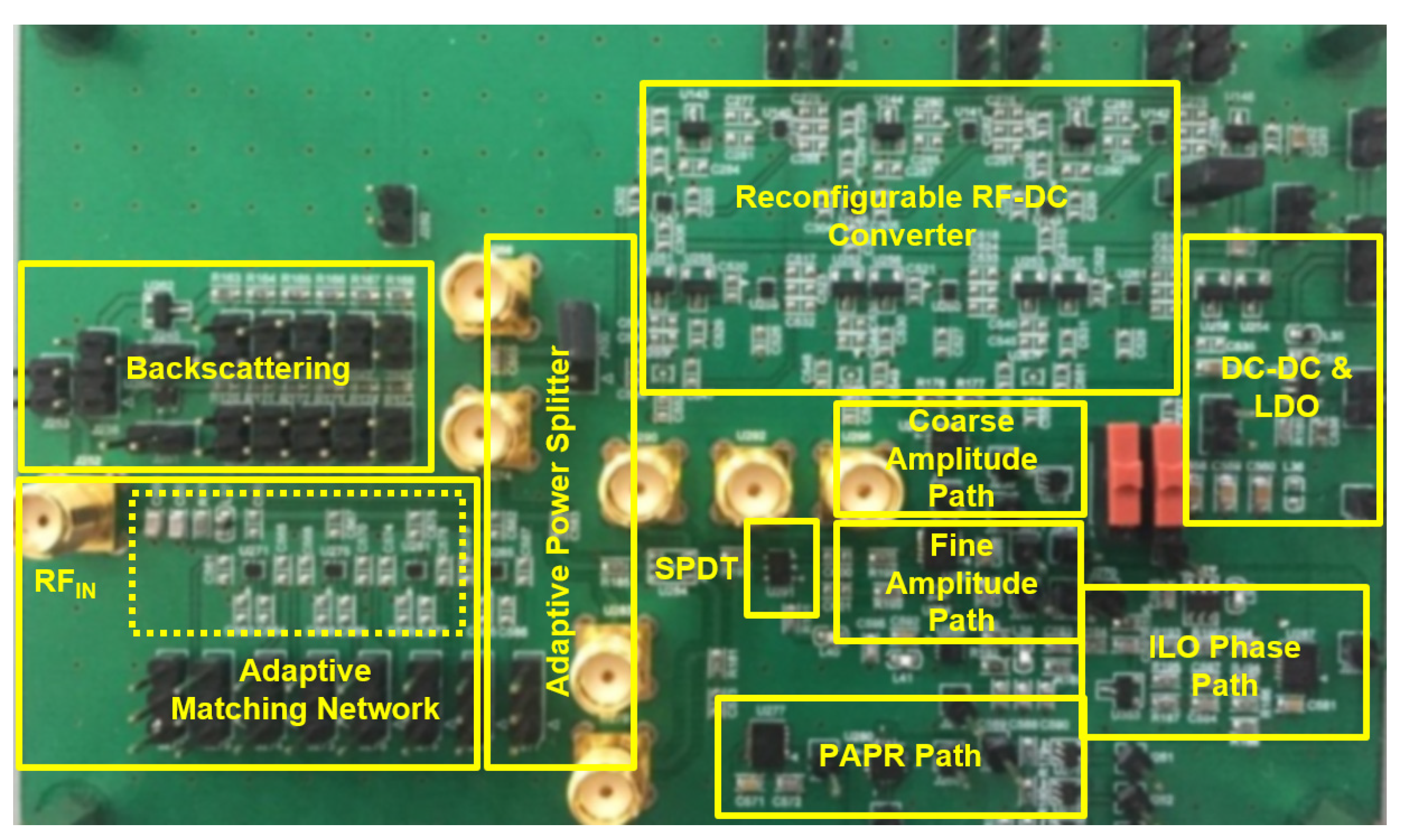
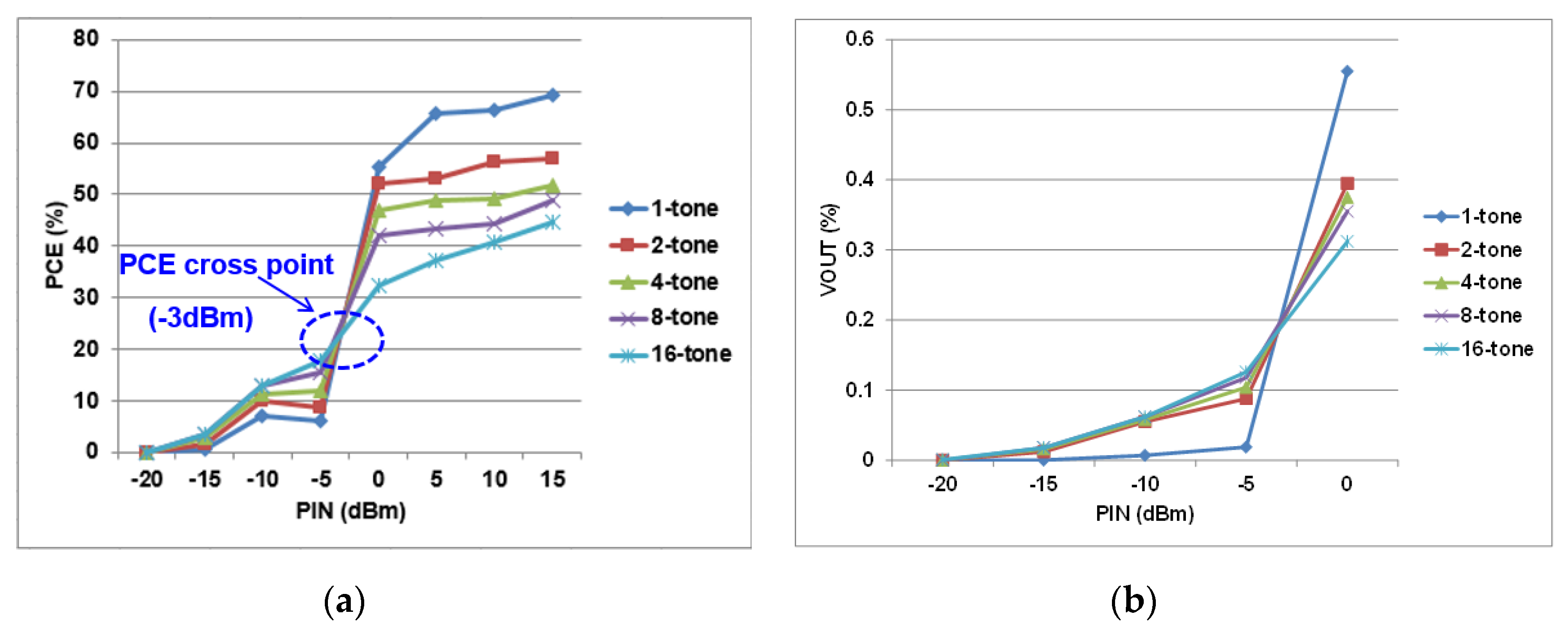
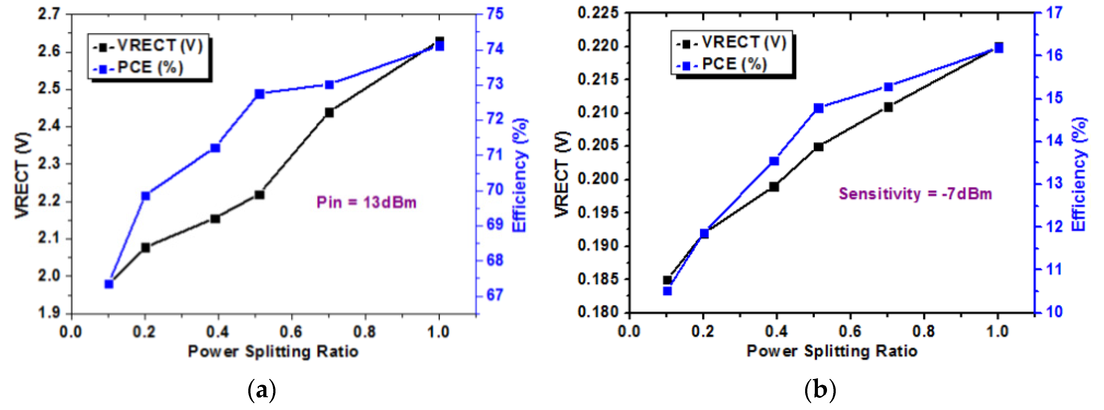
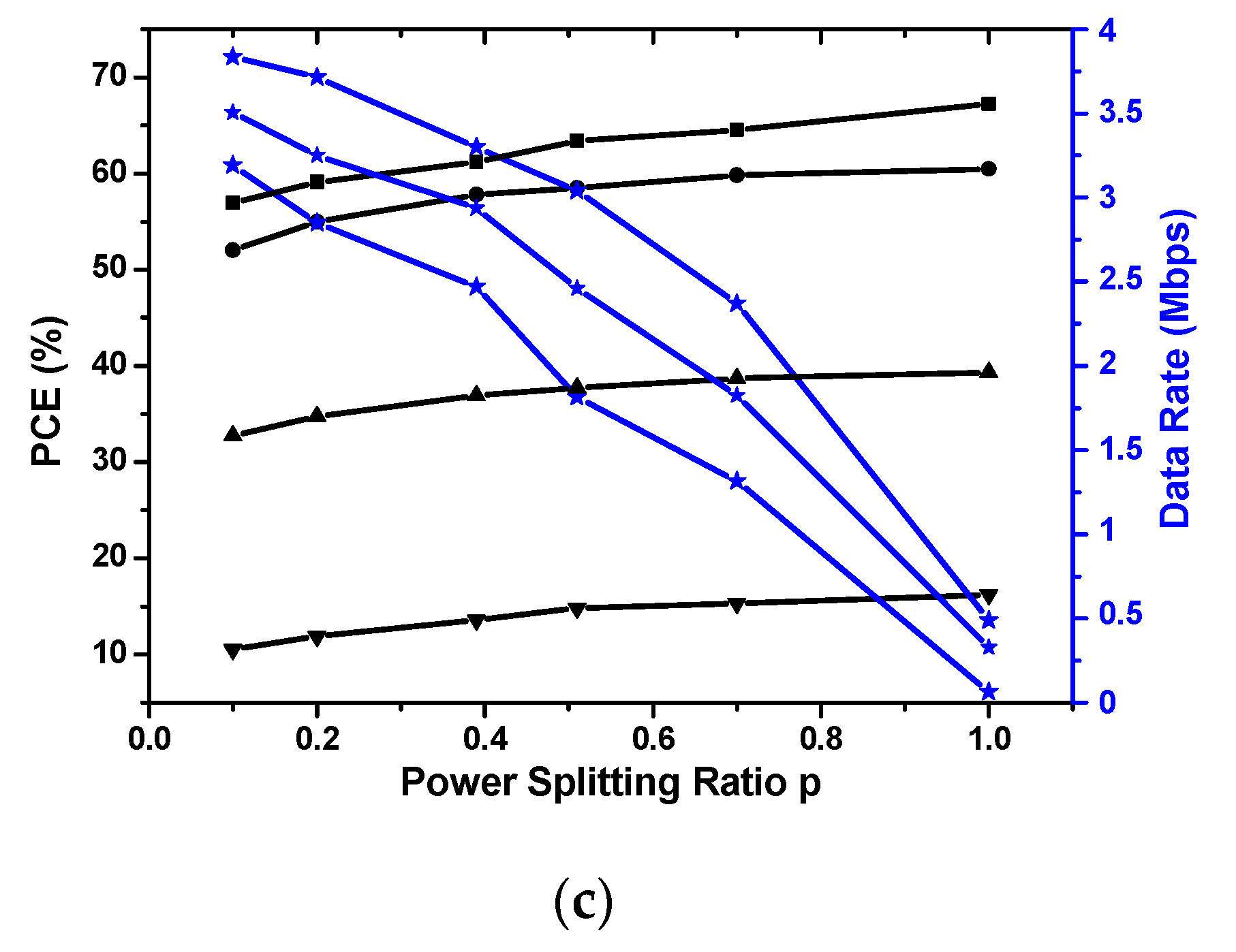
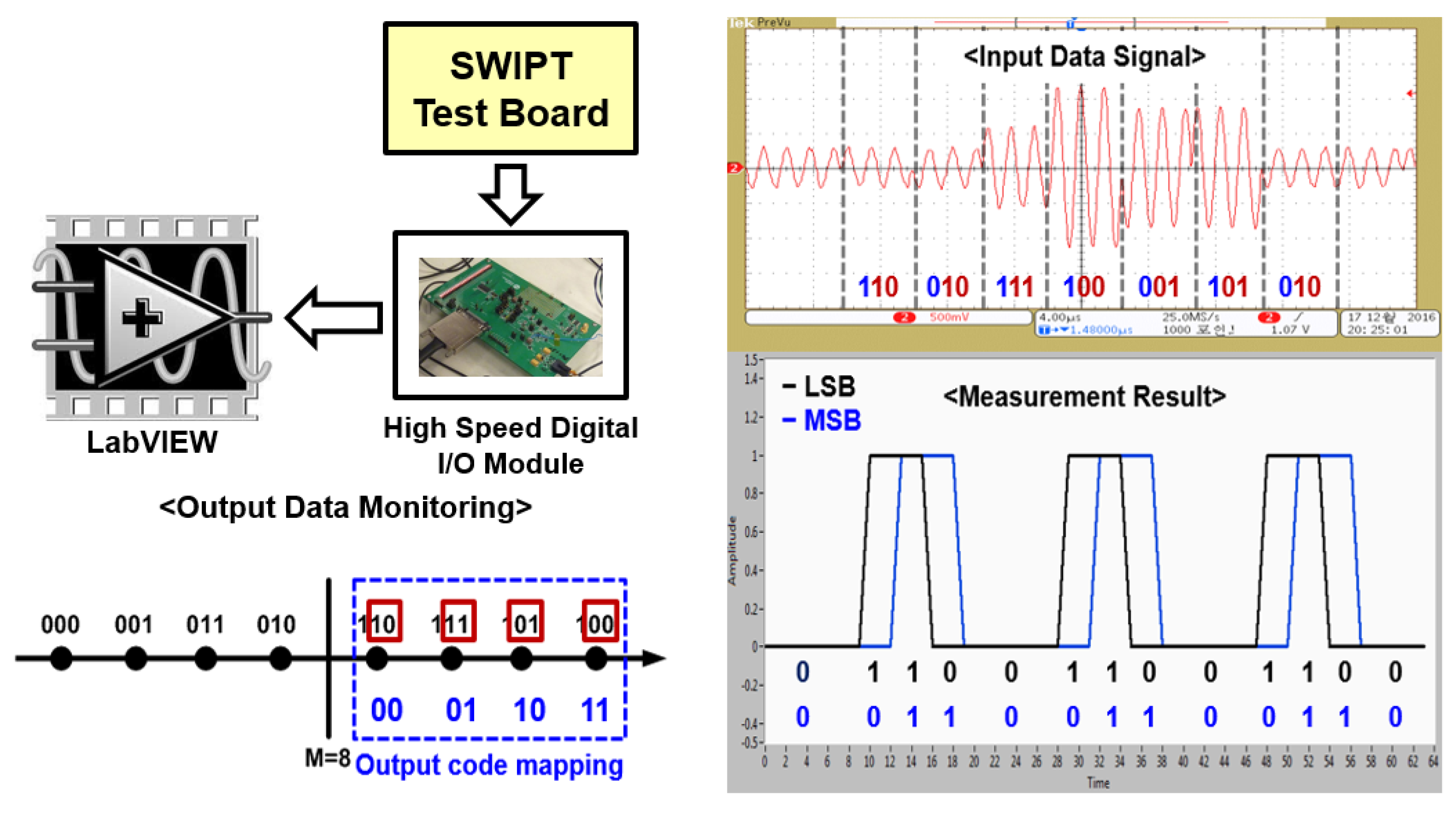
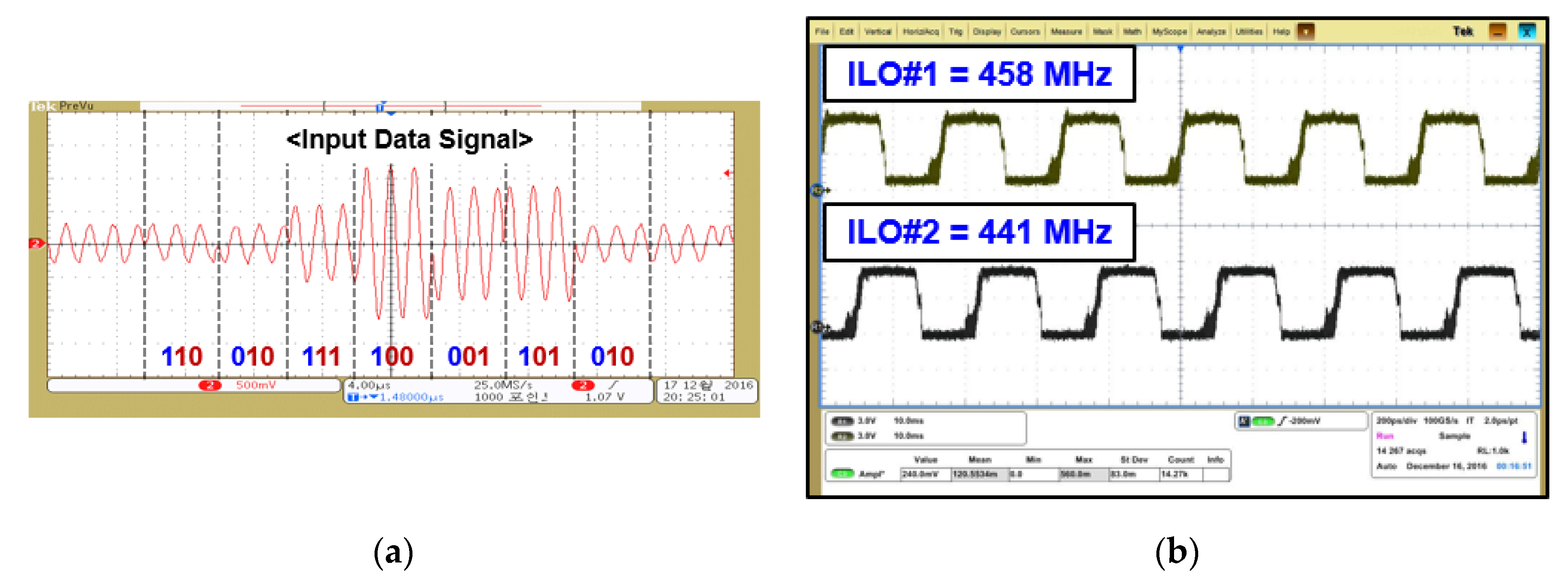
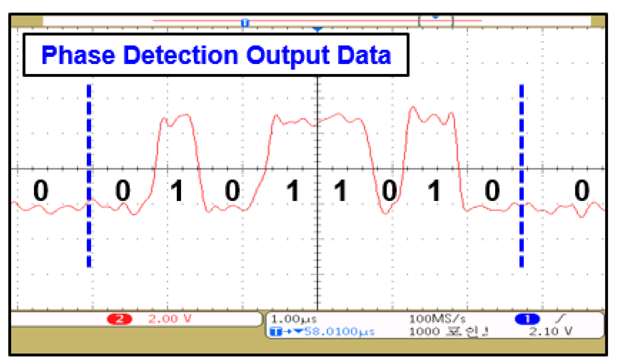
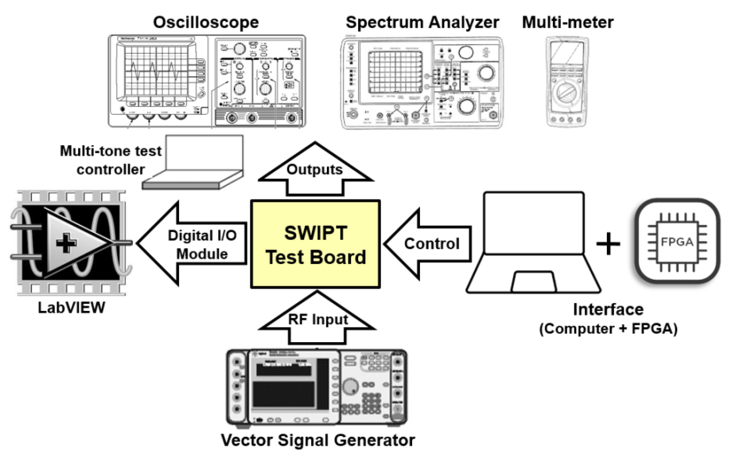
3. Simulation and Experimental Results
4. Conclusions
Author Contributions
Funding
Conflicts of Interest
References
- Paing, T.; Shin, J.; Zane, R.; Popovic, Z. Resistor emulation approach to low-power RF energy harvesting. IEEE Trans. Power Electron. 2008, 23, 1494–1501. [Google Scholar] [CrossRef]
- Vullers, R.J.M.; Schaijk, R.V.; Doms, I.; Hoof, C.V.; Merterns, R. Micro-power energy harvesting. Solid-State Electron. 2009, 53, 684–693. [Google Scholar] [CrossRef]
- Le, T.; Mayaram, K.; Fiez, T. Efficient far-field radio frequency energy harvesting for passively powered sensor networks. IEEE J. Solid-State Circuits 2008, 43, 1287–1302. [Google Scholar] [CrossRef]
- Varshney, L.R. Transporting information and energy simultaneously. In Proceedings of the IEEE International Symposium on Information Theory (ISIT), Toronto, ON, Canada, 6–11 July 2008; pp. 1612–1616. [Google Scholar]
- Grover, P.; Sahai, A. Shannon meets Tesla: Wireless information and power transfer. In Proceedings of the IEEE International Symposium on Information Theory (ISIT), Austin, TX, USA, 13–18 June 2010; pp. 2363–2367. [Google Scholar]
- Fouladgar, A.M.; Simeone, O. On the transfer of information and energy in multi-user systems. IEEE Commun. Lett. 2012, 16, 1733–1736. [Google Scholar] [CrossRef]
- Zhang, R.; Ho, C.K. MIMO broadcasting for simultaneous wireless information and power transfer. IEEE Trans. Wirel. Commun. 2013, 12, 1989–2001. [Google Scholar] [CrossRef]
- Liu, L.; Zhang, R.; Chua, K.-C. Wireless information transfer with opportunistic energy harvesting. IEEE Trans. Wirel. Commun. 2013, 16, 288–300. [Google Scholar] [CrossRef]
- Xu, J.; Liu, L.; Zhang, R. Multiuser MISO beamforming for simultaneous wireless information and power transfer. IEEE Trans. Signal Process. 2014, 62, 4798–4810. [Google Scholar] [CrossRef]
- Zhou, X.; Zhang, R.; Ho, C.K. Wireless information and power transfer: Architecture design and rate-energy tradeoff. IEEE Trans. Commun. 2013, 61, 4754–4767. [Google Scholar] [CrossRef]
- Lu, X.; Wang, P.; Niyato, D.; Kim, D.I.; Han, Z. Wireless networks with RF energy harvesting: A contemporary survey. IEEE Commun. Surv. Tutor. 2015, 17, 757–789. [Google Scholar] [CrossRef]
- Lee, S.; Liu, L.; Zhang, R. Collaborative wireless energy and information transfer in interference channel. IEEE Trans. Wirel. Commun. 2015, 14, 545–557. [Google Scholar] [CrossRef]
- Liu, L.; Zhang, R.; Chua, K.-C. Wireless information and power transfer: A dynamic power splitting approach. IEEE Trans. Commun. 2013, 61, 3990–4001. [Google Scholar] [CrossRef]
- Shi, Q.; Liu, L.; Xu, W.; Zhang, R. Joint transmit beamforming and receive power splitting for MISO SWIPT systems. IEEE Trans. Wirel. Commun. 2014, 13, 3269–3280. [Google Scholar] [CrossRef]
- Timotheou, S.; Krikidis, I.; Zheng, G.; Ottersten, B. Beamforming for MISO interference channels with QoS and RF energy transfer. IEEE Trans. Wirel. Commun. 2014, 13, 2646–2658. [Google Scholar]
- Shi, Q.; Xu, W.; Chang, T.-H.; Wang, Y. Joint beamforming and power splitting for MISO interference channel with SWIPT: An SOCP relaxation and decentralized algorithm. IEEE Trans. Signal Process. 2014, 62, 6194–6208. [Google Scholar] [CrossRef]
- Boshkovska, E.; Ng, D.W.K.; Zlatanov, N.; Schober, R. Practical non-linear energy harvesting model and resource allocation for SWIPT systems. IEEE Commun. Lett. 2015, 19, 2082–2085. [Google Scholar] [CrossRef]
- Kim, D.I.; Moon, J.H.; Park, J.J. New SWIPT using PAPR: How it works. IEEE Wirel. Commun. Lett. 2016, 5, 672–675. [Google Scholar] [CrossRef]
- Park, J.J.; Moon, J.H.; Lee, K.-Y.; Kim, D.I. Adaptive Mode Switching Algorithm for Dual Mode SWIPT with Duty Cycle Operation. In Proceedings of the 2018 IEEE 19th International Workshop on Signal Processing Advances in Wireless Communications (SPAWC), Kalamata, Greece, 25–28 June 2018. [Google Scholar]
- Park, J.J.; Moon, J.H.; Lee, K.-Y.; Kim, D.I. Dual Mode SWIPT: Waveform Design and Transceiver Architecture with Adaptive Mode Switching Policy. In Proceedings of the IEEE VTC ’18 Spring, Porto, Portugal, 3–6 June 2018. [Google Scholar]
- Boaventura, A.S.; Carvalho, N.B. Maximizing DC power in energy harvesting circuits using multisine excitation. In Proceedings of the IEEE MTT-S International Microwave Symposium (MTT), Baltimore, MD, USA, 5–10 June 2011; pp. 1–4. [Google Scholar]
- Clerckx, B.; Bayguzina, E. Waveform design for wireless power transfer. IEEE Trans. Signal Process. 2016, 64, 6313–6328. [Google Scholar] [CrossRef]
- Abbasizadeh, H.; Kim, S.Y.; Nga, T.T.K.; Khan, D.; Oh, S.J.; Kim, S.J.; Kim, K.T.; Kim, D.I.; Lee, K.Y. A 5.2 GHz RF Energy Harvester System Using Reconfigurable Parallel Rectenna. In Proceedings of the 2018 IEEE 61st International Midwest Symposium on Circuits and Systems (MWSCAS), Windsor, ON, Canada, Canada, 5–8 Augest 2018; pp. 1–4. [Google Scholar]
- Wireless Powered Sensor Networks (WPSN) Testbed. Available online: https://youtu.be/qP9fZQX1sDk (accessed on 27 May 2017).
- Choi, K.W.; Kim, D.I. Energy Transmitting Method and Apparatus, Energy Receiving Method, and Receiving Node. U.S. Patent 10411519, 10 September 2019. [Google Scholar]
- Aziz, A.A.; Ginting, L.; Setiawan, D.; Park, J.H.; Tran, N.M.; Yeoo, G.Y.; Kim, D.I.; Choi, K.W. Battery-Less Location Tracking for Internet of Things: Simultaneous Wireless Power Transfer and Positioning. IEEE Int. Things J. 2019, 6, 9147–9164. [Google Scholar] [CrossRef]
- Clerckx, B.; Zhang, R.; Schober, R.; Ng, D.W.K.; Kim, D.I.; Poor, H.V. Fundamentals of wireless information and power transfer: From RF energy harvester models to signal and system designs. IEEE J. Sel. Areas Commun. 2019, 37, 4–33. [Google Scholar] [CrossRef]
- Yedavalli, P.S.; Riihonen, T.; Wang, X.; Rabaey, J.M. Far-field RF wireless power transfer with blind adaptive beamforming for Internet of Things devices. IEEE Access 2017, 5, 1743–1752. [Google Scholar] [CrossRef]
- Choi, K.W.; Aziz, A.A.; Ginting, L.; Setiawan, D.; Park, J.H.; Kim, D.I. Battery-Less Location Tracking Test Demo Video. Available online: http://www.youtube.com/watch?v=zo4Pv6MqmcY (accessed on 31 December 2018).
- Choi, K.W.; Ginting, L.; Aziz, A.A.; Setiawan, D.; Park, J.H.; Hwang, S.I.; Kang, D.S.; Chung, M.Y.; Kim, D.I. Toward Realization of Long-Range Wireless-Powered Sensor Networks. IEEE Wirel. Commun. 2019, 26, 184–192. [Google Scholar] [CrossRef]
- Claessens, S.; Schreurs, D.; Pollin, S. SWIPT with biased ASK modulation and dual-purpose hardware. In Proceedings of the IEEE Wireless Power Transfer Conference (WPTC), Taipei, Taiwan, 10–12 May 2017; pp. 1–4. [Google Scholar]
- Renzo, M.D.; Lu, W. System-level analysis and optimization of cellular networks with simultaneous wireless information and power transfer: Stochastic geometry modeling. IEEE Trans. Veh. Technol. 2017, 66, 2251–2275. [Google Scholar] [CrossRef]
- Varasteh, M.; Rassouli, B.; Joudeh, H.; Clerckx, B. SWIPT signalling over complex AWGN channels with two nonlinear energy harvester models. In Proceedings of the IEEE International Symposium on Information Theory, Vail, CO, USA, 17–22 June 2018. [Google Scholar]
- Lu, X.; Niyato, D.; Jiang, H.; Kim, D.I.; Xiao, Y.; Han, Z. Ambient backscatter assisted wireless powered communications. IEEE Wirel. Commun. 2018, 25, 170–177. [Google Scholar] [CrossRef]
- Yu, H.; Zhang, Y.; Guo, S.; Yang, Y.; Ji, L. Energy Efficiency Maximization for WSNs with Simultaneous Wireless Information and Power Transfer. Sensors 2017, 17, 1906. [Google Scholar] [CrossRef] [PubMed]
- Rajaram, A.; Khan, R.; Tharranetharam, S.; Jayakody, D.N.K.; Dinis, R.; Panic, S. Novel SWIPT Schemes for 5G Wireless Networks. Sensors 2019, 19, 1169. [Google Scholar] [CrossRef] [PubMed]
- Liu, D.; Wen, Z.; Liu, X.; Li, S.; Zou, J. Joint Source-Relay Optimization for MIMO Full-Duplex Bidirectional Wireless Sensor Networks with SWIPT. Sensors 2019, 19, 1827. [Google Scholar] [CrossRef]
- Yang, S.; Lu, G.; Ren, Y. Optimal Power Allocation and Relay Location for DF Energy Harvesting Relaying Sensor Networks. Sensors 2019, 19, 2326. [Google Scholar] [CrossRef] [PubMed]
- Lu, W.; Liu, G.; Si, P.; Zhang, G.; Li, B.; Peng, H. Joint Resource Optimization in Simultaneous Wireless Information and Power Transfer (SWIPT) Enabled Multi-Relay Internet of Things (IoT) System. Sensors 2019, 19, 2536. [Google Scholar] [CrossRef] [PubMed]


| Parameters | Value |
|---|---|
| Technology | PCB level |
| Supply (V) | 3.3/5 |
| Maximum EH efficiency (%) | 69 for 300 Ω load |
| Frequency band (MHz) | 900 (/5.2 GHz using rectenna) |
| Sensitivity (dBm) | −7 dBm |
| Receiver modulation | ASK/BPSK/PAPR |
| Data rate (Mbps) | 1/2.5/4 |
| PAPR support | Yes |
| Implementation | PCB |
| SWIPT support | Yes |
| Power-splitting ratio Transmitter modulation | 0.44 backscatter |
© 2019 by the authors. Licensee MDPI, Basel, Switzerland. This article is an open access article distributed under the terms and conditions of the Creative Commons Attribution (CC BY) license (http://creativecommons.org/licenses/by/4.0/).
Share and Cite
Abbasizadeh, H.; Kim, S.Y.; Samadpoor Rikan, B.; Hejazi, A.; Khan, D.; Pu, Y.G.; Hwang, K.C.; Yang, Y.; Kim, D.I.; Lee, K.-Y. Design of a 900 MHz Dual-Mode SWIPT for Low-Power IoT Devices. Sensors 2019, 19, 4676. https://doi.org/10.3390/s19214676
Abbasizadeh H, Kim SY, Samadpoor Rikan B, Hejazi A, Khan D, Pu YG, Hwang KC, Yang Y, Kim DI, Lee K-Y. Design of a 900 MHz Dual-Mode SWIPT for Low-Power IoT Devices. Sensors. 2019; 19(21):4676. https://doi.org/10.3390/s19214676
Chicago/Turabian StyleAbbasizadeh, Hamed, Sang Yun Kim, Behnam Samadpoor Rikan, Arash Hejazi, Danial Khan, Young Gun Pu, Keum Cheol Hwang, Youngoo Yang, Dong In Kim, and Kang-Yoon Lee. 2019. "Design of a 900 MHz Dual-Mode SWIPT for Low-Power IoT Devices" Sensors 19, no. 21: 4676. https://doi.org/10.3390/s19214676
APA StyleAbbasizadeh, H., Kim, S. Y., Samadpoor Rikan, B., Hejazi, A., Khan, D., Pu, Y. G., Hwang, K. C., Yang, Y., Kim, D. I., & Lee, K.-Y. (2019). Design of a 900 MHz Dual-Mode SWIPT for Low-Power IoT Devices. Sensors, 19(21), 4676. https://doi.org/10.3390/s19214676