Two-Wired Active Spring-Loaded Dry Electrodes for EEG Measurements


Abstract
1. Introduction
2. Design and Implementation
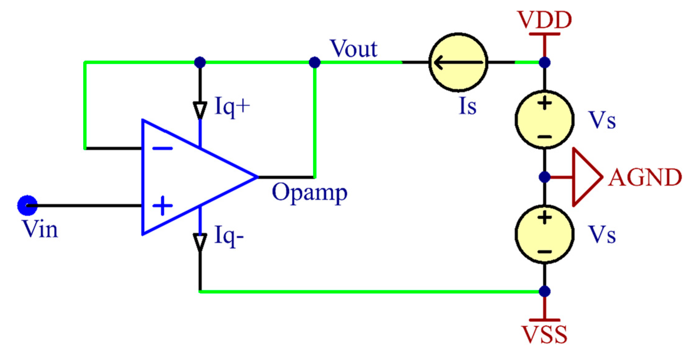
2.1. Two-Wired Active Electrode Design
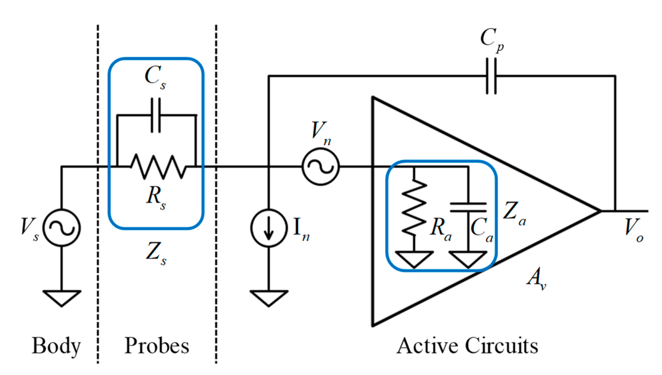
2.2. Electrical Model Analysis and Design Considerations
2.3. Design of Active Dry Electrodes
2.3.1. Spring-Loaded Probes
2.3.2. Amplifier Specifications
2.3.3. Circuit Design and Implementation
3. Evaluation and Experiment
3.1. Noise Characteristics
3.2. Input Capacitance
3.3. Alpha Rhythm Detection Experiment
4. Results
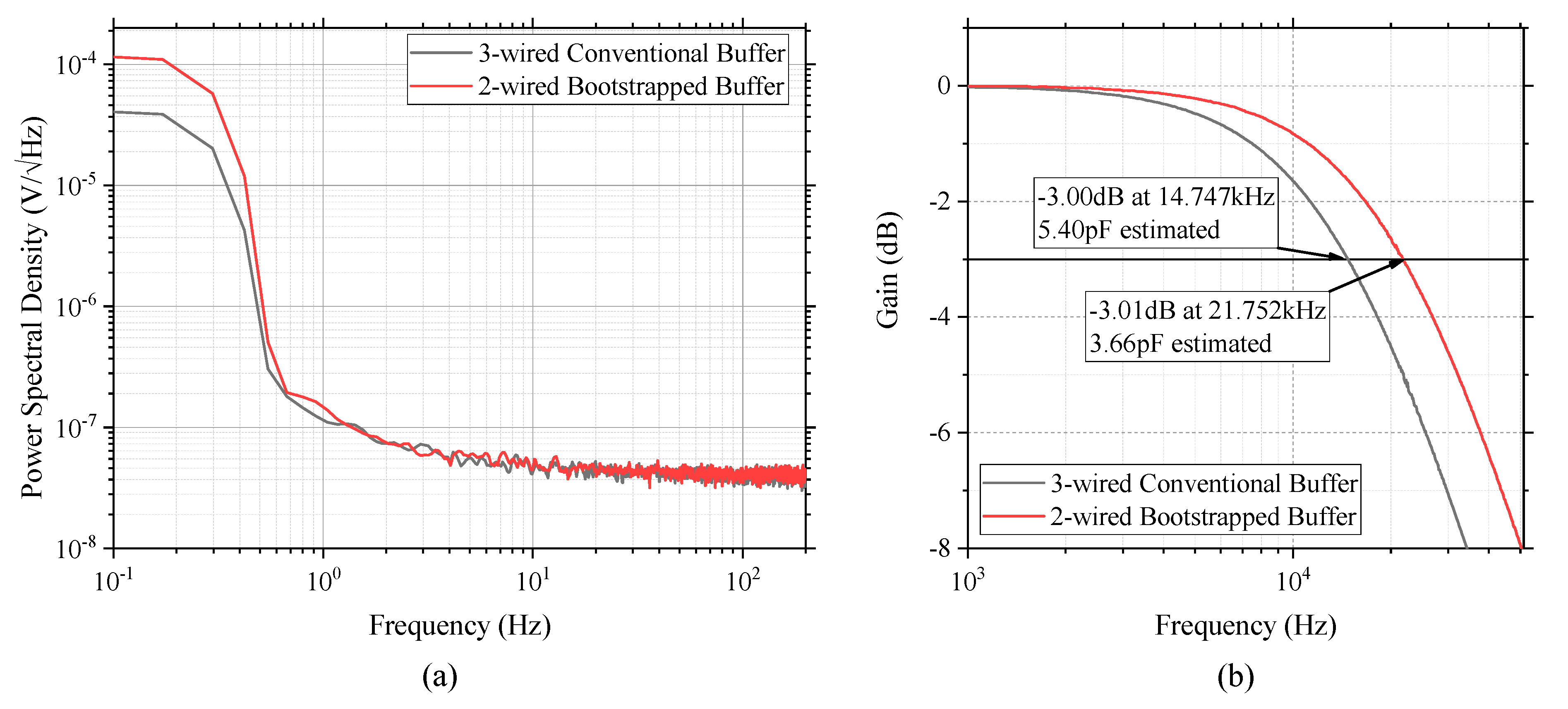
4.1. Noise Power Spectral Density
4.2. Input Capacitance Estimation
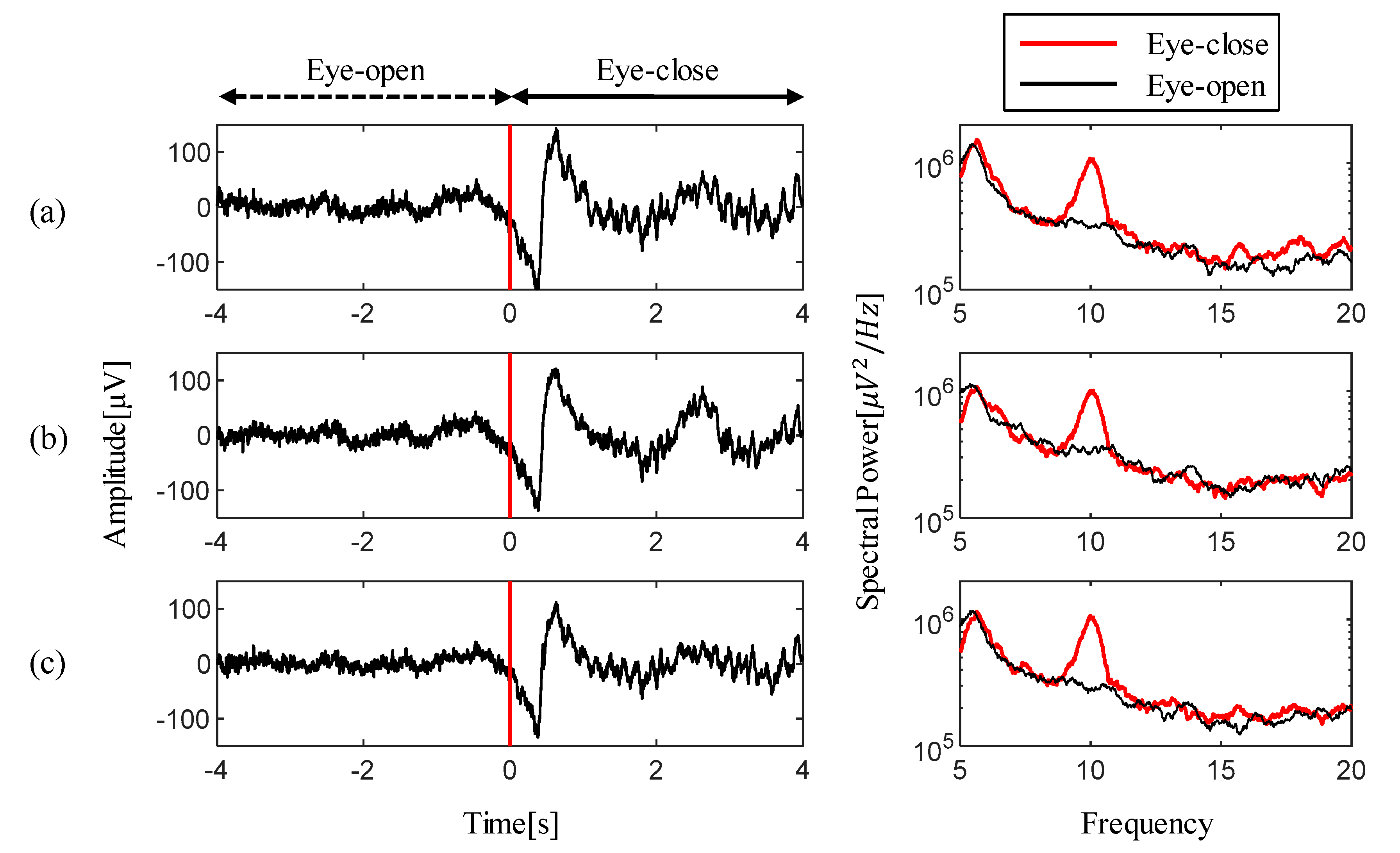
4.3. Experimental Results of Alpha Rhythm Detection
5. Discussion
6. Conclusions
Author Contributions
Funding
Acknowledgments
Conflicts of Interest
References
- Lopez-Gordo, M.A.; Sanchez-Morillo, D.; Valle, F.P. Dry EEG Electrodes. Sensors 2014, 14, 12847–12870. [Google Scholar] [CrossRef] [PubMed]
- Smith, S.J.M. EEG in the diagnosis, classification, and management of patients with epilepsy. J. Neurol. Neurosurg. Psychiatry 2005, 76, 2–7. [Google Scholar] [CrossRef] [PubMed]
- Nicolas-Alonso, L.F.; Gomez-Gil, J. Brain Computer Interfaces—A Review. Sensors 2012, 12, 1211–1279. [Google Scholar] [CrossRef] [PubMed]
- Millán, J.D.R.; Rupp, R.; Müller-Putz, G.R.; Murray-Smith, R.; Giugliemma, C.; Tangermann, M.; Vidaurre, C.; Cincotti, F.; Kübler, A.; Leeb, R.; et al. Combining Brain–Computer Interfaces and Assistive Technologies: State-of-the-Art and Challenges. Front Neurosci. 2010, 4. [Google Scholar] [CrossRef]
- Ren, L.; Liu, B.; Zhou, W.; Jiang, L. A Mini Review of Microneedle Array Electrode for Bio-Signal Recording: A Review. IEEE Sens. J. 2019, 1. [Google Scholar] [CrossRef]
- Yao, S.; Zhu, Y. Nanomaterial-Enabled Dry Electrodes for Electrophysiological Sensing: A Review. JOM 2016, 68, 1145–1155. [Google Scholar] [CrossRef]
- Griss, P.; Enoksson, P.; Tolvanen-Laakso, H.K.; Merilainen, P.; Ollmar, S.; Stemme, G. Micromachined electrodes for biopotential measurements. J. Microelectromechanical Syst. 2001, 10, 10–16. [Google Scholar] [CrossRef]
- Dias, N.S.; Carmo, J.P.; da Silva, A.F.; Mendes, P.M.; Correia, J.H. New dry electrodes based on iridium oxide (IrO) for non-invasive biopotential recordings and stimulation. Sens. Actuators A Phys. 2010, 164, 28–34. [Google Scholar] [CrossRef]
- O’Mahony, C.; Pini, F.; Blake, A.; Webster, C.; O’Brien, J.; McCarthy, K.G. Microneedle-based electrodes with integrated through-silicon via for biopotential recording. Sens. Actuators A Phys. 2012, 186, 130–136. [Google Scholar] [CrossRef]
- Ruffini, G.; Dunne, S.; Fuentemilla, L.; Grau, C.; Farrés, E.; Marco-Pallarés, J.; Watts, P.C.P.; Silva, S.R.P. First human trials of a dry electrophysiology sensor using a carbon nanotube array interface. Sens. Actuators A Phys. 2008, 144, 275–279. [Google Scholar] [CrossRef]
- Song, Y.; Li, P.; Li, M.; Li, H.; Li, C.; Sun, D.; Yang, B. Fabrication of chitosan/Au-TiO2 nanotube-based dry electrodes for electroencephalography recording. Mater. Sci. Eng. C 2017, 79, 740–747. [Google Scholar] [CrossRef] [PubMed]
- Zhang, H.; Pei, W.; Chen, Y.; Guo, X.; Wu, X.; Yang, X.; Chen, H. A Motion Interference-Insensitive Flexible Dry Electrode. IEEE Trans. Biomed. Eng. 2016, 63, 1136–1144. [Google Scholar] [CrossRef] [PubMed]
- Chi, Y.M.; Jung, T.P.; Cauwenberghs, G. Dry-Contact and Noncontact Biopotential Electrodes: Methodological Review. IEEE Rev. Biomed. Eng. 2010, 3, 106–119. [Google Scholar] [CrossRef] [PubMed]
- Sullivan, T.J.; Deiss, S.R.; Cauwenberghs, G. A Low-Noise, Non-Contact EEG/ECG Sensor. In Proceedings of the 2007 IEEE Biomedical Circuits and Systems Conference, Montreal, QC, Canada, 27–30 November 2007; pp. 154–157. [Google Scholar]
- Chi, Y.M.; Maier, C.; Cauwenberghs, G. Ultra-High Input Impedance, Low Noise Integrated Amplifier for Noncontact Biopotential Sensing. IEEE J. Emerg. Sel. Top. Circuits Syst. 2011, 1, 526–535. [Google Scholar] [CrossRef]
- Chi, Y.M.; Wang, Y.; Wang, Y.; Maier, C.; Jung, T.; Cauwenberghs, G. Dry and Noncontact EEG Sensors for Mobile Brain–Computer Interfaces. IEEE Trans. Neural Syst. Rehabil. Eng. 2012, 20, 228–235. [Google Scholar] [CrossRef] [PubMed]
- Baek, H.J.; Kim, H.S.; Heo, J.; Lim, Y.G.; Park, K.S. Brain–computer interfaces using capacitive measurement of visual or auditory steady-state responses. J. Neural Eng. 2013, 10, 024001. [Google Scholar] [CrossRef] [PubMed]
- Lee, S.M.; Kim, J.H.; Byeon, H.J.; Choi, Y.Y.; Park, K.S.; Lee, S.-H. A capacitive, biocompatible and adhesive electrode for long-term and cap-free monitoring of EEG signals. J. Neural Eng. 2013, 10, 036006. [Google Scholar] [CrossRef]
- Lee, S.M.; Kim, J.H.; Park, C.; Hwang, J.; Hong, J.S.; Lee, K.H.; Lee, S.H. Self-Adhesive and Capacitive Carbon Nanotube-Based Electrode to Record Electroencephalograph Signals from the Hairy Scalp. IEEE Trans. Biomed. Eng. 2016, 63, 138–147. [Google Scholar] [CrossRef]
- Baek, H.J.; Lee, H.J.; Lim, Y.G.; Park, K.S. Comparison of pre-amplifier topologies for use in brain-computer interface with capacitively-coupled EEG electrodes. Biomed. Eng. Lett. 2013, 3, 158–169. [Google Scholar] [CrossRef]
- Liao, L.-D.; Wang, I.-J.; Chen, S.-F.; Chang, J.-Y.; Lin, C.-T. Design, Fabrication and Experimental Validation of a Novel Dry-Contact Sensor for Measuring Electroencephalography Signals without Skin Preparation. Sensors 2011, 11, 5819–5834. [Google Scholar] [CrossRef]
- Grozea, C.; Voinescu, C.D.; Fazli, S. Bristle-sensors—Low-cost flexible passive dry EEG electrodes for neurofeedback and BCI applications. J. Neural Eng. 2011, 8, 025008. [Google Scholar] [CrossRef] [PubMed]
- Gao, K.; Yang, H.; Liao, L.; Jiang, C.; Zhao, N.; Wang, X.; Li, X.; Yang, B.; Liu, J. A Novel Bristle-shaped Semi-dry Electrode with Low Contact Impedance and Ease of Use Features for EEG Signal Measurement. IEEE Trans. Biomed. Eng. 2019, 1. [Google Scholar] [CrossRef] [PubMed]
- Chen, Y.-H.; de Beeck, M.O.; Vanderheyden, L.; Carrette, E.; Mihajlović, V.; Vanstreels, K.; Grundlehner, B.; Gadeyne, S.; Boon, P.; Van Hoof, C. Soft, Comfortable Polymer Dry Electrodes for High Quality ECG and EEG Recording. Sensors 2014, 14, 23758–23780. [Google Scholar] [CrossRef] [PubMed]
- Fiedler, P.; Mühle, R.; Griebel, S.; Pedrosa, P.; Fonseca, C.; Vaz, F.; Zanow, F.; Haueisen, J. Contact Pressure and Flexibility of Multipin Dry EEG Electrodes. IEEE Trans. Neural Syst. Rehabil. Eng. 2018, 26, 750–757. [Google Scholar] [CrossRef] [PubMed]
- Krachunov, S.; Casson, A.J. 3D Printed Dry EEG Electrodes. Sensors 2016, 16, 1635. [Google Scholar] [CrossRef]
- Li, G.; Zhang, D.; Wang, S.; Duan, Y.Y. Novel passive ceramic based semi-dry electrodes for recording electroencephalography signals from the hairy scalp. Sens. Actuators B Chem. 2016, 237, 167–178. [Google Scholar] [CrossRef]
- Xu, J.; Mitra, S.; Hoof, C.V.; Yazicioglu, R.F.; Makinwa, K.A.A. Active Electrodes for Wearable EEG Acquisition: Review and Electronics Design Methodology. IEEE Rev. Biomed. Eng. 2017, 10, 187–198. [Google Scholar] [CrossRef]
- Huang, Y.J.; Wu, C.Y.; Wong, A.M.K.; Lin, B.S. Novel Active Comb-Shaped Dry Electrode for EEG Measurement in Hairy Site. IEEE Trans. Biomed. Eng. 2015, 62, 256–263. [Google Scholar] [CrossRef]
- Guerrero, F.N.; Spinelli, E.M. A Two-Wired Ultra-High Input Impedance Active Electrode. IEEE Trans. Biomed. Circuits Syst. 2018, 12, 437–445. [Google Scholar] [CrossRef]
- Guermandi, M.; Cardu, R.; Scarselli, E.F.; Guerrieri, R. Active Electrode IC for EEG and Electrical Impedance Tomography with Continuous Monitoring of Contact Impedance. IEEE Trans. Biomed. Circuits Syst. 2015, 9, 21–33. [Google Scholar] [CrossRef]
- Pourahmad, A.; Dehghani, R. Two-Wired Current Modulator Active Electrode for Ambulatory Biosignal Recording. IEEE Trans. Biomed. Circuits Syst. 2019, 13, 15–25. [Google Scholar] [CrossRef] [PubMed]
- Degen, T.; Torrent, S.; Jackel, H. Low-Noise Two-Wired Buffer Electrodes for Bioelectric Amplifiers. IEEE Trans. Biomed. Eng. 2007, 54, 1328–1332. [Google Scholar] [CrossRef] [PubMed]
- An Applications Guide for Op Amps. Available online: http://www.ti.com/lit/an/snoa621c/snoa621c.pdf (accessed on 17 October 2019).
- Lányi, S. The noise of input stages with low parasitic capacitance. Meas. Sci. Technol. 2001, 12, 1456. [Google Scholar] [CrossRef]
- Lanyi, S.; Pisani, M. A high-input-impedance buffer. IEEE Trans. Circuits Syst. I Fundam. Theory Appl. 2002, 49, 1209–1211. [Google Scholar] [CrossRef]
- Noise Analysis in Operational Amplifier Circuits. Available online: http://www.ti.com/lit/an/slva043b/slva043b.pdf (accessed on 17 October 2019).
- OPA378 Datasheet. Available online: http://www.ti.com/lit/ds/symlink/opa378.pdf (accessed on 5 September 2019).
- Low Noise Signal Conditioning for Sensor-Based Circuits. Available online: https://www.analog.com/media/en/technical-documentation/technical-articles/MS-2066.pdf (accessed on 17 October 2019).
- To Chop or Auto-Zero: That Is the Question. Available online: https://www.analog.com/media/en/technical-documentation/technical-articles/MS-2062.pdf (accessed on 17 October 2019).
- Degen, T.; Jackel, H. A pseudodifferential amplifier for bioelectric events with DC-offset compensation using two-wired amplifying electrodes. IEEE Trans. Biomed. Eng. 2006, 53, 300–310. [Google Scholar] [CrossRef]
- REF200 Datasheet. Available online: http://www.ti.com/lit/ds/symlink/ref200.pdf (accessed on 5 September 2019).
- Measure the Input Capacitance of an Op Amp. Available online: https://pdfserv.maximintegrated.com/en/an/AN5086.pdf (accessed on 17 October 2019).
- Lee, S.; Shin, Y.; Kumar, A.; Kim, M.; Lee, H. Dry Electrode-Based Fully Isolated EEG/fNIRS Hybrid Brain-Monitoring System. IEEE Trans. Biomed. Eng. 2019, 66, 1055–1068. [Google Scholar] [CrossRef]
- Achermann, P.; Dijk, D.-J.; Brunner, D.P.; Borbély, A.A. A model of human sleep homeostasis based on EEG slow-wave activity: Quantitative comparison of data and simulations. Brain Res. Bull. 1993, 31, 97–113. [Google Scholar] [CrossRef]
- Design Trade-Offs for Single-Supply Op Amps. Available online: https://pdfserv.maximintegrated.com/en/an/AN656.pdf (accessed on 17 October 2019).


| Electrical Parameters | Characteristics |
|---|---|
| Voltage noise | 0.4 μVPP at 0.1–10 Hz |
| Noise power spectral density | 20 nV/ at 1 kHz |
| Offset voltage and offset drift | 20 μV and 0.1 μV/℃ |
| Input capacitance | 5 pF with common mode |
| Input bias current | ± 150 pA, max. 550 pA |
| Power supply voltage range | 2.2–5.5 V (rail-to-rail) |
| Quiescent current | 125 μA, max. 150 μV |
| 2-wired Active vs. Passive (ρ2) | 3-wired Active vs. Passive (ρ3) | 2-wired Active vs. 3-wired Active (ρ23) |
|---|---|---|
| 0.8536 | 0.8657 | 0.7854 |
© 2019 by the authors. Licensee MDPI, Basel, Switzerland. This article is an open access article distributed under the terms and conditions of the Creative Commons Attribution (CC BY) license (http://creativecommons.org/licenses/by/4.0/).
Share and Cite
Lee, S.; Shin, Y.; Kumar, A.; Kim, K.; Lee, H.-N. Two-Wired Active Spring-Loaded Dry Electrodes for EEG Measurements. Sensors 2019, 19, 4572. https://doi.org/10.3390/s19204572
Lee S, Shin Y, Kumar A, Kim K, Lee H-N. Two-Wired Active Spring-Loaded Dry Electrodes for EEG Measurements. Sensors. 2019; 19(20):4572. https://doi.org/10.3390/s19204572
Chicago/Turabian StyleLee, Seungchan, Younghak Shin, Anil Kumar, Kiseon Kim, and Heung-No Lee. 2019. "Two-Wired Active Spring-Loaded Dry Electrodes for EEG Measurements" Sensors 19, no. 20: 4572. https://doi.org/10.3390/s19204572
APA StyleLee, S., Shin, Y., Kumar, A., Kim, K., & Lee, H.-N. (2019). Two-Wired Active Spring-Loaded Dry Electrodes for EEG Measurements. Sensors, 19(20), 4572. https://doi.org/10.3390/s19204572