Article

On-Chip Non-Dispersive Infrared CO2 Sensor Based on an Integrating Cylinder

1
Photonics Research Group, INTEC, Ghent University-imec, Technologiepark 126, 9052 Gent, Belgium
2
Center for Nano- and Biophotonics, Ghent University, 9000 Gent, Belgium
3
Melexis Technologies NV, Transportstraat 1, 3980 Tessenderlo, Belgium
*
Author to whom correspondence should be addressed.
This paper is an extended version of our paper published in: Jia, X.; Roelkens, G.; Baets, R.; Roels, J. A miniaturized non-dispersive infrared CO2 sensor based on a 2D integrating cylinder. Optical Sensors. In Proceedings of the Embedded Technologies Expo & Conference, San Jose, CA, USA, 25–27 June 2019.
Sensors 2019, 19(19), 4260; https://doi.org/10.3390/s19194260
Submission received: 14 August 2019 / Revised: 26 September 2019 / Accepted: 27 September 2019 / Published: 30 September 2019
(This article belongs to the Section Optical Sensors)

Abstract

:
In this paper, we propose a novel, miniaturized non-dispersive infrared (NDIR) CO2 sensor implemented on a silicon chip. The sensor has a simple structure, consisting of a hollow metallic cylindrical cavity along with access waveguides. A detailed analysis of the proposed sensor is presented. Simulation with 3D ray tracing shows that an integrating cylinder with 4 mm diameter gives an equivalent optical path length of 3.5 cm. The sensor is fabricated using Deep Reactive Ion Etching (DRIE) and wafer bonding. The fabricated sensor was evaluated by performing a CO2 concentration measurement, showing a limit of detection of ∼100 ppm. The response time of the sensor is only ∼2.8 s, due to its small footprint. The use of DRIE-based waveguide structures enables mass fabrication, as well as the potential co-integration of flip-chip integrated midIR light-emitting diodes (LEDs) and photodetectors, resulting in a compact, low-power, and low-cost NDIR CO2 sensor.

1. Introduction

CO2 gas sensing is receiving increasing attention in both industry and academia, due to its widespread applications such as in air-quality monitoring [1], greenhouse farming [2] and industrial process control [3]. The European advanced CO2 sensor market is expected to grow to 3.6 billion dollars by 2021 with a compound annual growth rate of 14.6% [4], which is a huge market for low-cost, miniaturized CO2 sensors. Moreover, the European Union introduced a gradual ban on the usage of fluorinated gases in mobile air conditioning systems (MAC) for environmental and fire safety reasons [5]. CO2 is considered to be a suitable substitute for MAC refrigerants, as its global warming potential (GWP) is several thousand times smaller than that of fluorinated gases [6]. However, safety concerns about potential leakage of CO2, e.g., on board of a car, arise. As the vehicle cabin is a small-volume, relatively confined environment, a trivial leakage of CO2 on board may lead to fatal situations for the driver and the passengers. It has been shown that the CO2 concentration in a car can increase up to 7% within one minute when a sudden leak happens [7]. Although CO2 is not classified as a toxic gas, exposure to elevated CO2 concentration levels can produce a variety of health problems. Concentrations of 7% can cause headache, dizziness, visual disturbances, and even unconsciousness within a few minutes [8]. This can be very dangerous for the people on board as well as for the traffic. CO2-related symptoms can also occur at much lower concentration levels. Studies have shown that at concentrations as low as 1000 ppm (only about 3 times higher than the typical outdoor concentration), an exposure time of 2.5 h can lead to decline in cognitive abilities and basic activity level [9,10]. The colorless and odorless nature of CO2 gas make it practically impossible to detect with the human senses, and therefore sensors are needed to constantly monitor the CO2 concentration in order to remove the safety concerns. Different applications may differ in their requirements of sensor performance such as detection limit, accuracy and response time. For air-quality monitoring and greenhouse farming, a detection limit and accuracy of sub-100 ppm is needed, for leak detection in mobile air conditioning systems, a detection limit of a few thousands ppm is sufficient, yet a fast response time is essential since the CO2 concentration in the cabin increases quite rapidly as previously discussed. In this work, we are targeting both applications by demonstrating a fast sensor with low limit of detection.
The existing CO2 sensors can be categorized into 2 types: electrochemical sensors and non-dispersive infrared (NDIR) sensors. Electrochemical sensors measure the CO2 concentration by measuring a change in the electrical properties of materials induced by the CO2 adsorption. They have the advantage of being low cost and compact [11,12,13,14]. However, electrochemical sensors suffer from short-term stability, low durability and cross-response to other gases (e.g., water vapor) [15,16]. In contrast, NDIR sensors offer long-term stability, high accuracy and high gas specificity [17], and this method is more favorable compared to electrochemical sensors as CO2 is an inert gas and has minimal electrochemical response. Typically, NDIR CO2 sensors use the strong absorption of CO2 around 4.25 µm, a wavelength range where no other common molecules absorb, thereby avoiding cross-sensitivity issues. Due to these advantages, 83% of the European advanced CO2 sensor market uses NDIR sensors [4]. However, NDIR sensors tend to be bulky as a long (typically several cm) interaction length is required to achieve ppm level detection [18,19], and they are also expensive as they are based on discrete co-assembled optical elements, which limit their application in price and size sensitive markets. Intense efforts have been made to miniaturize NDIR sensors, mainly by optimizing the optics design [20,21,22,23], or by using optical cavities [24,25]. Furthermore, pre-concentrators have been employed in NDIR sensors to effectively enhance the CO2 concentration and thus decrease the required optical path length [26,27].
In this paper, we present a continuation and extension of our work [28] published in Optical Sensors and Sensing Congress—OSA 2019. This extension demonstrates an NDIR CO2 sensor based on an integrating cylinder implemented on a silicon substrate. The sensor consists of a hollow gold-coated cylindrical cavity along with hollow metallic waveguides, one at the input and two at the output, realized by Deep Reactive Ion Etching (DRIE) and wafer bonding. The design of the sensor is inspired by the concept of an integrating sphere. In an integrating sphere, the incident light experiences multiple reflections before it reaches the detector, which effectively increase the optical path length. Here, we have taken the concept of the integrating sphere into the world of silicon photonics, by realizing it using MEMS-compatible fabrication technologies. The use of an integrating cylinder allows for a compact sensor with a long interaction length. Simulation with 3D ray tracing shows the sensor has an equivalent path length of ∼3.5 cm, with a footprint of only 6 × 6 mm2. CO2 sensing experiments are carried out on the sensor, showing a detection limit of ∼100 ppm. Moreover, the sensor shows a response time of only 2.8 s. The fast response of the sensor is due to its small size for gas to diffuse.

2. NDIR Working Principle

Many gas molecules have specific vibrational and rotational absorption lines in the mid-IR range [29], and this unique absorption is often used to detect their presence and concentration. It is well known that CO2 has a strong absorption band around a wavelength of 4.25 µm, and the absorption is quantitatively described by the well-known Beer–Lambert law (for monochromatic light):
I = I 0 e ϵ c L
where I and I 0 are the light intensity at the output and input, respectively, ϵ is the molar attenuation coefficient, c is the CO2 concentration, and L is the interaction length. The transmission from the source to the detector is thus given by:
T = I I o = e ϵ c L
One can see that for a fixed sensor configuration(fixed L), the transmission is related to the CO2 concentration, thus by measuring the transmission change one can deduce the CO2 concentration in the gas sample. The structure of a typical NDIR CO2 sensor is shown in Figure 1, which consists of four elements: an optical source at and around 4.25 µm, a gas chamber, optical bandpass filters, and detectors. The active filter is typically centered at 4.25 µm where CO2 has strong absorption (active channel), and the reference filter is typically centered at 3.9 µm, where no common gas molecules absorb (reference channel). During a CO2 sensing measurement, the signal at the active channel ( I A ) will experience exponential decay due to CO2 absorption, while the signal in the reference channel ( I R ) will not change. Thus, by comparing the signal in both channels the CO2 concentration in the target gas can be calculated. The presence of the reference channel is to eliminate the impact of source fluctuation, assuming it has the same influence on both the active and reference channels.

3. Sensor Design

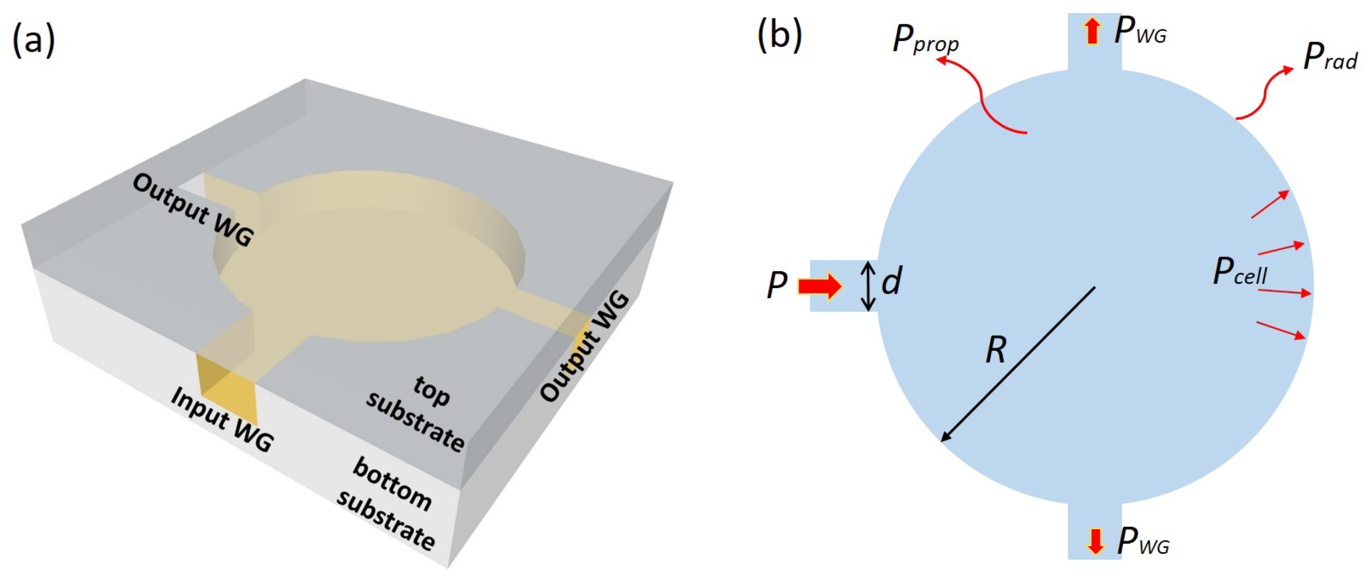
Figure 2a shows the 3D schematic of the sensor proposed in this work. It consists of a gold-coated hollow cylindrical cavity with one input waveguide and two output waveguides. The gold-coated inner surface acts as a reflector to confine light inside the cavity, the input waveguide is used to launch incident light into the integrating cylinder and the output waveguides are used to extract the light signal from the cavity and couple it to detectors. With external optical filters, the two output waveguides can act as active channel and reference channel for the sensor. On the cavity sidewall, random roughness is deliberately applied to scatter the incident light into random directions. As the incident light experiences multiple reflections before reaching the detector, a long effective path length can be achieved inside the cylindrical cavity.
In the cavity slab, the incident light is just specularly reflected on the parallel gold-coated top and bottom surfaces. Therefore, the analysis of the integrating cylinder can be reduced from 3D to 2D, as shown in Figure 2b. When we assume that the light incident on the sidewall is reflected in a random direction, the average distance the light beam travels between two consecutive reflections, is given by [30]:
L a v g = 4 π · R
with R being the radius of the circle. When incident light with power P is coupled into the cavity through the input waveguide, at steady state, there is a uniform distribution of energy in the cavity. When we define the power incident on the sidewall as P c e l l , then the total input power P coupled to the cavity can be “lost” through the extraction loss from each of the access waveguides, the radiation loss/absorption upon incidence on the sidewall and the propagation loss through the cavity slab, given by
P W G = β P c e l l
P r a d = γ P c e l l
P p r o p = η P c e l l
respectively [31]. β is the extraction coefficient from the access waveguides, and is given by the ratio of the width of the waveguide (d) and the circumference of the circle:
β = d 2 π R
γ is the fraction of power radiated/absorbed at the sidewall, related to the reflectivity ρ of the sidewall mirror:
γ = 1 ρ
η is the loss of the light propagating in the cavity slab between two consecutive reflections on the sidewalls, whether by the waveguide loss α p r o p or by the CO2 absorption, characterized by the absorption coefficient α C O 2 :
η = 1 exp ( L a v g ( α p r o p + α C O 2 ) ) L a v g ( α p r o p + α C O 2 )
Due to energy conservation, the input power equals the summation of all losses:
P = 3 P W G + P p r o p + P r a d
From Equations (4)–(6) and Equation (10) we can deduce a relationship between the fraction of power coupled to the waveguide P W G and the input power P:
P W G = β 3 β + γ + η P
Thus, the transmission from the input to the output waveguide is given by:
T = P W G P = β 3 β + γ + η = β 3 β + 1 ρ + 4 π R ( α p r o p + α C O 2 )
where the term 4 π R is the average distance between two consecutive reflections as shown in Equation (3). We define the sensitivity S of the sensor to be the transmission change induced by CO2 absorption, a quantity that can be calculated by taking the partial derivative of the transmission T w.r.t α C O 2 :
S = T α C O 2 = 2 π β R ( 3 β + 1 ρ + 4 π R ( α p r o p + α C O 2 ) ) 2
which has a maximum as a function of R (assuming a fixed β ) when
3 β + 1 ρ = 4 π R ( α p r o p + α C O 2 )
The term on the left-hand side of Equation (14) can be considered to be the “extraction” from the cavity sidewall, which consists of extraction by the waveguides and the radiation/absorption loss from the sidewalls as the reflectivity ρ is less than 1. The term on the right-hand side is the absorption in the slab of the cavity, which consists of waveguide loss and CO2 absorption loss. It can be seen from Equation (13) that the sensor is most sensitive when the “extraction” equals “absorption”, i.e., when critical coupling occurs inside the cavity. The optimal radius can be calculated by solving Equation (14), which gives:
R o p t = 3 β + 1 ρ 4 π ( α p r o p + α C O 2 )
Since 1 ρ < < 3 β in our design ( β is of the order 0.03, while the reflectivity ρ is of the order 0.995 [32]), by substituting Equation (15) into Equation (12) we find the total transmission loss from the input to the output at optimal radius:
l o s s ( dB ) = 10 log T = 10 log ( β 2 ( 3 β + 1 ρ ) ) 10 log 6 = 7.8 dB
One can see that the total transmission loss is constant at the optimal cylinder radius. This is because at critical coupling, “absorption” equals “extraction”, adding 3 dB to the loss, and in the “extraction” part, power is equally coupled into 3 access waveguides, which gives another 4.8 dB loss (33%), so the total transmission loss is 7.8 dB at the optimal radius assuming a fixed β . In order to calculate the equivalent optical path length, i.e., the effective path length of light from the input waveguide to the output waveguide, we write the transmission from the input to the output with/without CO2 as:
T p r o p + C O 2 = 1 3 exp ( ( α p r o p + α C O 2 ) L e q ) T p r o p = 1 3 exp ( α p r o p L e q )
The factor 1 3 is because the extracted power is equally coupled into 3 access waveguides. We take the ratio on both sides of Equation (17), and since α C O 2 L e q < < 1 , in first order approximation:
T p r o p + C O 2 T p r o p = exp ( α C O 2 L e q ) 1 α C O 2 L e q
On the other hand, T p r o p + C O 2 T p r o p can be also calculated from Equation (12),
T p r o p + C O 2 T p r o p = 3 β + 1 ρ + 4 π R α p r o p 3 β + 1 ρ + 4 π R ( α p r o p + α C O 2 )
The equivalent path length L e q can thus be calculated by equating Equations (18) and (19):
L e q = 4 π R 3 β + 1 ρ + 4 π R ( α p r o p + α C O 2 )
We notice that the numerator is the average path length between two consecutive reflections given by Equation (3), and the denominator is the summation of the coefficients of all losses. We substitute Equation (15) into Equation (20) and we can calculate the equivalent path length at optimal radius:
L e q , o p t = 1 2 ( α p r o p + α C O 2 )

4. Simulations

We used a 3D ray tracing software package Zemax(OpticStudio 16.5, version October 2016, Zemax, Seattle, WA, USA) to simulate the proposed sensor structure. The non-sequential system module was used, allowing for light to be reflected multiple times at a certain interface. In the simulation, we constructed a cylindrical cavity with one input waveguide and two output waveguides, the height of the cavity and the access waveguides were fixed at 300 µm, and the length of the access waveguides was 1 mm. A gold coating was applied on the cavity as well as on the waveguide to model the reflector. An isotropic point source was placed at the entrance of the input waveguide, emitting monochromatic light at 4.25 µm. A total of 100,000 rays was launched into the input waveguide. A rectangular detector with the same dimensions as the cross-section of the access waveguide was placed at one of the output waveguides. To model the scattering at the sidewall, we implemented Lambertian scattering on the cavity sidewall, in which 1 incident ray was scattered into 5 rays, with scattering directions following a Lambertian distribution. To simulate the equivalent path length of the sensor, we used an absorbing medium with an absorption coefficient α C O 2 to model absorption of CO2. From Equation (18), the equivalent path length can be calculated by:
L e q ( c m ) = ln T p r o p + C O 2 T p r o p / α C O 2
where T p r o p + C O 2 and T p r o p are the transmission from the input waveguide to the output waveguide with/without the absorbing medium, respectively.
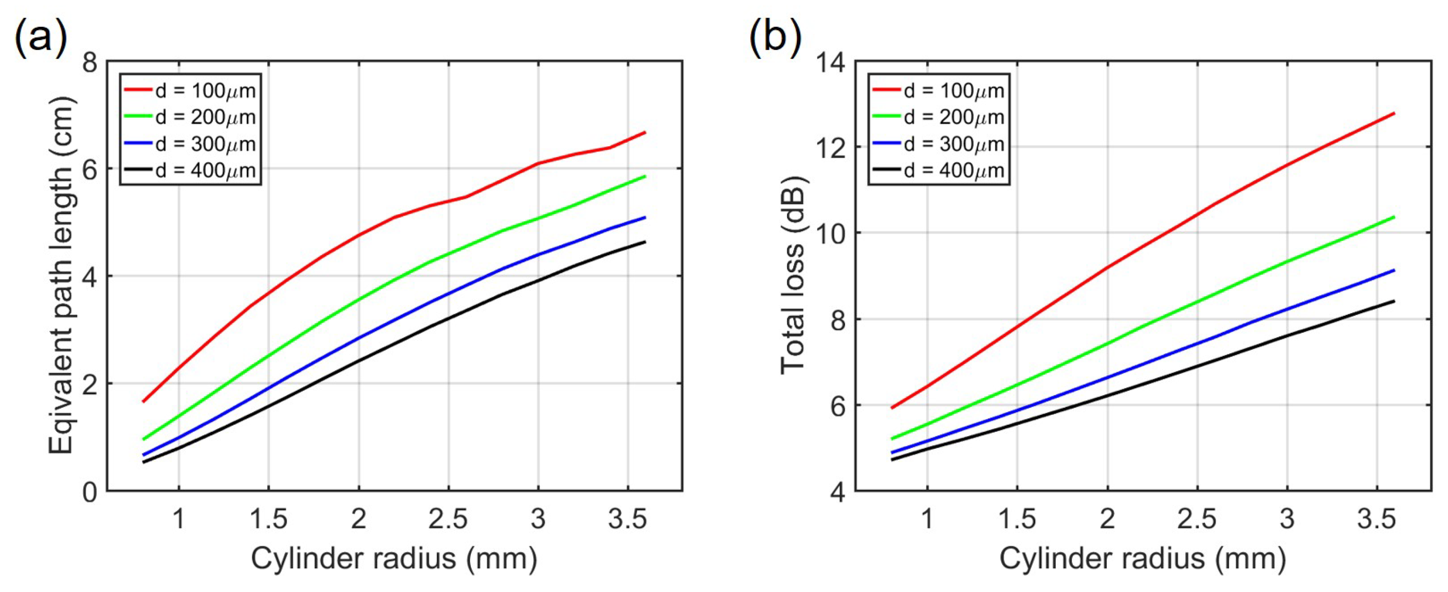
Figure 3 shows the equivalent path length as well as the total loss from the input waveguide to the output waveguide for various cavity radii R and access waveguide widths d. In this simulation we used α C O 2 = 0.03/cm, which is equivalent to the absorption of 1000 ppm CO2 averaged over 4.2–4.35 µm.
One can see that as the cavity radius increases or the access waveguide width decreases, the equivalent path length increases. This is because light is trapped inside the cavity for a longer time and has a lower probability to escape to the access waveguides, resulting in a longer equivalent path length. Consequently, light experience more reflections on average and thus the total loss increases.
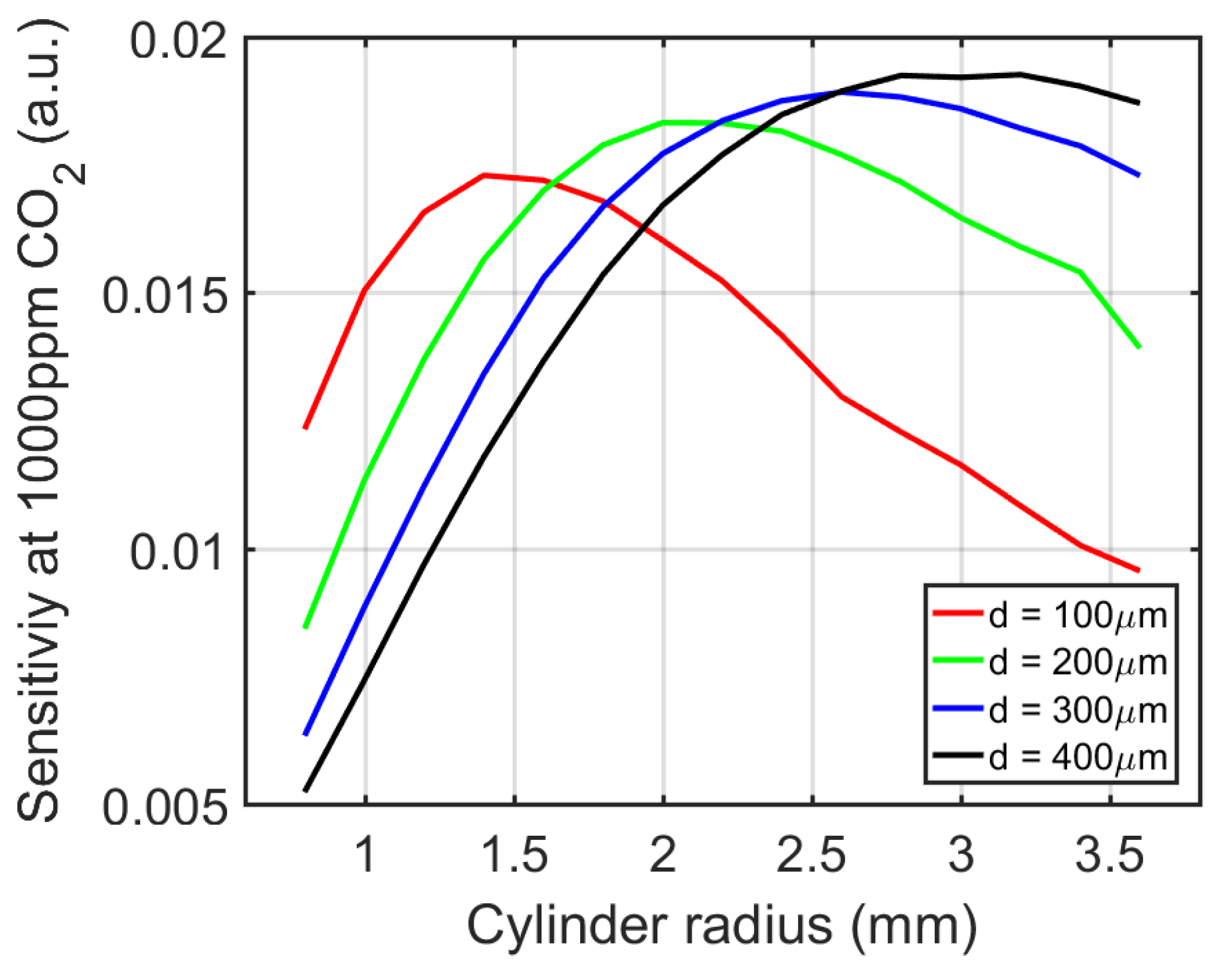
To optimize the design, namely to maximize the sensitivity S (i.e., transmission change for a CO2 concentration change of 1000 ppm) induced by the CO2 absorption, the sensitivity S for various cylinder radii and access waveguide widths is plotted in Figure 4.
We can see that as we increase the cylinder radius R with fixed access waveguide width d, the sensitivity S first increases and then decreases. The optimal radius R is defined as the radius when S is at its maximum. Table 1 summarizes the optimal radius for different access waveguide widths. We can also see that at optimal cylinder radius, both the total loss and the equivalent path length extracted from the simulations are nearly constant, which agrees with theory. As a tradeoff between maximum response and device footprint, we choose a sensor with cylinder radius R = 2 mm and access waveguide width d = 200 µm. Such a sensor gives an equivalent path length of 3.5 cm, which is considerable given the small footprint of the sensor.

5. Sensor Fabrication and Experimental Setup

5.1. Sensor Fabrication

Figure 5a shows the fabrication process of the sensor. To make the sensor on-chip, we started with two blank Si substrates. On the bottom substrate, a cylindrical cavity with one input waveguide and two output waveguides was etched by Deep Reactive Ion Etching (DRIE), as shown in Figure 5b. On the circular boundary of the cavity, a roughness function was deliberately applied, such that the incident light is scattered randomly. After etching, a thin layer of titanium and gold(Ti/Au∼30 nm/500 nm) was sputtered on the bottom substrate as well as on the (planar) top substrate. The reason we used gold as reflector is that it has very high(∼99.5%) reflectivity in the 4 µm wavelength range [32]. After gold deposition, the two substrates underwent an Ar plasma treatment (pressure = 53 mTorr, power = 100 W, duration = 60 s), and were bonded using gold-to-gold direct bonding (at 300 °C, 1 MPa for 30 min). Figure 5c shows a Si chip after bonding, the chip consists of 2 sensors.

5.2. Measurement Setup

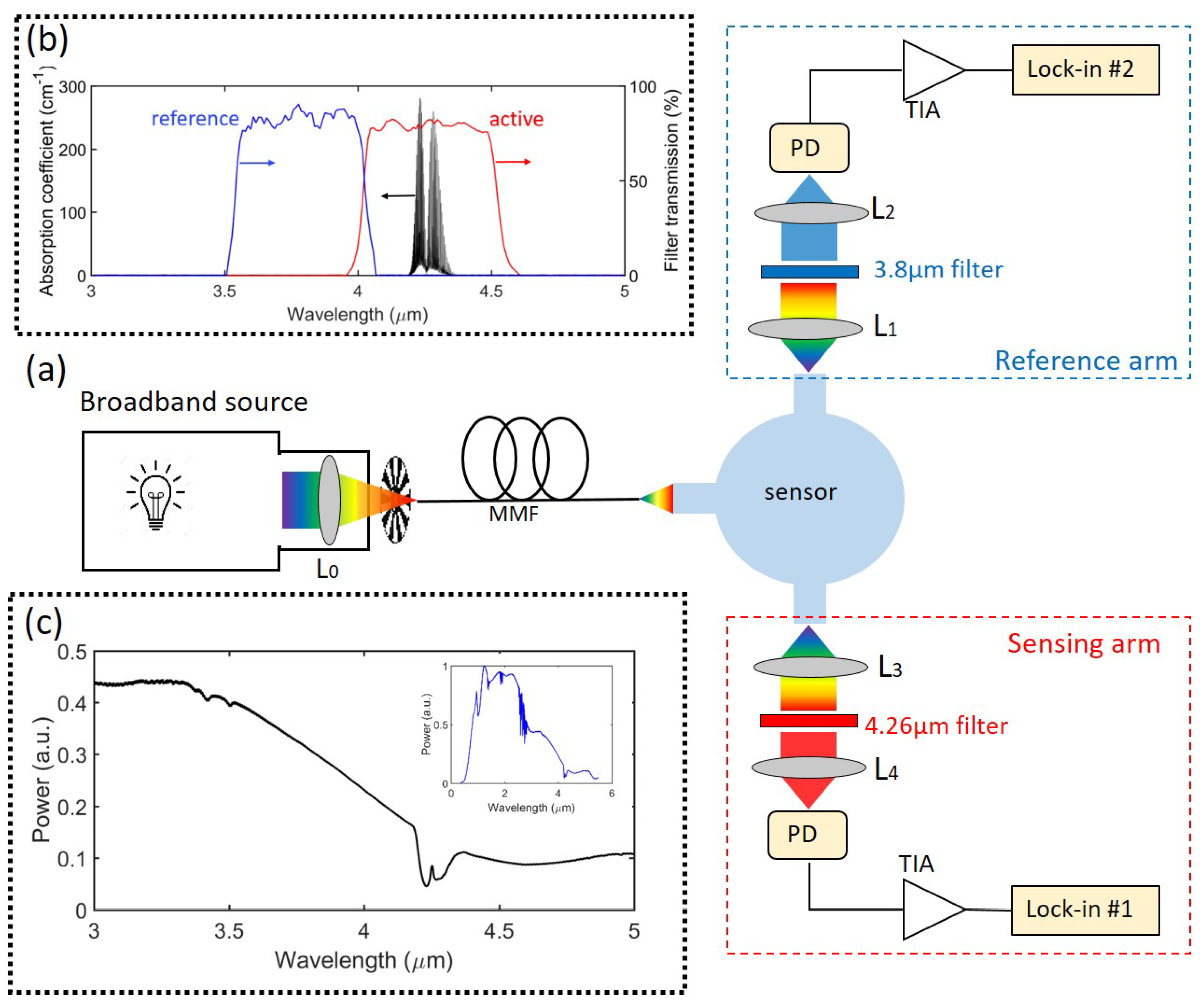
To experimentally evaluate the fabricated sensor, we built the setup as shown in Figure 6. The light emitted from a stabilized broadband source (SLS202, with SLS202C collimation package, Thorlabs, Newton, NJ, USA) is passed through a lens(LA5315-E, Thorlabs, Newton, NJ, USA) and focused onto a multimode fiber (CIR500/550, Artphotonics, Berlin, Germany). An optical chopper (MC1F10 blade with MC2000 controller, Thorlabs, Newton, NJ, USA) is placed between the lens and fiber to modulate the continuous wave light. Then light is butt-coupled from the fiber to the input waveguide of the sensor (fiber to input waveguide distance ∼50 µm). At the output waveguide of the sensing arm, light is collimated and re-focused onto a photodiode by two identical lenses (C037TME-E, Thorlabs, Newton, NJ, USA), with a band pass filter (FB4250-500, Thorlabs, Newton, NJ, USA) in between. The lens-filter-lens system is sealed and isolated from the ambient to avoid excess absorption loss by a CO2 concentration change in the gap between lenses and filter. We use a commercial un-cooled photodiode (P13023-013CA, Hamamatsu, Japan) as a detector. A customized trans-impedance amplifier (TIA) is designed and fabricated in-house to amplify the signal. A lock-in amplifier (SR830, Stanford Research Systems, Sunnyvale, CA, USA) is used for data acquisition and readout. The reference arm only differs in the optical filter, with pass band centered at λ 0 = 3.75 µm (FB3750-500, Thorlabs, Newton, NJ, USA), the two arms are otherwise identical. The transmission spectra of the active and reference filters are shown in Figure 6b. CO2 gas was supplied from certified cylinders (PRAXAIR Gases, Danbury, CT, USA). Sample gas with various concentrations of CO2 is generated by mixing CO2 and N2 through two mass flow controllers (M13212646C, Bronkhorst, Netherlands), and the sample gas is fed into the sensor by bringing the gas tube in close proximity to the sensor (not shown in the setup). During the measurement, the optical chopper works at 635 Hz, and the signals at both arms are simultaneously acquired by two lock-in amplifiers with identical settings.

6. Experimental Results

As mentioned before, the reference channel is used to compensate for source fluctuations. The source power fluctuations can be eliminated by constantly measuring the reference channel intensity I R with a correction factor I R 0 I A 0 , which can be obtained by flushing the sensor with CO2-free air at the beginning of the measurement. The normalized signal can thus be expressed as:
S n o r m = 1 I R 0 I A 0 I A I R
In all following measurement results, we use the quantity S n o r m as a figure of merit to evaluate the sensor performance.

6.1. Allan Deviation Plot

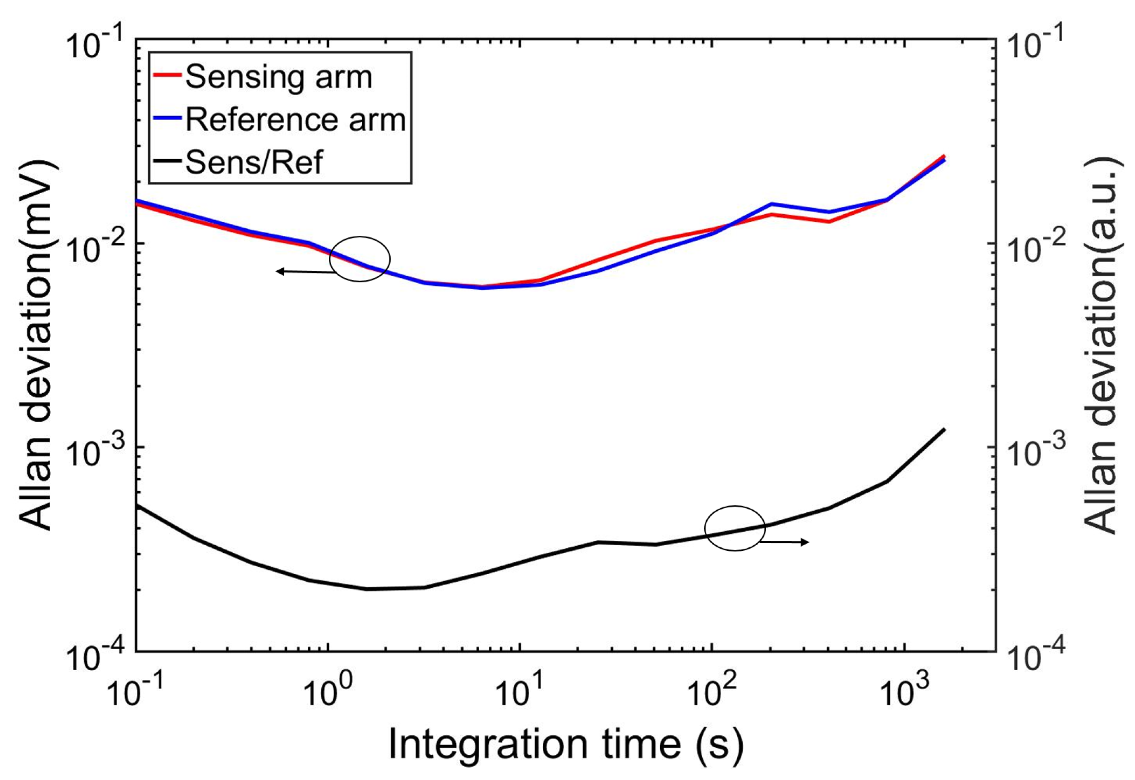
As the limit of detection (LOD) of the sensor is limited by the system noise, an Allan deviation analysis was carried out to study both system stability and theoretical LOD of the sensor. During the measurement, we flush the sensor with pure nitrogen and record the sensing signal and reference signal. The Allan deviation of both sensing signal I A and reference signal I R , as well as the normalized signal I A I R , are presented in Figure 7. One can see that the optimal averaging time (when the Allan deviation of the normalized signal is at its minimum), is approximately 2 s, and the minimum transmission change that can be measured is 0.0002 (1 σ ). In all following measurements an integration time of 1 second was used, which is restricted by the limited resolution of the lock-in time constant in the experiment.

6.2. CO2 Response

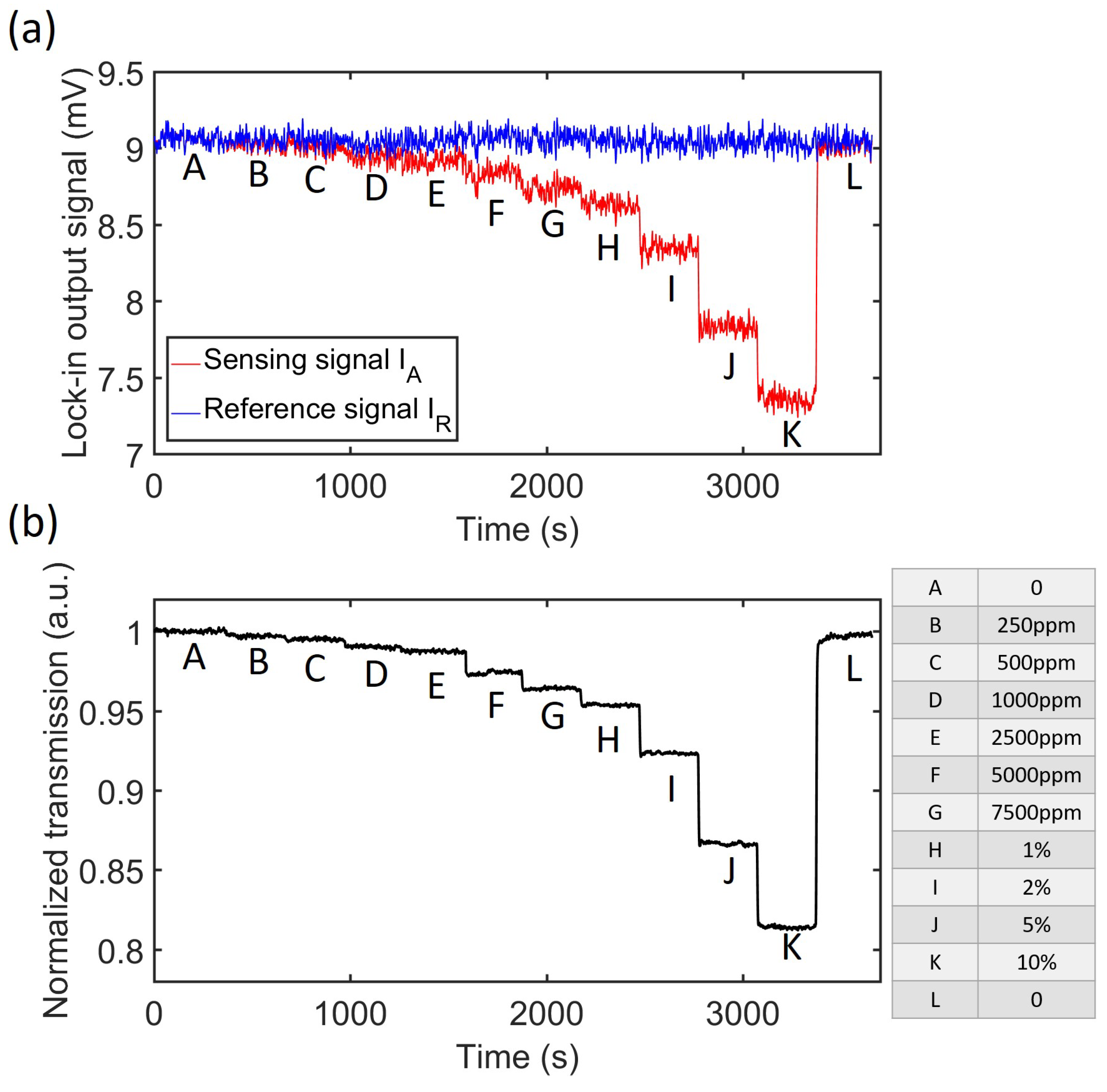
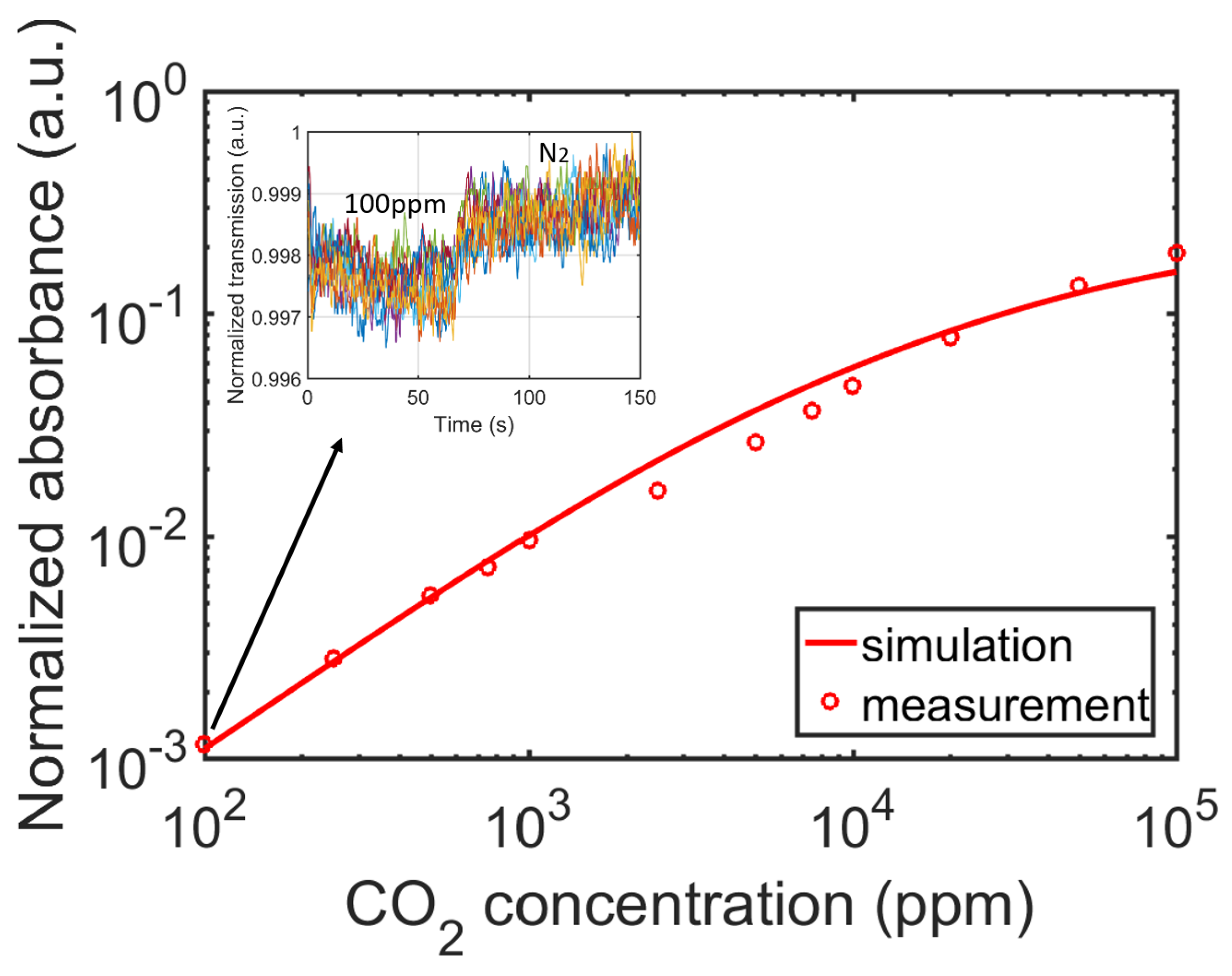
To measure the response of the sensor to CO2 concentration change, a series of sample gases with different CO2 concentrations were generated and fed into the sensor. At each concentration step, the sensing signal I A and the reference signal I R were recorded for a period of 5 min, as shown in Figure 8a. It can be seen that the reference signal stays relatively stable while the sensing signal responds to CO2 concentration changes. Moreover, a strong correlation can be observed between the two signals, due to the common mode noise on both arms. These fluctuations can be eliminated by calculating the normalized signal I A I R , shown in Figure 8b, with the CO2 concentration sequence listed on the right side. According to Equation (6), we can calculate the normalized signal S n o r m for each CO2 concentration. The values of I R 0 and I A 0 are obtained by flushing the sensor with pure nitrogen at the beginning of the measurement. The calculated normalized absorbance is plotted in Figure 9. We also simulated the absorbance by propagating the source spectrum (shown in Figure 6c) through the active filter (shown in Figure 6b) and then through CO2, using an equivalent path length of 3.5 cm (as obtained from Figure 3a). One can see that the simulation and the measurement agree reasonably well. The inset in Figure 9 shows the normalized signal I A I R of 100 ppm CO2, where we flushed the sensor first with 100 ppm CO2 and then with pure nitrogen, the inset shows 10 such measurements superimposed over one figure. A clear and repeatable step response is observed at 100 ppm CO2.

6.3. Response Time

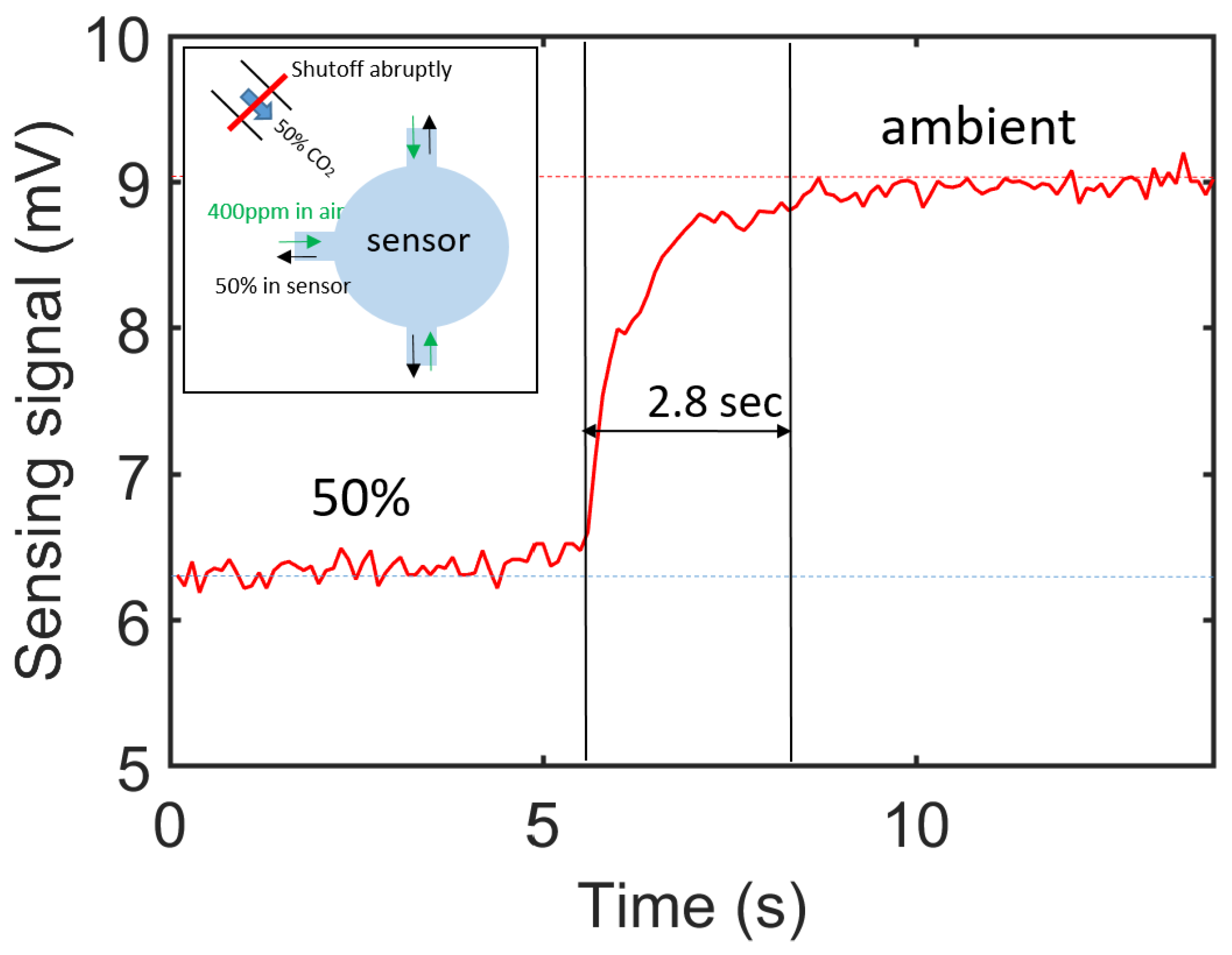
Response time is an important characteristic of the sensor, as fast response time enables real time detection, which is of great importance for applications such as in MAC leak detection. Response time is defined as the time needed for the sensor to reach 90% of the total response when there is a step concentration change. To measure the response time of the sensor, we used the same experimental setup as shown in Figure 6a, the measurement method is shown in the inset of Figure 10. We first flushed the sensor with a sample gas containing 50% of CO2, and recorded the sensing signal when the reading became stable. Then we abruptly shut off the gas flow such that the CO2 concentration reaches ambient level (∼400 ppm). The measured time trace sensing signal is shown in Figure 10. It can be seen that the response time (from 10% to 90%) of the sensor is approximately 2.8 s, due to the sensor’s small footprint.

7. Conclusions and Outlook

In summary, a miniaturized CO2 sensor based on the NDIR working principle is demonstrated in this work. The sensor has a gold-coated cylindrical cavity with one input waveguide and two output waveguides, in which light experiences multiple reflections and as such the optical path length is effectively increased. The design of the sensor is optimized by simulations with 3D ray tracing. We show that with an access waveguide width of 200 µm and a cylinder radius of 2 mm, the sensor can have an equivalent path length of 3.5 cm on a footprint of only 6 mm × 6 mm. The sensor was fabricated using DRIE and wafer bonding on silicon. To characterize the sensor, CO2 sensing measurements were performed, showing a limit of detection of 100 ppm. The sensor response time was also measured to be 2.8 s. The use of DRIE-based waveguide structures enables mass fabrication, as well as the co-integration of flip-chip integrated mid-IR LEDs and photodetectors to achieve a fully integrated sensing system. Specific performance of the sensor such as long-term stability and cross-sensitivity will be investigated when a fully integrated CO2 sensor is available in our future work.

Author Contributions

Data curation, X.J.; Formal analysis, X.J.; Funding acquisition, R.B. and G.R.; Investigation, X.J.; Methodology, X.J.; Project administration, G.R.; Resources, J.R.; Supervision, J.R., R.B. and G.R.; Writing—original draft, X.J.; Writing—review & editing, J.R., R.B. and G.R.

Funding

This research was funded by the Flanders Innovation and Entrepreneurship Agency (VLAIO) Grant Number 160580.

Acknowledgments

The authors acknowledge Jasper Jans for implementation of the TIA, Steven Verstuyft/ Muhammad Muneeb for facilitating gold deposition, and Anton Vasiliev for useful discussions.

Conflicts of Interest

The authors declare no conflict of interest. The funders had no role in the design of the study; in the collection, analysis, or interpretation of data; in the writing of the manuscript, or in the decision to publish the results.

References

  1. Ortiz Perez, A.; Bierer, B.; Scholz, L.; Wöllenstein, J.; Palzer, S. A Wireless Gas Sensor Network to Monitor Indoor Environmental Quality in Schools. Sensors 2018, 18, 4345. [Google Scholar] [CrossRef] [PubMed]
  2. Wang, J.; Zheng, L.; Niu, X.; Zheng, C.; Wang, Y.; Tittel, F.K. Mid-infrared absorption-spectroscopy-based carbon dioxide sensor network in greenhouse agriculture: Development and deployment. Appl. Opt. 2016, 55, 7029–7036. [Google Scholar] [CrossRef] [PubMed]
  3. Wells, S.L.; DeSimone, J. CO2 technology platform: An important tool for environmental problem solving. Angew. Chem. Int. Ed. 2001, 40, 518–527. [Google Scholar] [CrossRef]
  4. Europe Advanced CO2 Sensor Market Analysis—Global Forecast 2016 to 2022. Available online: https://www.marketresearchfuture.com/reports/europe-advanced-co2-sensor-market-2574 (accessed on 30 May 2019).
  5. Directive 2006/40/EC of the European Parliament and of the Council of 17 May 2006 Relating to Emissions from air-Conditioning Systems in Motor Vehicles and Amending Council Directive 70/156/EEC. Available online: https://eur-lex.europa.eu/LexUriServ/LexUriServ.do?uri=OJ:L:2006:161:0012:0018:EN:PDF (accessed on 28 May 2019).
  6. Aprea, C.; Greco, A.; Maiorino, A. The substitution of R134a with R744: An exergetic analysis based on experimental data. Int. J. Refrig. 2013, 36, 2148–2159. [Google Scholar] [CrossRef]
  7. Malvicino, C.; Seccardini, R.; Markowitz, M.; Schuermanns, K.; Bergami, A.; Arnaud, C.; Haller, R.; Petitjean, C.; Strupp, C.; Lemke, N.; et al. B-Cool pRoject-Ford Ka and Fiat Panda r-744 Mac Systems; 2009-01-0967; SAE International: Warrendale, PA, USA, 2009. [Google Scholar]
  8. Law, J.; Watkins, S.; Alexander, D. In-flight carbon dioxide exposures and related symptoms: Association, susceptibility, and operational implications. NASA Tech. Pap. 2010, 2010, 216126. [Google Scholar]
  9. Satish, U.; Mendell, M.J.; Shekhar, K.; Hotchi, T.; Sullivan, D.; Streufert, S.; Fisk, W.J. Is CO2 an indoor pollutant? Direct effects of low-to-moderate CO2 concentrations on human decision-making performance. Environ. Health Perspect. 2012, 120, 1671–1677. [Google Scholar] [CrossRef]
  10. Allen, J.G.; MacNaughton, P.; Satish, U.; Santanam, S.; Vallarino, J.; Spengler, J.D. Associations of cognitive function scores with carbon dioxide, ventilation, and volatile organic compound exposures in office workers: A controlled exposure study of green and conventional office environments. Environ. Health Perspect. 2015, 124, 805–812. [Google Scholar] [CrossRef] [PubMed]
  11. Willa, C.; Yuan, J.; Niederberger, M.; Koziej, D. When Nanoparticles Meet Poly(Ionic Liquid)s: Chemoresistive CO2 Sensing at Room Temperature. Adv. Funct. Mater. 2015, 25, 2537–2542. [Google Scholar]
  12. Kreno, L.E.; Leong, K.; Farha, O.K.; Allendorf, M.; Van Duyne, R.P.; Hupp, J.T. Metal—organic framework materials as chemical sensors. Chem. Rev. 2011, 112, 1105–1125. [Google Scholar] [CrossRef]
  13. Puligundla, P.; Jung, J.; Ko, S. Carbon dioxide sensors for intelligent food packaging applications. Food Control 2012, 25, 328–333. [Google Scholar] [CrossRef]
  14. Boudaden, J.; Klumpp, A.; Eisele, I.; Kutter, C. Smart capacitive CO2 sensor. In Proceedings of the 2016 IEEE SENSORS, Orlando, FL, USA, 30 October–3 November 2016; pp. 1–3. [Google Scholar]
  15. Hodgkinson, J.; Tatam, R.P. Optical gas sensing: A review. Meas. Sci. Technol. 2012, 24, 012004. [Google Scholar] [CrossRef]
  16. Liu, X.; Cheng, S.; Liu, H.; Hu, S.; Zhang, D.; Ning, H. A survey on gas sensing technology. Sensors 2012, 12, 9635–9665. [Google Scholar] [CrossRef] [PubMed]
  17. Neethirajan, S.; Jayas, D.; Sadistap, S. Carbon dioxide (CO2) sensors for the agri-food industry—A review. Food Bioprocess Technol. 2009, 2, 115–121. [Google Scholar] [CrossRef]
  18. Massie, C.; Stewart, G.; McGregor, G.; Gilchrist, J.R. Design of a portable optical sensor for methane gas detection. Sens. Actuators Chem. 2006, 113, 830–836. [Google Scholar] [CrossRef]
  19. Thurmond, K.; Loparo, Z.; Partridge, W.; Vasu, S.S. A light-emitting diode-(LED-) based absorption sensor for simultaneous detection of carbon monoxide and carbon dioxide. Appl. Spectrosc. 2016, 70, 962–971. [Google Scholar] [CrossRef] [PubMed]
  20. Tan, Q.; Tang, L.; Yang, M.; Xue, C.; Zhang, W.; Liu, J.; Xiong, J. Three-gas detection system with IR optical sensor based on NDIR technology. Opt. Lasers Eng. 2015, 74, 103–108. [Google Scholar] [CrossRef]
  21. Tan, Q.; Pei, X.; Zhu, S.; Sun, D.; Liu, J.; Xue, C.; Liang, T.; Zhang, W.; Xiong, J. Development of an optical gas leak sensor for detecting ethylene, dimethyl ether and methane. Sensors 2013, 13, 4157–4169. [Google Scholar] [CrossRef]
  22. Gibson, D.; MacGregor, C. A novel solid state non-dispersive infrared CO2 gas sensor compatible with wireless and portable deployment. Sensors 2013, 13, 7079–7103. [Google Scholar] [CrossRef]
  23. Hodgkinson, J.; Smith, R.; Ho, W.O.; Saffell, J.R.; Tatam, R.P. Non-dispersive infra-red (NDIR) measurement of carbon dioxide at 4.2 μm in a compact and optically efficient sensor. Sens. Actuators Chem. 2013, 186, 580–588. [Google Scholar] [CrossRef]
  24. Ayerden, N.P.; de Graaf, G.; Wolffenbuttel, R.F. Compact gas cell integrated with a linear variable optical filter. Opt. Express 2016, 24, 2981–3002. [Google Scholar] [CrossRef]
  25. Ayerden, N.P.; Ghaderi, M.; Enoksson, P.; de Graaf, G.; Wolffenbuttel, R.F. A miniaturized optical gas-composition sensor with integrated sample chamber. Sens. Actuators Chem. 2016, 236, 917–925. [Google Scholar] [CrossRef]
  26. Moumen, S.; Raible, I.; Krauß, A.; Wöllenstein, J. Infrared investigation of CO2 sorption by amine based materials for the development of a NDIR CO2 sensor. Sens. Actuators Chem. 2016, 236, 1083–1090. [Google Scholar] [CrossRef]
  27. Sklorz, A.; Schafer, A.; Lang, W. Merging ethylene NDIR gas sensors with preconcentrator-devices for sensitivity enhancement. Sens. Actuators Chem. 2012, 170, 21–27. [Google Scholar] [CrossRef]
  28. Jia, X.; Roelkens, G.; Baets, R.; Roels, J. A miniaturized non-dispersive infrared CO2 sensor based on a 2D integrating cylinder. In Proceedings of the Optical Sensors and Sensing Congress, San Jose, CA, USA, 25–27 June 2019. [Google Scholar]
  29. Rothman, L.S.; Gordon, I.E.; Babikov, Y.; Barbe, A.; Benner, D.C.; Bernath, P.F.; Birk, M.; Bizzocchi, L.; Boudon, V.; Brown, L.R.; et al. The HITRAN2012 molecular spectroscopic database. J. Quant. Spectrosc. Radiat. Transf. 2013, 130, 4–50. [Google Scholar] [CrossRef]
  30. Circle Line Picking. Available online: http://mathworld.wolfram.com/CircleLinePicking.html (accessed on 30 May 2019).
  31. Fohrmann, L.S.; Sommer, G.; Pitruzzello, G.; Krauss, T.F.; Petrov, A.Y.; Eich, M. Integrating cell on chip—Novel waveguide platform employing ultra-long optical paths. APL Photonics 2017, 2, 096102. [Google Scholar] [CrossRef]
  32. Babar, S.; Weaver, J. Optical constants of Cu, Ag, and Au revisited. Appl. Opt. 2015, 54, 477–481. [Google Scholar] [CrossRef]
  33. Tholabs Inc. Available online: https://www.thorlabs.com/ (accessed on 30 May 2019).
Figure 1. Schematic of a typical NDIR sensor. The sensor consists of an infrared broadband source, a reflecting gas tube with gas inlet and outlet, a pair of optical filters(active and reference), and two optical detectors. The two filters and two detectors form the active channel and reference channel, respectively.
Sensors 19 04260 g001
Figure 2. (a) 3D schematic of the proposed sensor structure. The bottom substrate has a gold-coated hollow cylindrical cavity with one input waveguide and two output waveguides, the upper substrate is a gold-coated planar silicon substrate, the sensor is formed by wafer bonding of both substrates. (b) 2D schematic of the sensor, where R is the radius of the circle, d is the width of all access waveguides, P is the power coupled into the cavity, P W G , P r a d and P p r o p are the power coupled to the output waveguides, the power absorbed/radiated at the cavity sidewall, and the power lost during propagation in the cavity, respectively.
Sensors 19 04260 g002
Figure 3. Simulation of the integrating cylinder with various cylinder radius and waveguide width combinations, the height of the cylinder is kept at 300 µm. (a) Equivalent path length. (b) Total transmission loss.
Sensors 19 04260 g003
Figure 4. Sensor sensitivity S at CO2 = 1000 ppm, for various cylinder radius and access waveguide width combinations.
Sensors 19 04260 g004
Figure 5. (a) Fabrication process of the sensor. Before wafer bonding, the two substrates undergo Ar plasma treatment. (b) Two cylindrical cavities etched on the bottom substrate with DRIE, the etching depth is 300 µm, the length of the access waveguides is 1mm. (c) Fabricated chip with a EURO 10 cent coin, the chip contains two sensors.
Sensors 19 04260 g005
Figure 6. (a) Experimental setup. L: lens MMF: multimode fiber, PD: photodiode, TIA: trans-impedance amplifier. (b) Transmission spectrum of the optical filters used in this work(reproduced from [33]), superimposed on the CO2 absorption spectrum in 3–5 µm wavelength range [29]. (c) Source spectrum in 3–5 µm wavelength range, a full spectrum is also in the inset, also reproduced from [33].
Sensors 19 04260 g006
Figure 7. Allan deviation plot of the sensing and reference arm, as well as the normalized signal (in pure N2 environment).
Sensors 19 04260 g007
Figure 8. (a) Response of both sensing signal and reference signal to CO2 concentration steps, the sensing and reference signal exhibit a strong correlation. (b) Normalized transmission, obtained by dividing the sensing signal with the reference signal. The CO2 concentration steps are listed on the right side.
Sensors 19 04260 g008
Figure 9. Normalized absorbance of the sensor at various CO2 concentrations. The inset shows the step response of the sensor at CO2 = 100 ppm, with 10 measurements superimposed in one figure.
Sensors 19 04260 g009
Figure 10. Response time of sensor, measured with 100 ms lock-in integration time. The inset shows the gas flow mechanisms when the 50% CO2 is abruptly shut off.
Sensors 19 04260 g010
Table 1. Optimal cylinder radius for different access waveguide widths, as well as the corresponding equivalent path length and total transmission loss. It can be seen that both the equivalent path length and total transmission loss are nearly constant at optimal radius.
d [um]R [mm]TL [dB]Leq [cm]
1001.47.53.4
2002.07.43.5
3002.67.63.8
4003.07.63.9