Effects of Chemical State of the Pd Species on H2 Sensing Characteristics of PdOx/SnO2 Based Chemiresistive Sensors

Abstract
1. Introduction
2. Materials and Methods
2.1. Preparation of PdOx/SnO2 Composites
2.2. Characterization
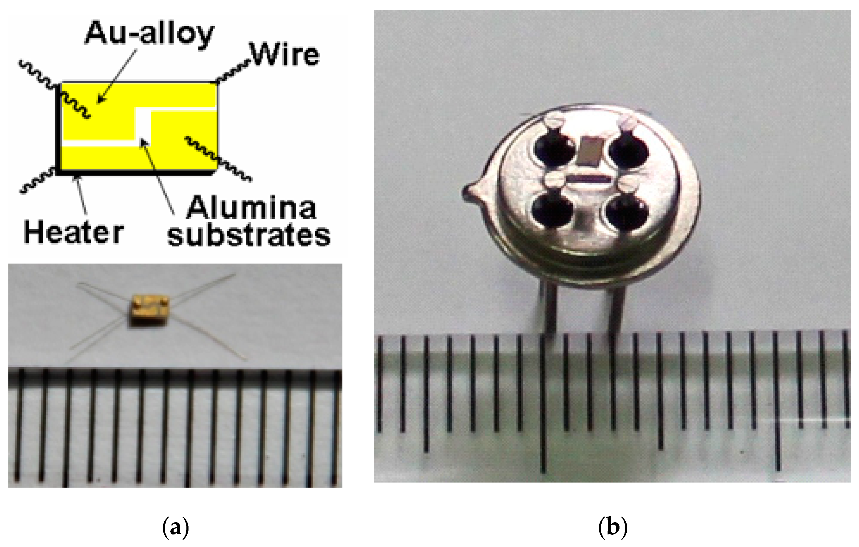
2.3. Fabrication and Measurement of Gas Sensor
3. Results and Discussion
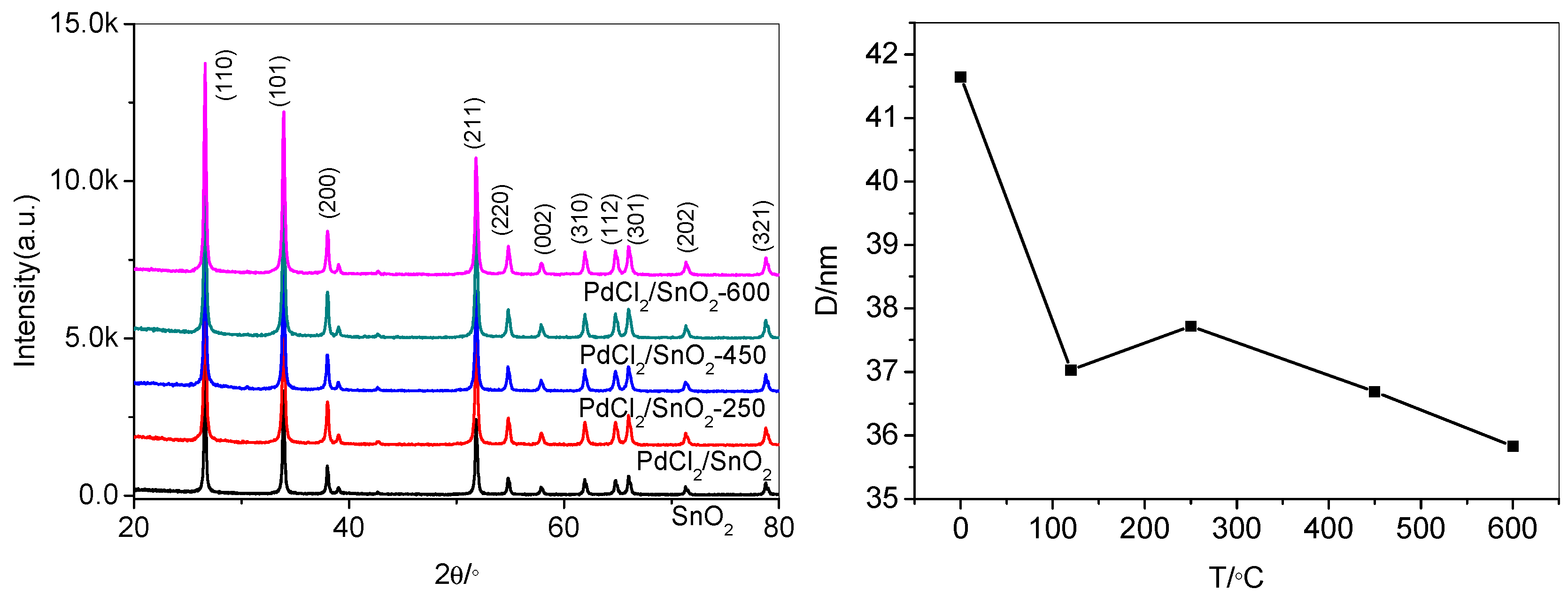
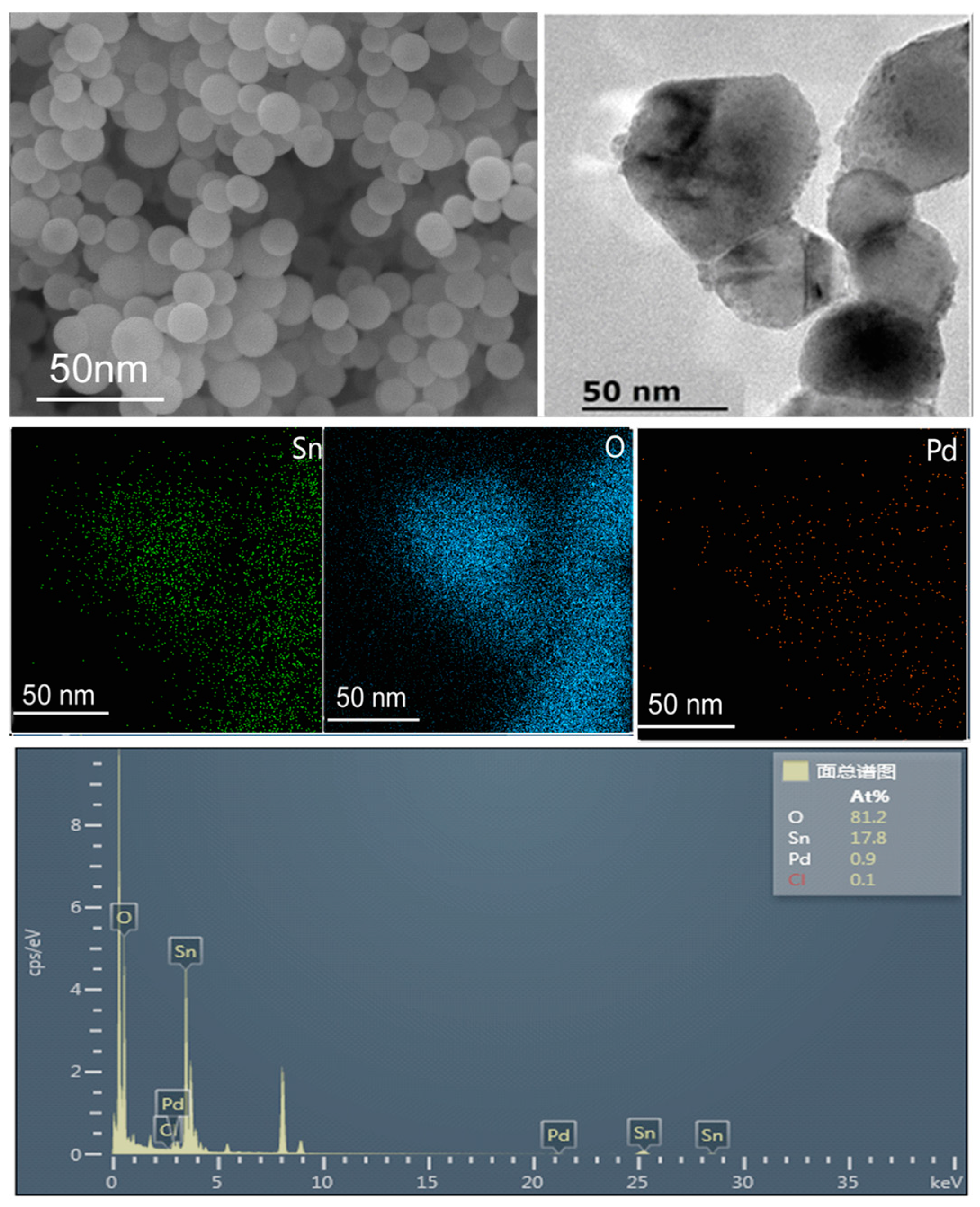
3.1. Microstructure Characterization of PdOx/SnO2 Composites
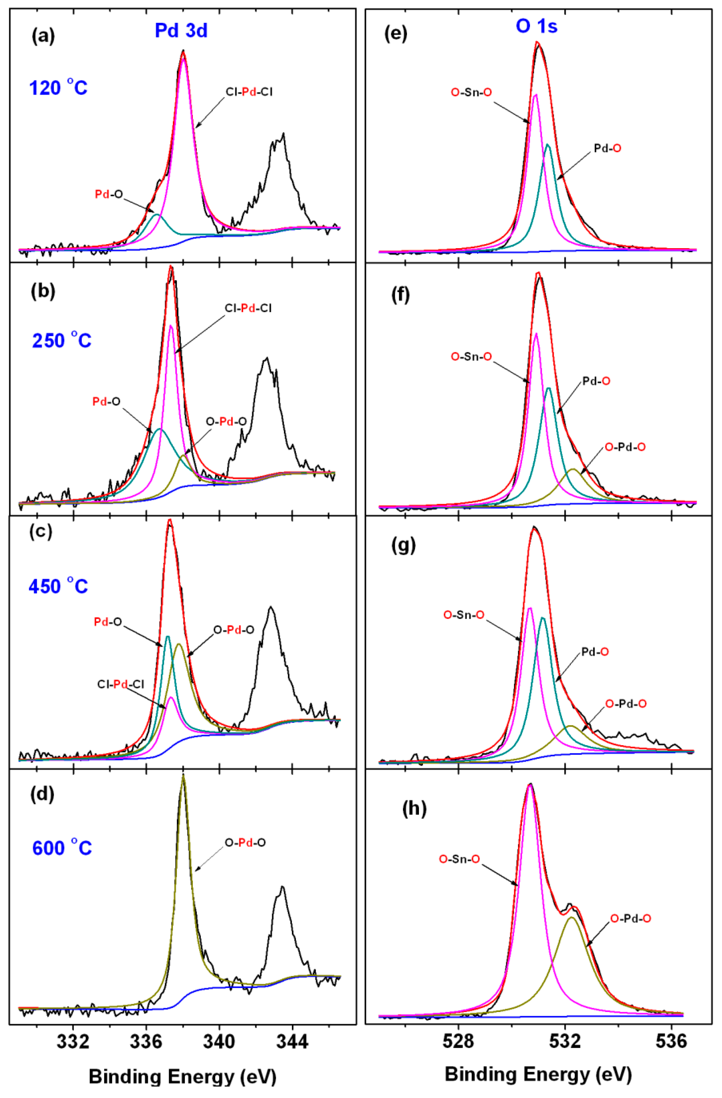
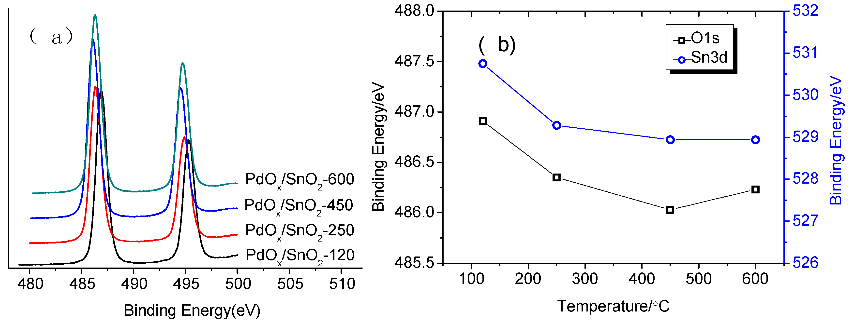
3.2. Chemical States of PdOx Dispersed on the Surfaces of SnO2
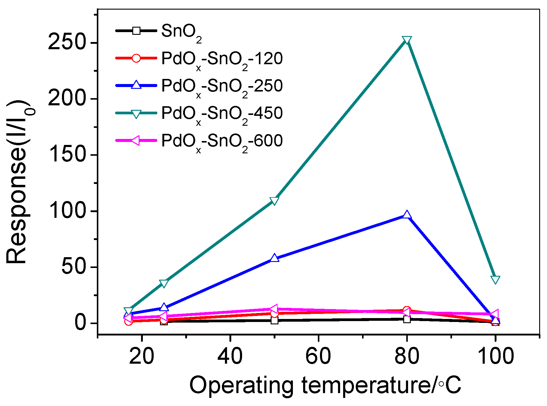
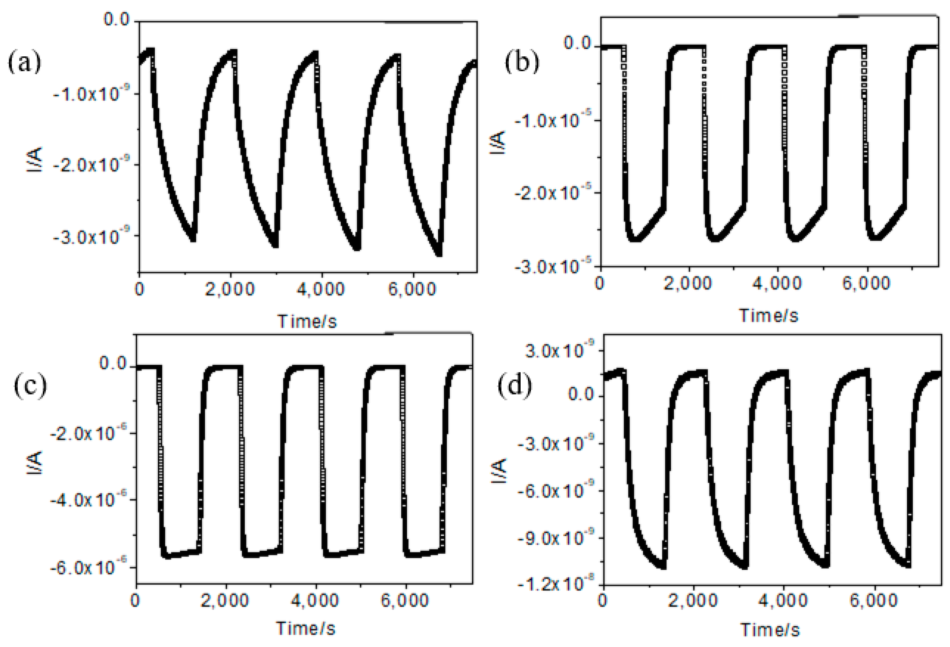
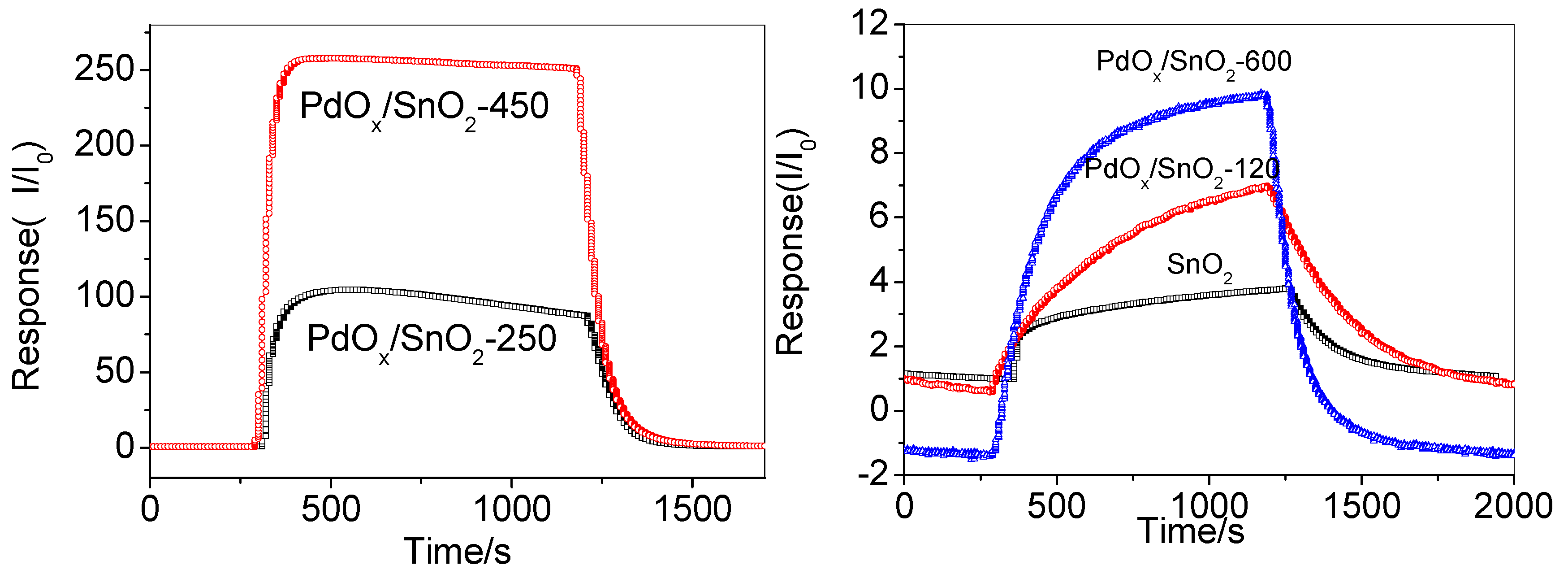
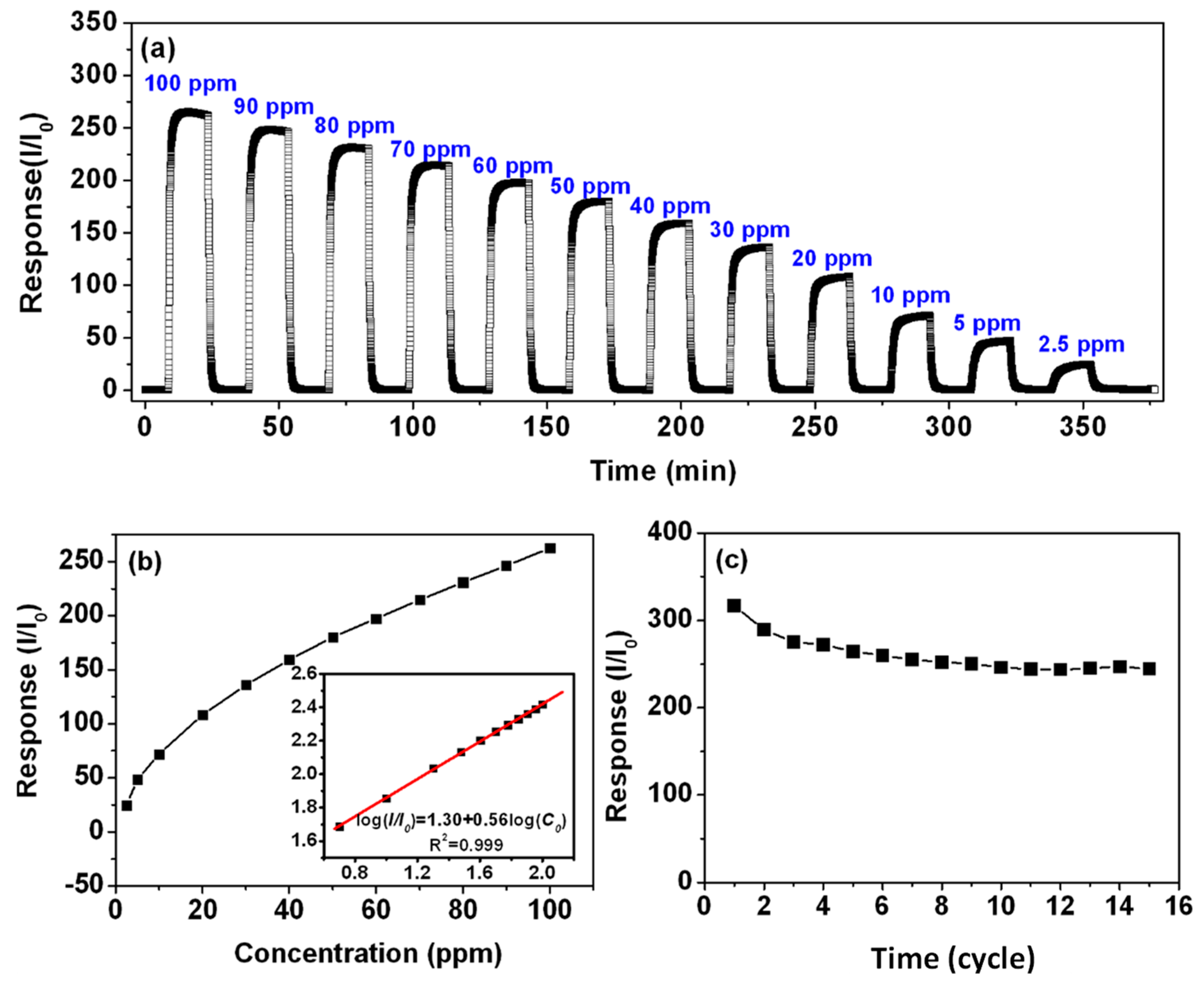
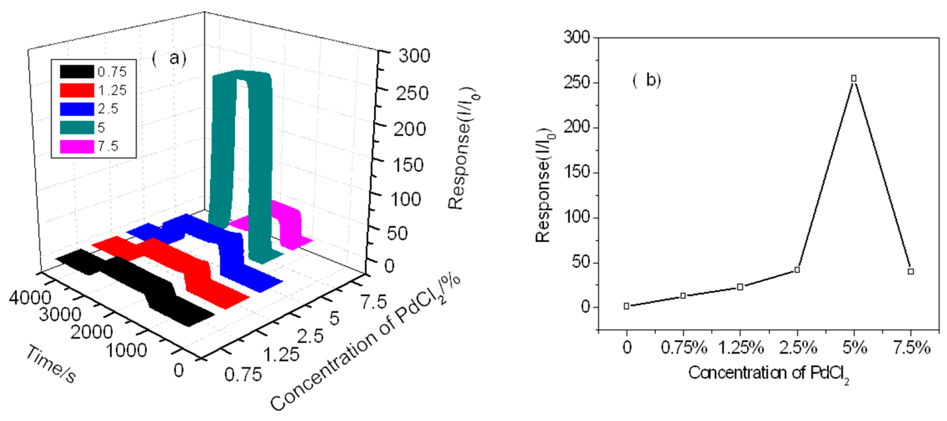
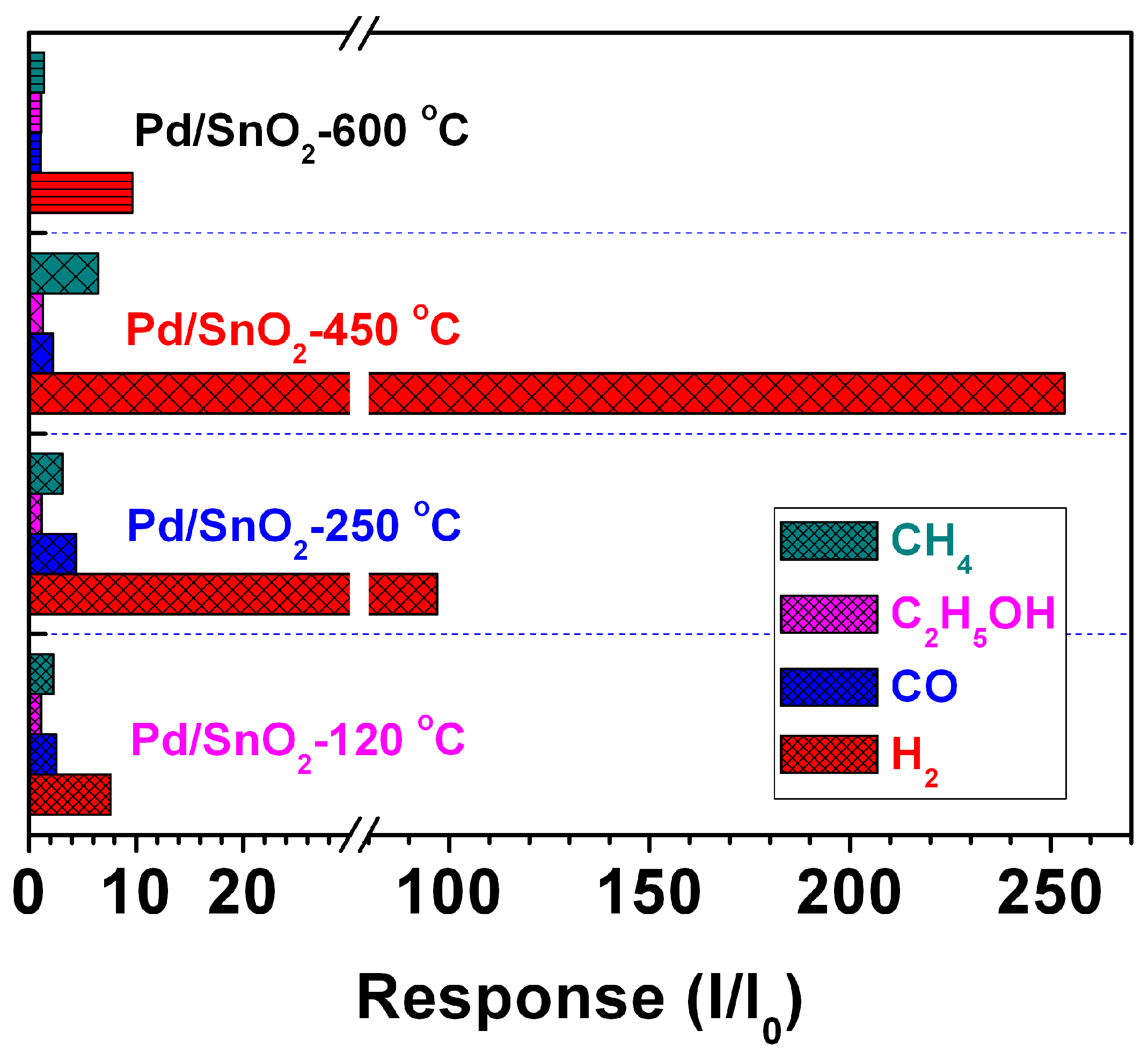
3.3. H2 Sensing Characteristics of PdOx/SnO2 Composites
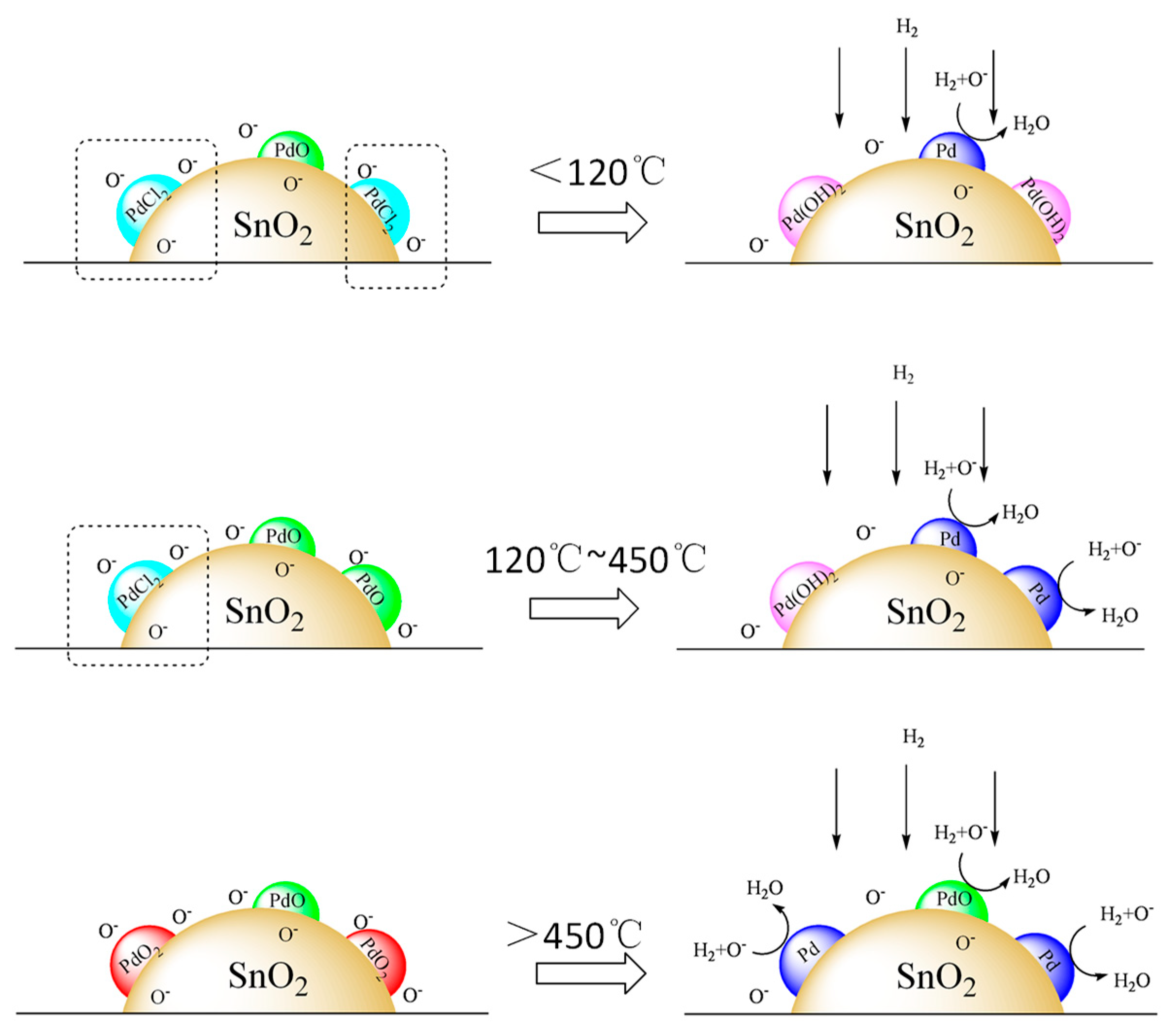
3.4. Sensing Mechanism
| Pd2+ + 2e→Pd | φ = 0.915 V. |
| Pd(OH)2 + 2e→Pd + 2OH− | φ = 0.07 V |
| [PdCl4]2− + 2e→Pd+ 4Cl− | φ = 0.621 V |
4. Conclusions
Author Contributions
Funding
Conflicts of Interest
References
- Ling, C.; Xue, Q.; Han, Z.; Lu, H.; Xia, F.; Yan, Z.; Deng, L. Room temperature hydrogen sensor with ultrahigh-responsive characteristics based on Pd/SnO2/SiO2/Si heterojunctions. Sens. Actuators B 2016, 1, 438–447. [Google Scholar] [CrossRef]
- Ayesh, A.I.; Mahmoud, S.T.; Ahmad, S.J.; Haik, Y. Novel hydrogen gas sensor based on Pd and SnO2 nanoclusters. Mater. Lett. 2014, 128, 354–357. [Google Scholar] [CrossRef]
- Wang, C.; Zeng, W.; Luo, L.; Zhang, P.; Wang, Z. Gas-sensing properties and mechanisms of Cu-doped SnO2 spheres towards H2S. Ceram. Int. 2016, 8, 10006–10013. [Google Scholar] [CrossRef]
- Su, P.; Yang, L. NH3 gas sensor based on Pd/SnO2/RGO ternary composite operated at room-temperature. Sens. Actuators B 2016, 223, 202–208. [Google Scholar] [CrossRef]
- Sa´aedi, A.; Yousefi, R.; Jamali-Sheini, F.; Zak, A.K.; Cheraghizade, M.; Mahmoudian, M.R.; Baghchesara, A.B.; Dezaki, A.S. XPS studies and photocurrent applications of alkali-metals-doped ZnO nanoparticles under visible illumination conditions. Phys. E 2016, 79, 113–118. [Google Scholar] [CrossRef]
- Lee, D.; Kim, Y.T.; Huh, J.; Lee, D. Fabrication and characteristics of SnO2 gas sensor array for volatile organic compounds recognition. Thin Solid Films 2002, 416, 271–278. [Google Scholar] [CrossRef]
- Van Duy, N.; Toan, T.H.; Hoa, N.D.; Van Hieu, N. Effects of gamma irradiation on hydrogen gas-sensing characteristics of Pd-SnO2 thin film sensors. Int. J. Hydrogen Energy 2015, 40, 12572–12580. [Google Scholar] [CrossRef]
- Lim, C.B.; Oh, S. Microstructure evolution and gas sensitivities of Pd-doped SnO2-based sensor prepared by three different catalyst-addition processes. Sens. Actuators B 1996, 30, 223–231. [Google Scholar] [CrossRef]
- Kissa, G.; Josepovits, V.K.; Kova’cs, K.; CO, Ti. Sensitivity of the PtO/SnO2 and PdO/SnO2 layer structures: Kelvin probe and XPS analysis. Thin Solid Films 2003, 436, 115–118. [Google Scholar] [CrossRef]
- Srivastava, J.K.; Pandey, P.; Mishra, V.N.; Dwivedi, R. Sensing mechanism of Pd-doped SnO2 sensor for LPG detection. Solid State Sci. 2009, 11, 1602–1605. [Google Scholar] [CrossRef]
- Li, S.; Lu, Z.; Yang, Z.; Chu, X. The sensing mechanism of Pt-doped SnO2 surface toward CO: A first-principle study. Sens. Actuators B 2014, 202, 83–92. [Google Scholar] [CrossRef]
- Liewhiran, C.; Tamaekong, N.; Wisitsoraat, A.; Tuantranont, A.; Phanichphant, S. Ultra-sensitive H2 sensors based on flame-spray-made Pd-loaded SnO2 sensing films. Sens. Actuators B 2013, 176, 893–905. [Google Scholar] [CrossRef]
- Oleksenko, L.P.; Maksymovych, N.P.; Sokovykh, E.V.; Matushko, I.P. Stability of semiconductor sensors based on nanosized SnO2 and Pd/SnO2. Russ. J. Phys. Chem. A 2014, 88, 831–835. [Google Scholar] [CrossRef]
- Liu, P.; Zhao, Y.; Qin, R.; Mo, S.; Chen, G.; Gu, L.; Chevrier, D.M.; Zhang, P.; Guo, Q.; Zang, D.; et al. Photochemical route for synthesizing atomically dispersed palladium catalysts. Science 2016, 352, 797–800. [Google Scholar] [CrossRef] [PubMed]
- Lin, Y.; Wei, W.; Li, Y.; Li, F.; Zhou, J.; Sun, D.; Chen, Y.; Ruan, S. Preparation of Pd nanoparticle-decorated hollow SnO2 nanofibers and their enhanced formaldehyde sensing properties. J. Alloys Compd. 2015, 651, 690–698. [Google Scholar] [CrossRef]
- Hu, R.-J.; Wang, J.; Zhu, H.-C. Preparation and Gas Sensing Properties of PdO, Au, CdO Coatings on SnO2 Nanofibers. Acta Phys. Chim. Sin 2015, 31, 1997–2007. [Google Scholar]
- Wang, Q.; Wang, C.; Sun, H.; Sun, P.; Wang, Y.; Lin, J.; Lu, G. Microwave assisted synthesis of hierarchical Pd/SnO2 nanostructures for CO gas sensor. Sens. Actuators B 2016, 222, 257–263. [Google Scholar] [CrossRef]
- Kim, B.; Lu, Y.; Hannon, A.; Meyyappan, M.; Li, L. Low temperature Pd/SnO2 sensor for carbon monoxide detection. Sens. Actuators B 2013, 177, 770–775. [Google Scholar] [CrossRef]
- Datye, A.K.; Bravo, J.; Nelson, T.R.; Atanasova, P.; Lyubovsky, M.; Pfefferle, L. Catalyst microstructure and methane oxidation reactivity during the Pd/PdO transformation on alumina supports. Appl. Catal. A 2000, 198, 179–196. [Google Scholar] [CrossRef]
- Yamazoe, N. New approaches for improving semiconductor gas sensors. Sens. Actuators B 1991, 5, 7–19. [Google Scholar] [CrossRef]
- Iltona, E.S.; Post, J.E.; Heaneyc, P.J.; Ling, F.T.; Kerisit, S.N. XPS determination of Mn oxidation states in Mn (hydr)oxides. Appl. Surf. Sci. 2016, 366, 475–485. [Google Scholar] [CrossRef]
- Kibis, L.S.; Titkov, A.I.; Stadnichenko, A.I.; Koscheev, S.K.; Boronin, A.I. X-ray photoelectron spectroscopy study of Pd oxidation by RF discharge in oxygen. Appl. Surf. Sci. 2009, 255, 9248–9254. [Google Scholar] [CrossRef]
- Yan, L.; Pan, J.S. XPS studies of room temperature magnetic Co-doped SnO2 deposited on Si. Mater. Sci. Eng. B 2006, 128, 34–36. [Google Scholar] [CrossRef]
- Baek, D.-H.; Kim, J. MoS2 gas sensor functionalized by Pd for the detection of hydrogen. Sens. Actuators B 2017, 250, 686–691. [Google Scholar] [CrossRef]
- Cho, S.-Y.; Ahn, H.; Park, K.; Choi, J.; Kang, H.; Jung, H.-T. Ultrasmall Grained Pd Nanopattern H2 Sensor. ACS Sens. 2018, 3, 1876–1883. [Google Scholar] [CrossRef]
- Tang, Z.; Zhang, Y.; Deng, X.; Dai, Y.; Zhang, W.; Fan, F.; Qing, B.; Zhu, C.; Fan, J.; Shi, Y. The H2 sensing properties of facets-dependent Pd nanoparticles-supported ZnO nanorods. Dalton Trans. 2018, 47, 15331–15337. [Google Scholar] [CrossRef] [PubMed]


| Compound Bulk | Pd 3d5/2 BE (eV) |
|---|---|
| Pd | 334.8–335.1 |
| PdOx,x < 1 | 335.3 |
| Pd-O | 336.9 |
| O-Pd-O | 337.9 |
| Cl-Pd-Cl | 337.8 |
© 2019 by the authors. Licensee MDPI, Basel, Switzerland. This article is an open access article distributed under the terms and conditions of the Creative Commons Attribution (CC BY) license (http://creativecommons.org/licenses/by/4.0/).
Share and Cite
Qi, T.; Sun, J.; Yang, X.; Yan, F.; Zuo, J. Effects of Chemical State of the Pd Species on H2 Sensing Characteristics of PdOx/SnO2 Based Chemiresistive Sensors. Sensors 2019, 19, 3131. https://doi.org/10.3390/s19143131
Qi T, Sun J, Yang X, Yan F, Zuo J. Effects of Chemical State of the Pd Species on H2 Sensing Characteristics of PdOx/SnO2 Based Chemiresistive Sensors. Sensors. 2019; 19(14):3131. https://doi.org/10.3390/s19143131
Chicago/Turabian StyleQi, Tianjiao, Jie Sun, Xi Yang, Fanfan Yan, and Ji Zuo. 2019. "Effects of Chemical State of the Pd Species on H2 Sensing Characteristics of PdOx/SnO2 Based Chemiresistive Sensors" Sensors 19, no. 14: 3131. https://doi.org/10.3390/s19143131
APA StyleQi, T., Sun, J., Yang, X., Yan, F., & Zuo, J. (2019). Effects of Chemical State of the Pd Species on H2 Sensing Characteristics of PdOx/SnO2 Based Chemiresistive Sensors. Sensors, 19(14), 3131. https://doi.org/10.3390/s19143131