Fabrication Technology and Characteristics Research of a Monolithically-Integrated 2D Magnetic Field Sensor Based on Silicon Magnetic Sensitive Transistors

Abstract
:1. Introduction
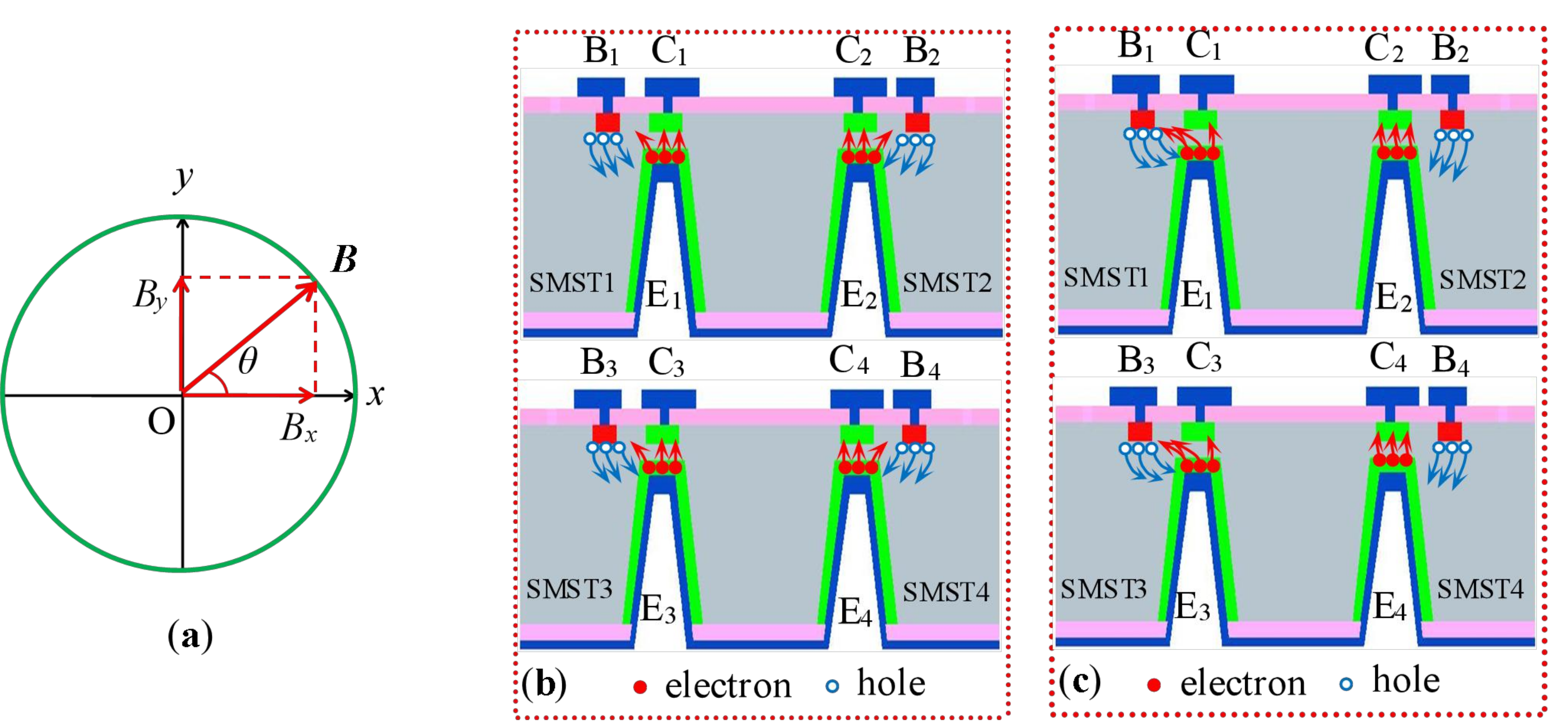
2. Basic Structure and Working Principle
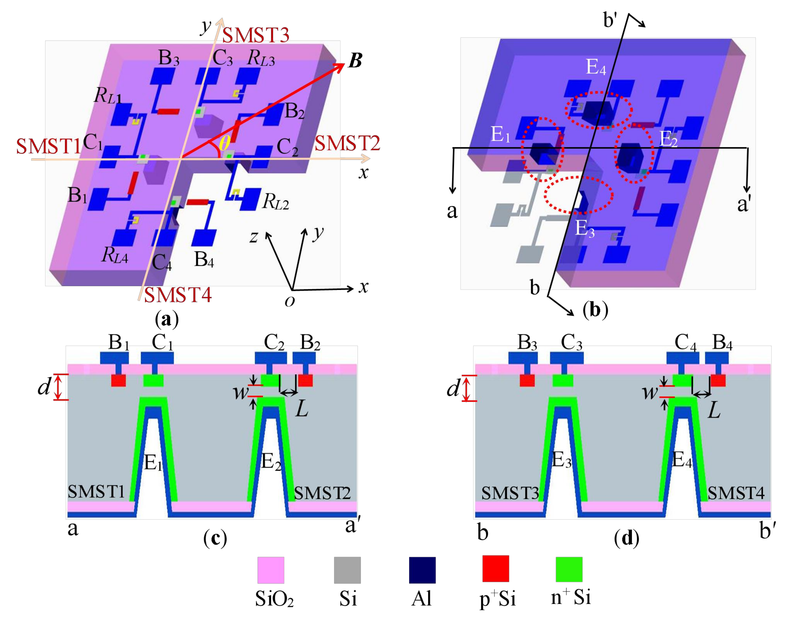
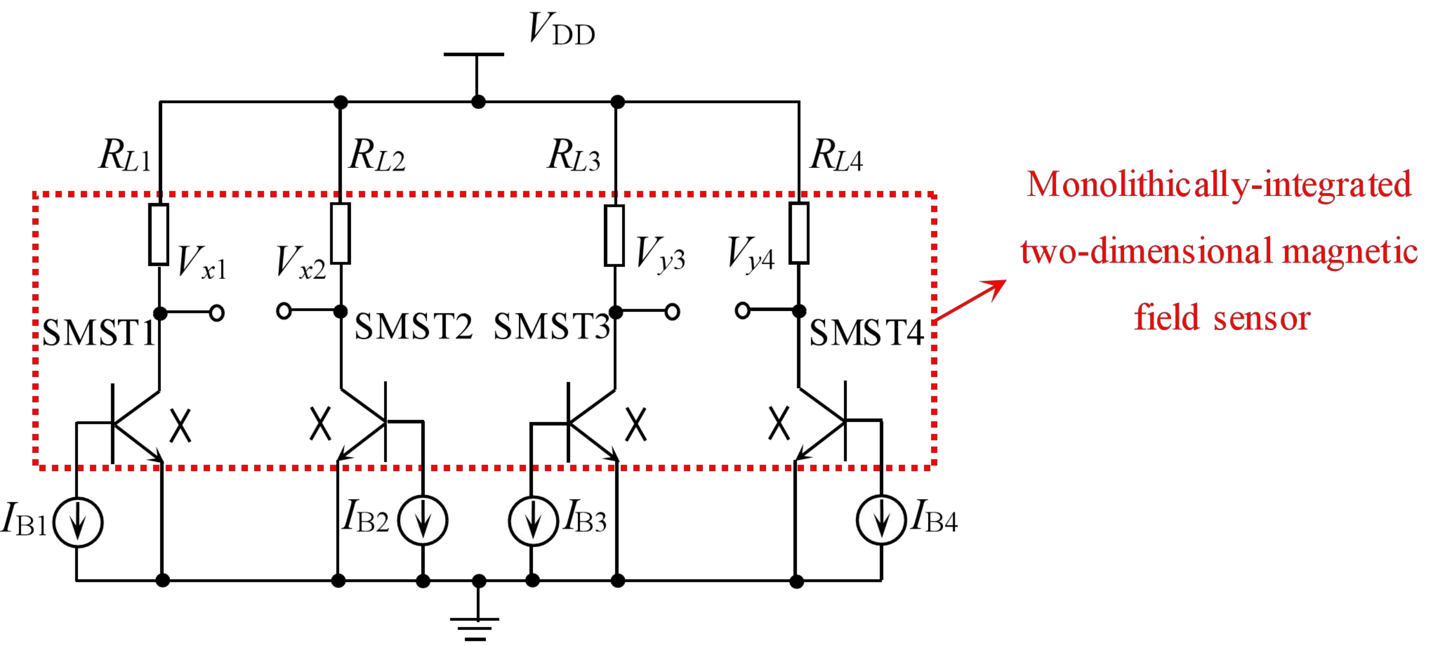
2.1. Basics Structure
2.2. Working Principle
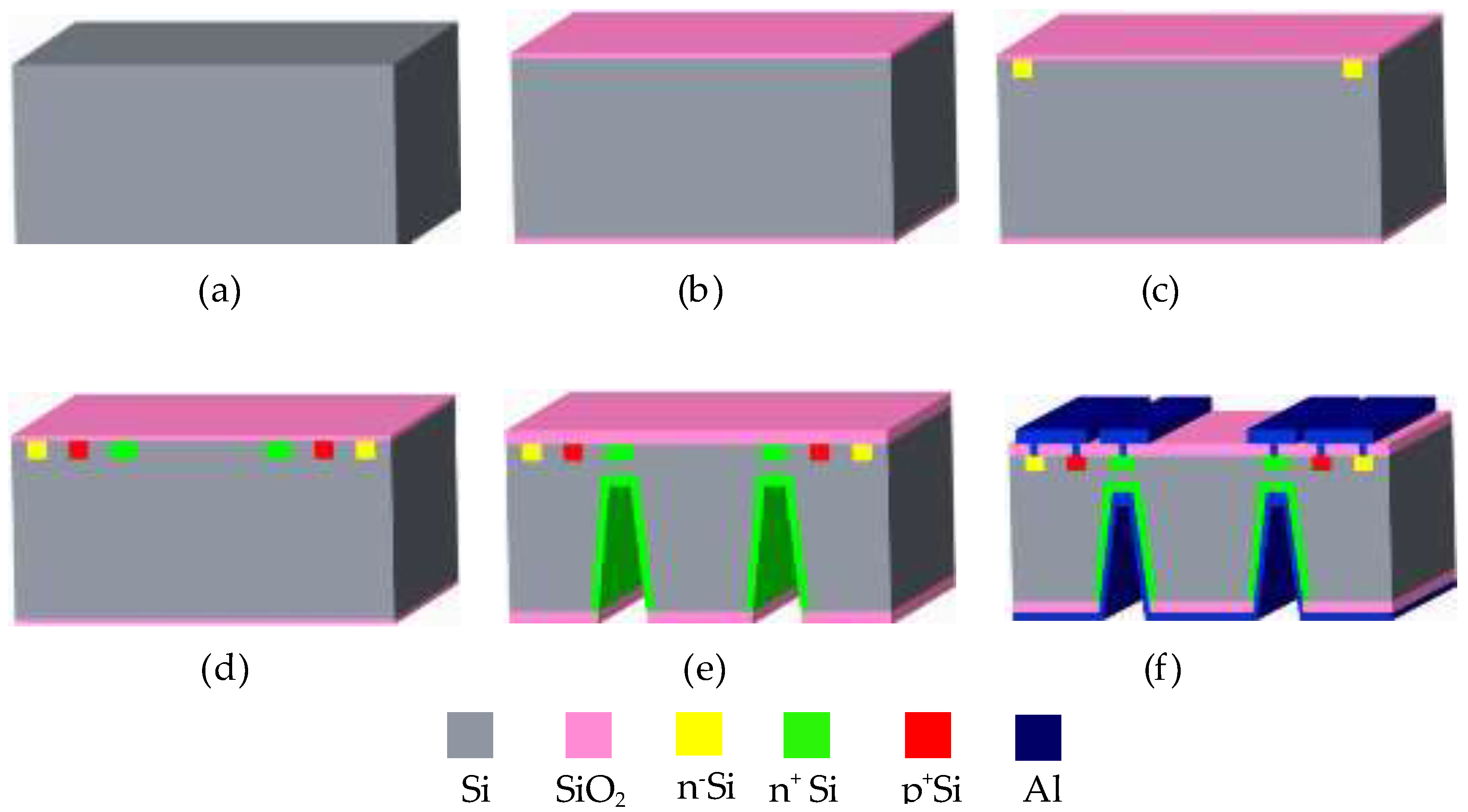
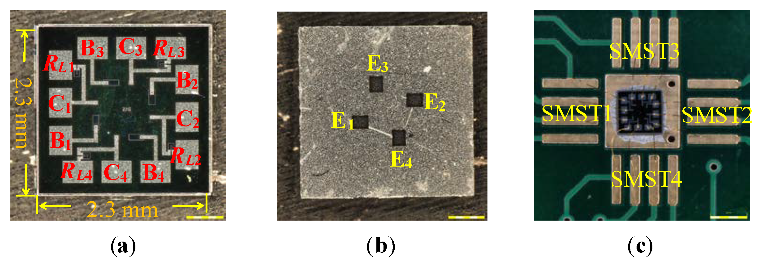
3. Fabrication Technology
4. Characteristics of the 2D Magnetic Field Sensor
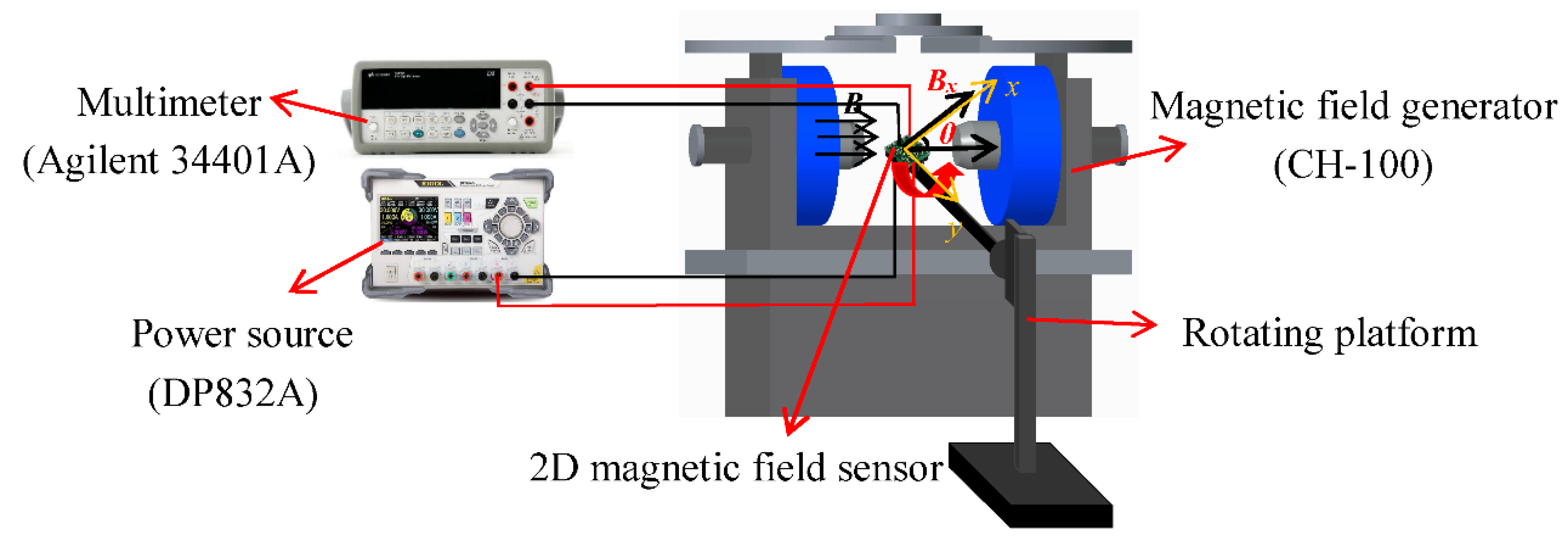
4.1. Testing System
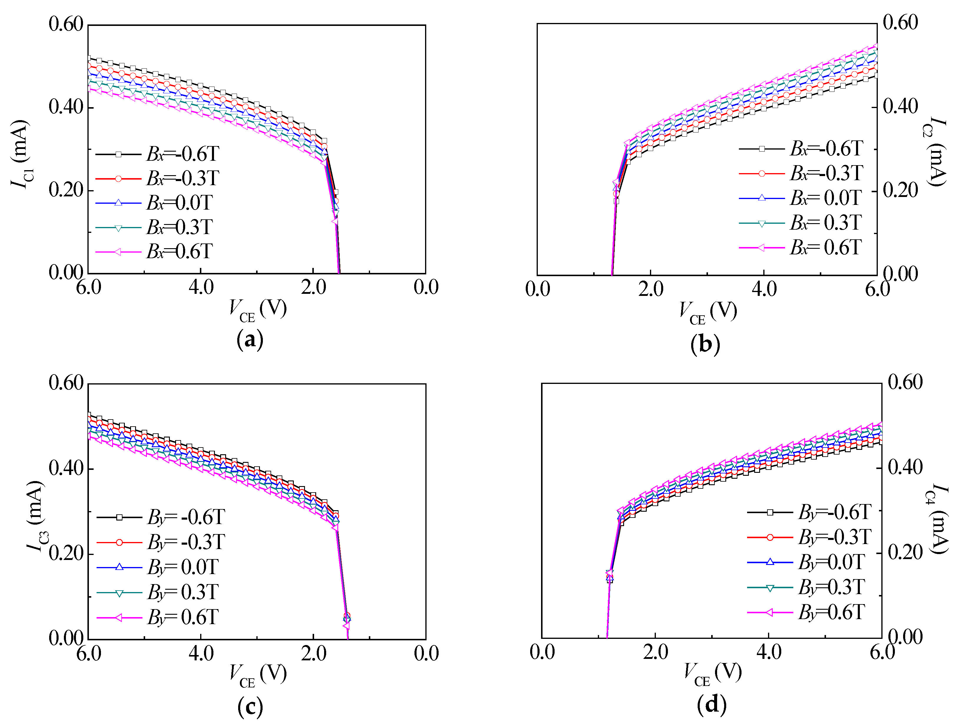
4.2. IC-VCE Characteristics of the SMSTs
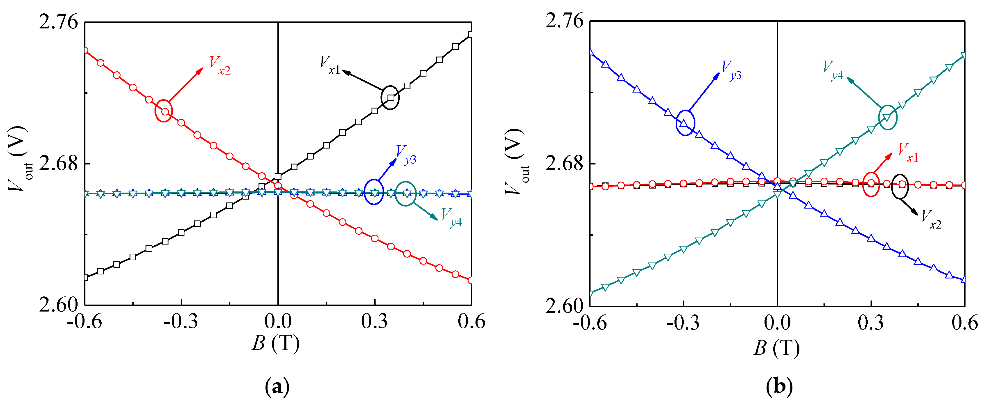
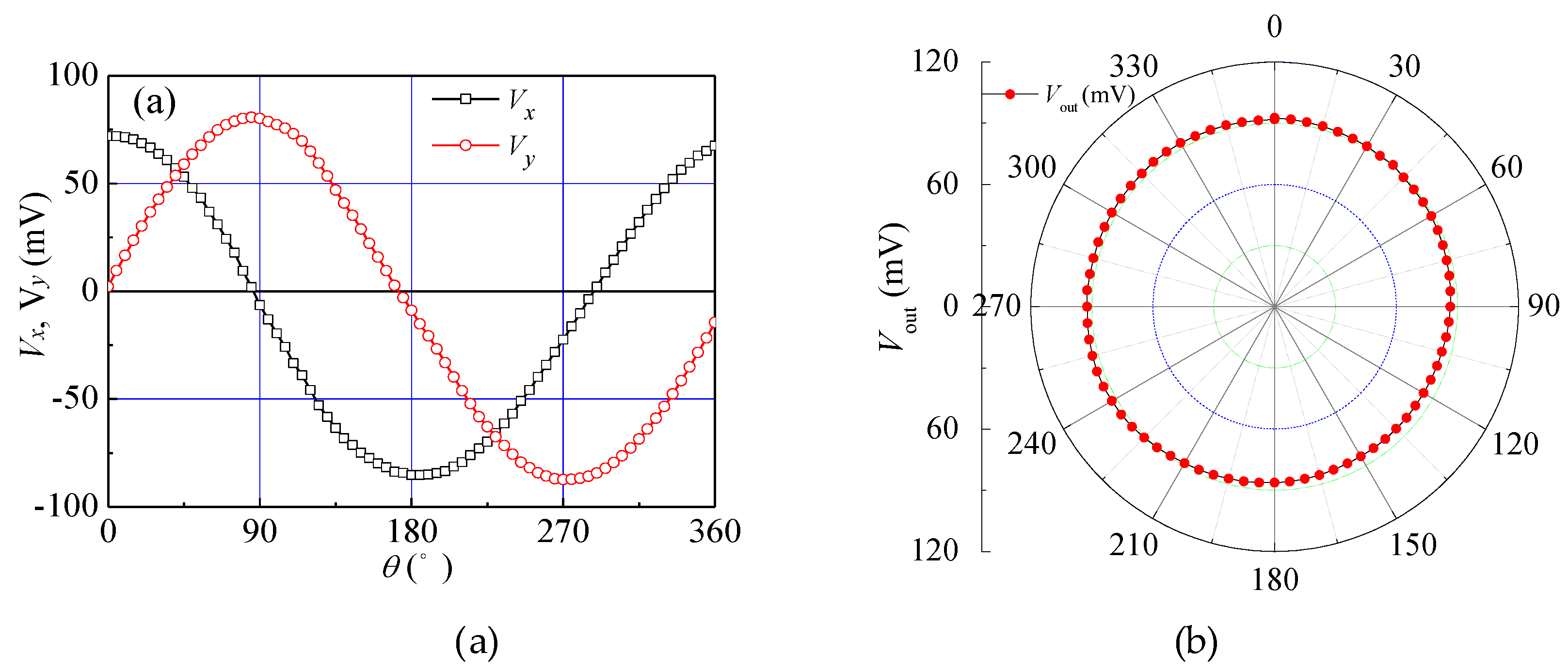
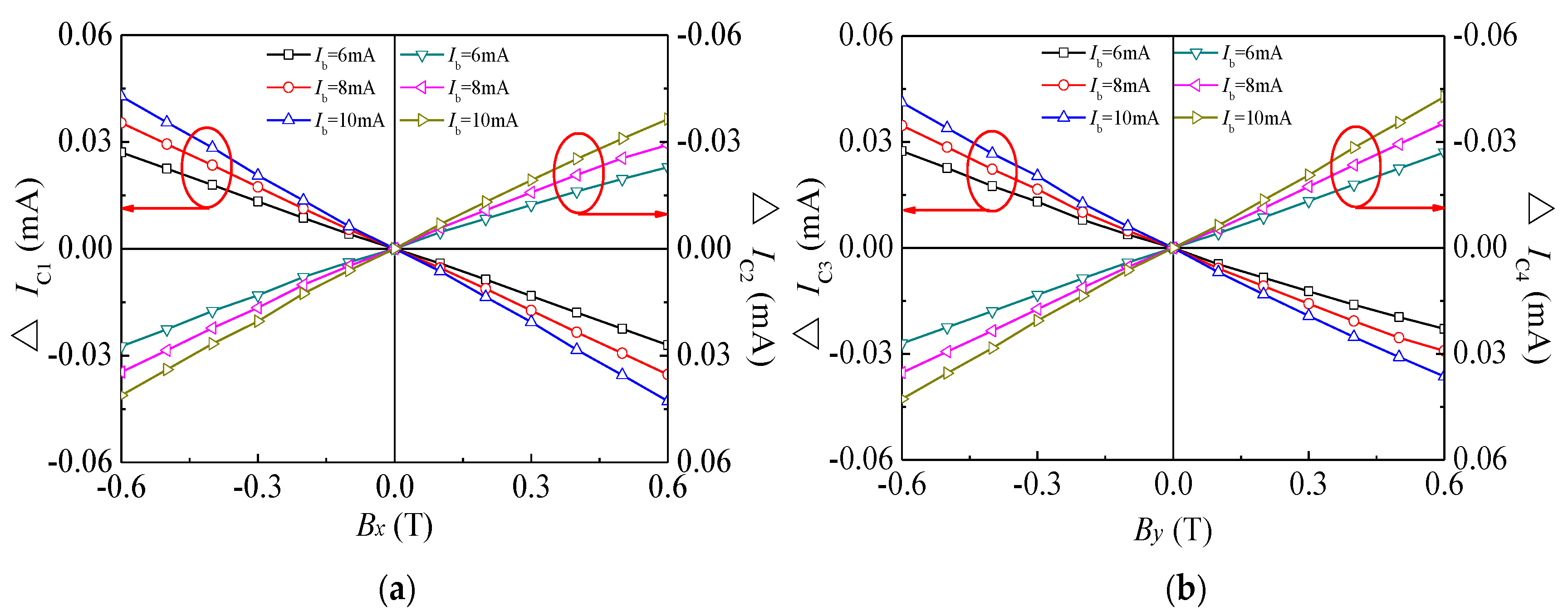
4.3. Magnetic Sensitivity Characteristics
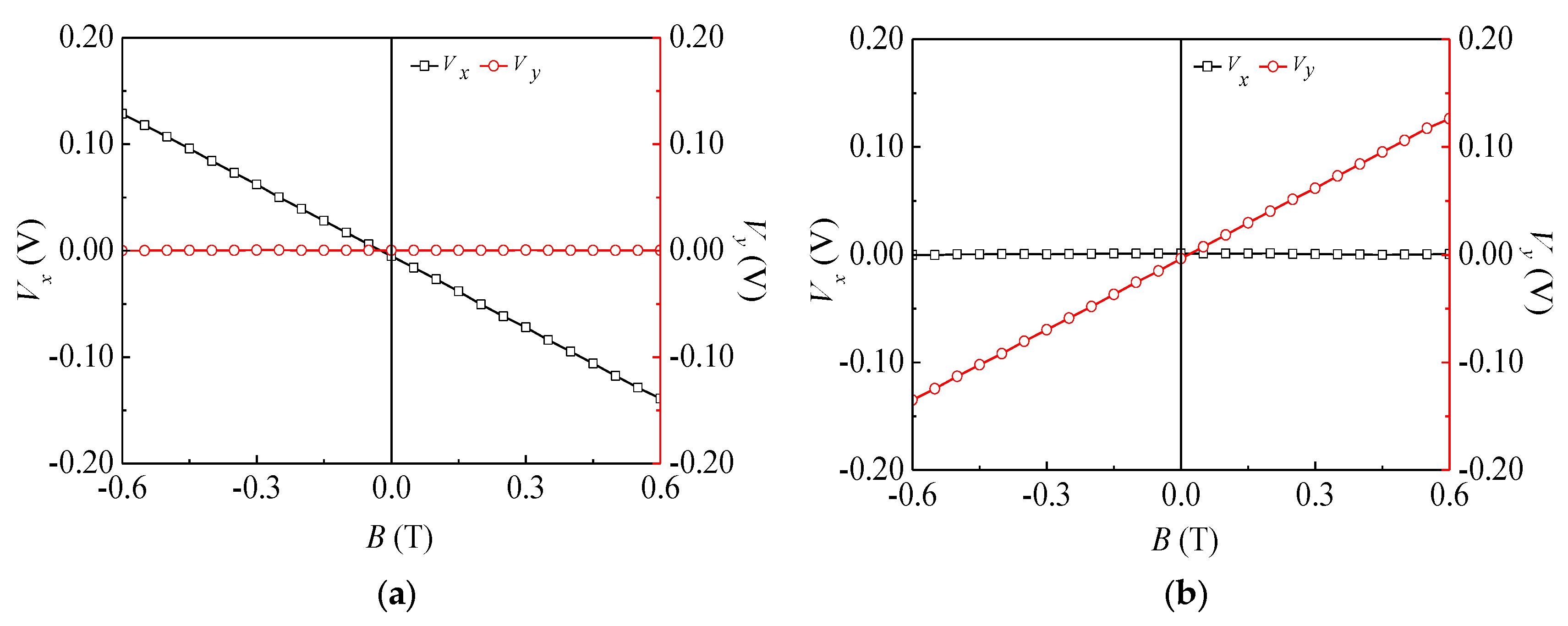
4.4. Characteristics of the 2D Magnetic Field Sensor
5. Conclusions
Author Contributions
Funding
Conflicts of Interest
References
- Roumenin, C.S.; Nikolov, D.; Ivanov, A. A novel parallel-field Hall sensor with low offset and temperature drift based 2D integrated magnetometer. Sens. Actuators A Phys. 2004, 115, 303–307. [Google Scholar] [CrossRef]
- Herrera-May, A.L.; Soler-Balcazar, J.C.; Vázquez-Leal, H.; Martínez-Castillo, J.; Vigueras-Zuñiga, M.O.; Aguilera-Cortés, L.A. Recent advances of MEMS resonators for lorentz force based magnetic field sensors: Design, Applications and Challenges. Sensors 2016, 16, 1359. [Google Scholar] [CrossRef] [PubMed]
- Zhao, X.F.; Li, B.Z.; Wen, D.Z. Fabrication technology and characteristics of a magnetic sensitive transistor with nc-Si:H/c-Si heterojunction. Sensors 2017, 17, 212. [Google Scholar] [CrossRef] [PubMed]
- Sander, C.; Leube, C.; Paul, O. Novel compact two-dimensional CMOS vertical Hall sensor. In Proceedings of the 2015 Transducers—2015 18th International Conference on Solid-State Sensors, Actuators and Microsystems (TRANSDUCERS), Anchorage, AK, USA, 21–25 June 2015; pp. 1164–1167. [Google Scholar]
- Roumenin, C.S. Magnetic sensors continue to advance towards perfection. Sens. Actuators A Phys. 1995, 46-47, 273–279. [Google Scholar] [CrossRef]
- DJiles, C.; Lo, C.C.H. The role of new materials in the development of magnetic sensors and actuators. Sens. Actuators A Phys. 2003, 106, 3–7. [Google Scholar]
- Banjevic, M.; Furrer, B.; Popovic, R.S. 2D CMOS integrated magnetometer based on the miniaturized circular vertical Hall device. In Proceedings of the 2009 International Solid-State Sensors, Actuators and Microsystems Conference, Denver, CO, USA, 21–25 June 2009; pp. 877–880. [Google Scholar]
- Zhao, X.F.; Wen, D.Z.; Zhuang, C.C.; Cao, J.; Wang, Z. Fabrication and characteristics of the magnetic field sensors based on nano-polysilicon thin-film transistors. J. Semicond. 2013, 34, 036001. [Google Scholar] [CrossRef]
- Yu, C.P.; Sung, G.M. Two-dimensional folded CMOS Hall device with interacting lateral magnetotransistor and magnetoresistor. Sens. Actuators A Phys. 2012, 182, 6–15. [Google Scholar] [CrossRef]
- Sung, G.M.; Yu, C.P. 2-D differential folded vertical Hall device fabricated on a P-Type substrate using CMOS technology. IEEE Sens. J. 2013, 13, 2253–2262. [Google Scholar] [CrossRef]
- Huang, H.Y.; Wang, D.J.; Xu, Y. A monolithic CMOS magnetic Hall sensor with high sensitivity and linearity characteristics. Sensors 2015, 15, 27359–27373. [Google Scholar] [CrossRef] [PubMed]
- Yang, X.H.; Zhao, X.F.; Bai, Y.J.; Wen, D. Two-Dimensional magnetic field sensor based on silicon magnetic sensitive transistors with differential structure. Micromachines 2017, 8, 95. [Google Scholar] [CrossRef]
- Lozanova, S.; Noykov, S.; Roumenin, C. Three-dimensional magnetometer based on subsequent measurement principle. Sens. Actuators A Phys. 2015, 222, 329–334. [Google Scholar] [CrossRef]


| Reference Parameters | Magnetic Sensitive Structure | Supply Voltage | Magnetic Sensitivity | Cross Interference | Chip Area |
|---|---|---|---|---|---|
| [9] | Hall device | 2.7 V | 9.56 mV/T | 0.259 mV (B = 150 mT) 0.330 mV (B = 150 mT) | 2.0 × 1.0 mm2 |
| [10] | Vertical Hall device | — | Sx = 40.06 mV/(V·T) Sy = 42.65 mV/(V·T) | 12.55 mV/(V·T) 12.33 mV/(V·T) | — |
| [11] | Hall device | 5.0 V | 34.0 mV/(V·T) | — | 60.0 × 60.0 μm2 |
| [12] | Magnetic sensitive transistor | VCE = 10.0 V IB = 6.0 mA | Sx = 366 mV/T Sy = 365 mV/T | — | 7.0 × 7.0 mm2 |
| This work | Magnetic sensitive transistor | VCE = 5.0 V IB = 8.0 mA | Sx = 223 mV/T Sy = 218 mV/T | 0.19% 0.04% | 2.3 × 2.3 mm2 |
© 2018 by the authors. Licensee MDPI, Basel, Switzerland. This article is an open access article distributed under the terms and conditions of the Creative Commons Attribution (CC BY) license (http://creativecommons.org/licenses/by/4.0/).
Share and Cite
Zhao, X.; Jin, C.; Deng, Q.; Lv, M.; Wen, D. Fabrication Technology and Characteristics Research of a Monolithically-Integrated 2D Magnetic Field Sensor Based on Silicon Magnetic Sensitive Transistors. Sensors 2018, 18, 2551. https://doi.org/10.3390/s18082551
Zhao X, Jin C, Deng Q, Lv M, Wen D. Fabrication Technology and Characteristics Research of a Monolithically-Integrated 2D Magnetic Field Sensor Based on Silicon Magnetic Sensitive Transistors. Sensors. 2018; 18(8):2551. https://doi.org/10.3390/s18082551
Chicago/Turabian StyleZhao, Xiaofeng, Chenchen Jin, Qi Deng, Meiwei Lv, and Dianzhong Wen. 2018. "Fabrication Technology and Characteristics Research of a Monolithically-Integrated 2D Magnetic Field Sensor Based on Silicon Magnetic Sensitive Transistors" Sensors 18, no. 8: 2551. https://doi.org/10.3390/s18082551
APA StyleZhao, X., Jin, C., Deng, Q., Lv, M., & Wen, D. (2018). Fabrication Technology and Characteristics Research of a Monolithically-Integrated 2D Magnetic Field Sensor Based on Silicon Magnetic Sensitive Transistors. Sensors, 18(8), 2551. https://doi.org/10.3390/s18082551