A Compact and Low Power RO PUF with High Resilience to the EM Side-Channel Attack and the SVM Modelling Attack of Wireless Sensor Networks


Abstract
1. Introduction
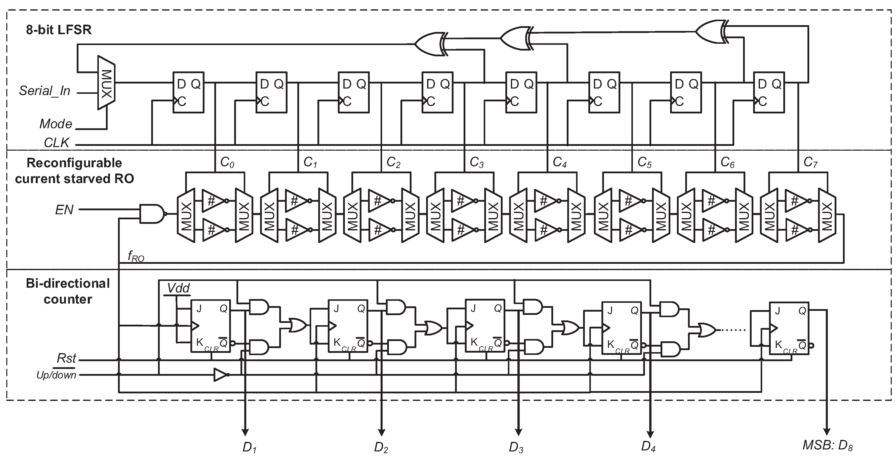
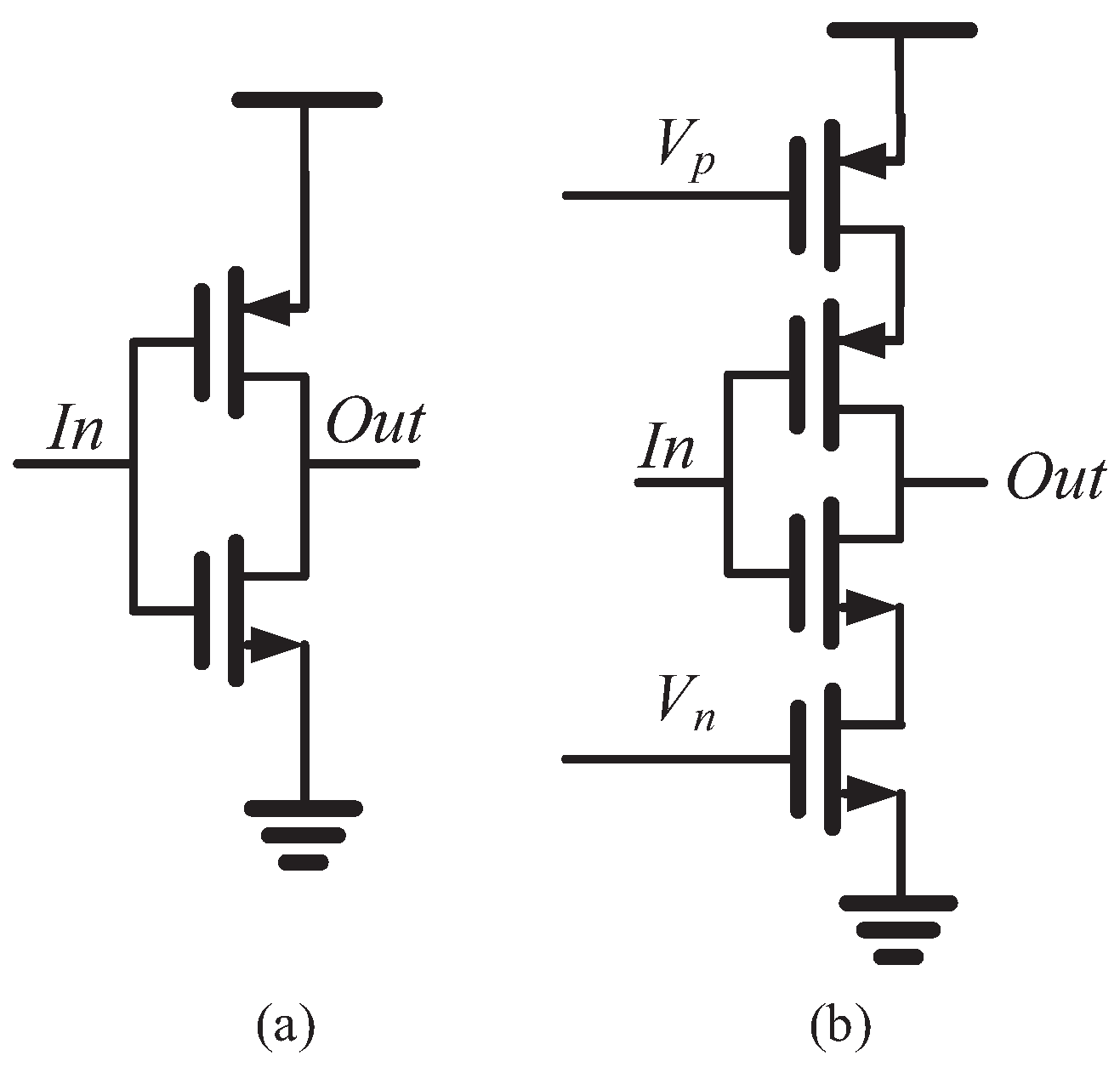
2. Architecture and Operation of Proposed RO PUF
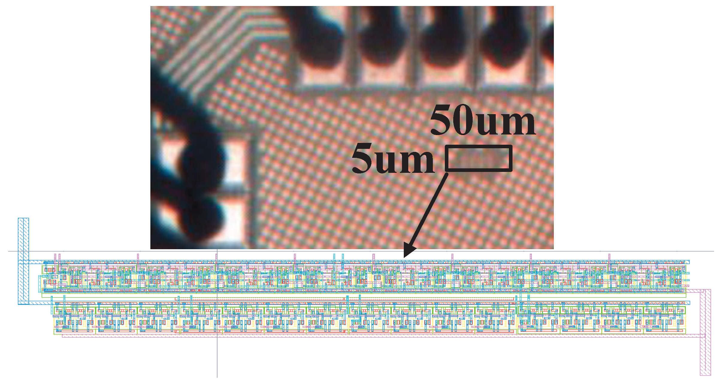
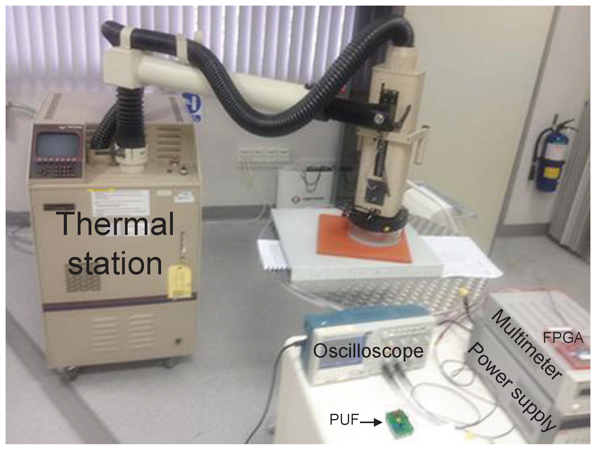
3. Experimental Results and Discussions
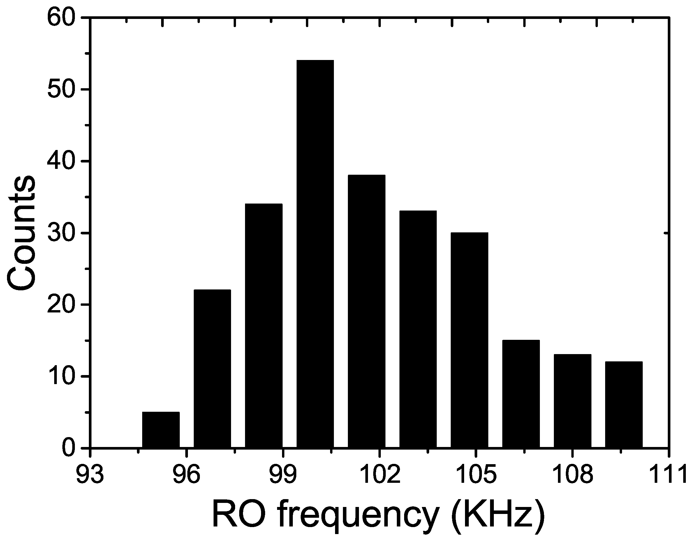
3.1. Uniqueness
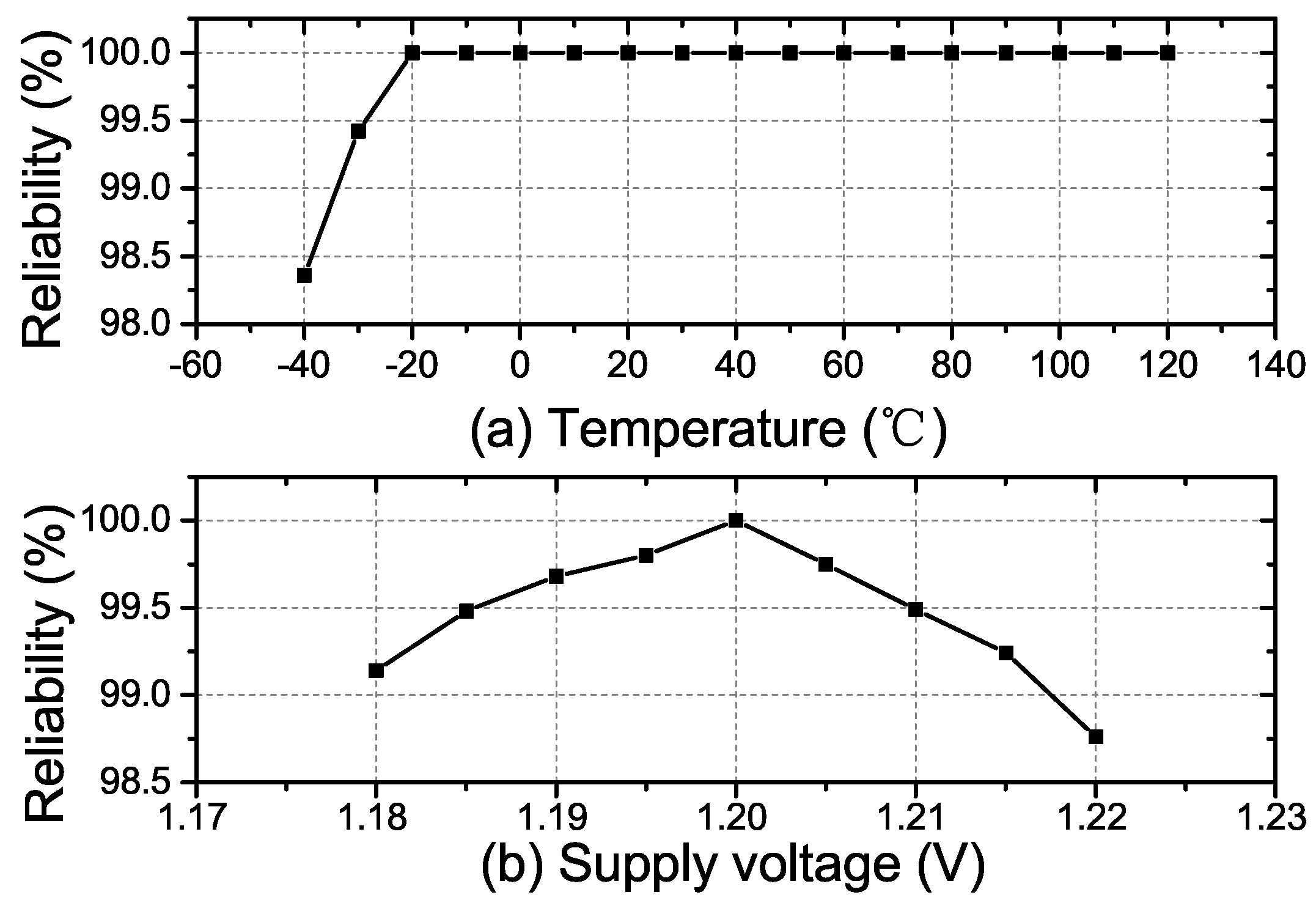
3.2. Reliability
3.3. Power Consumption
3.4. Security Analysis
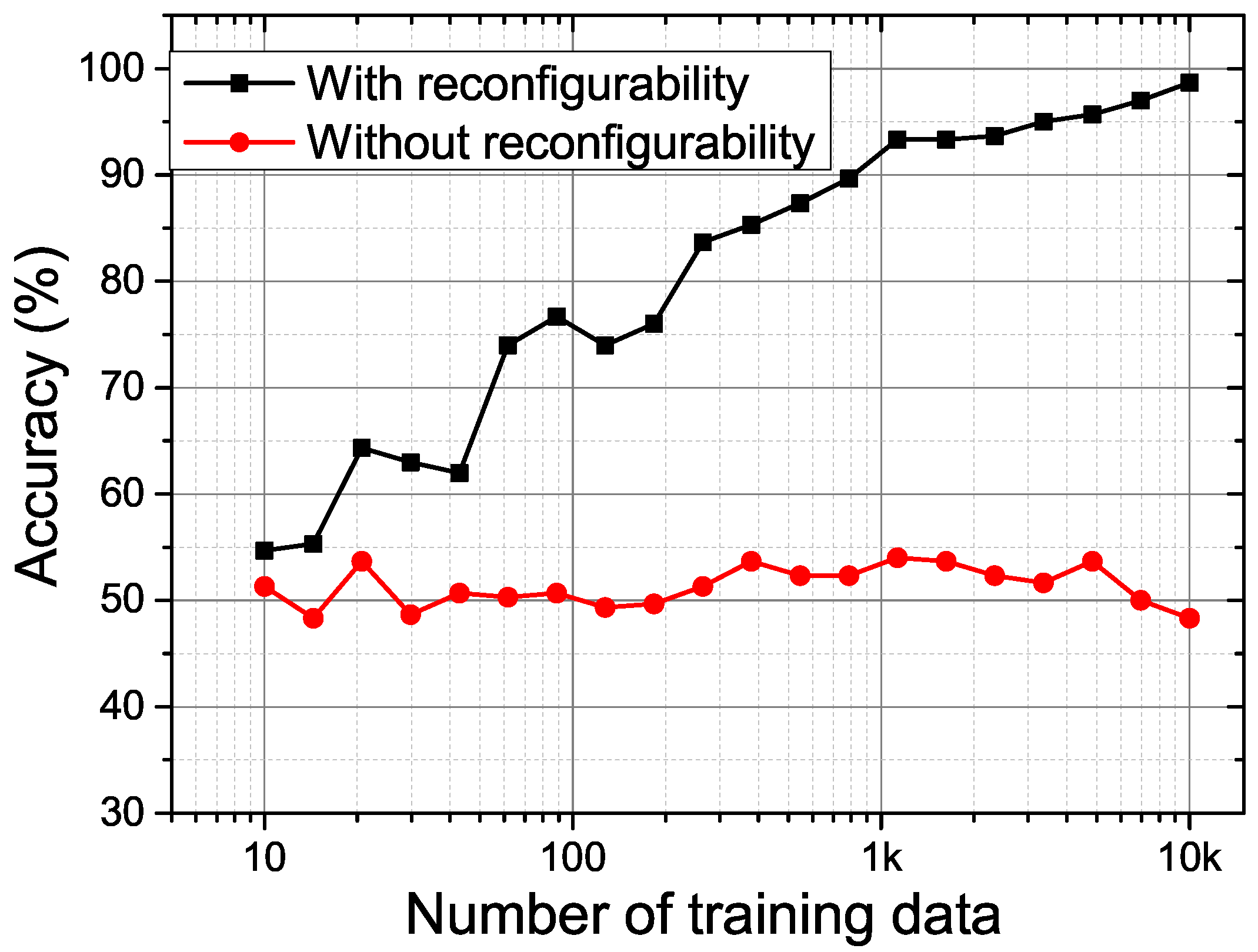
3.4.1. SVM Attack
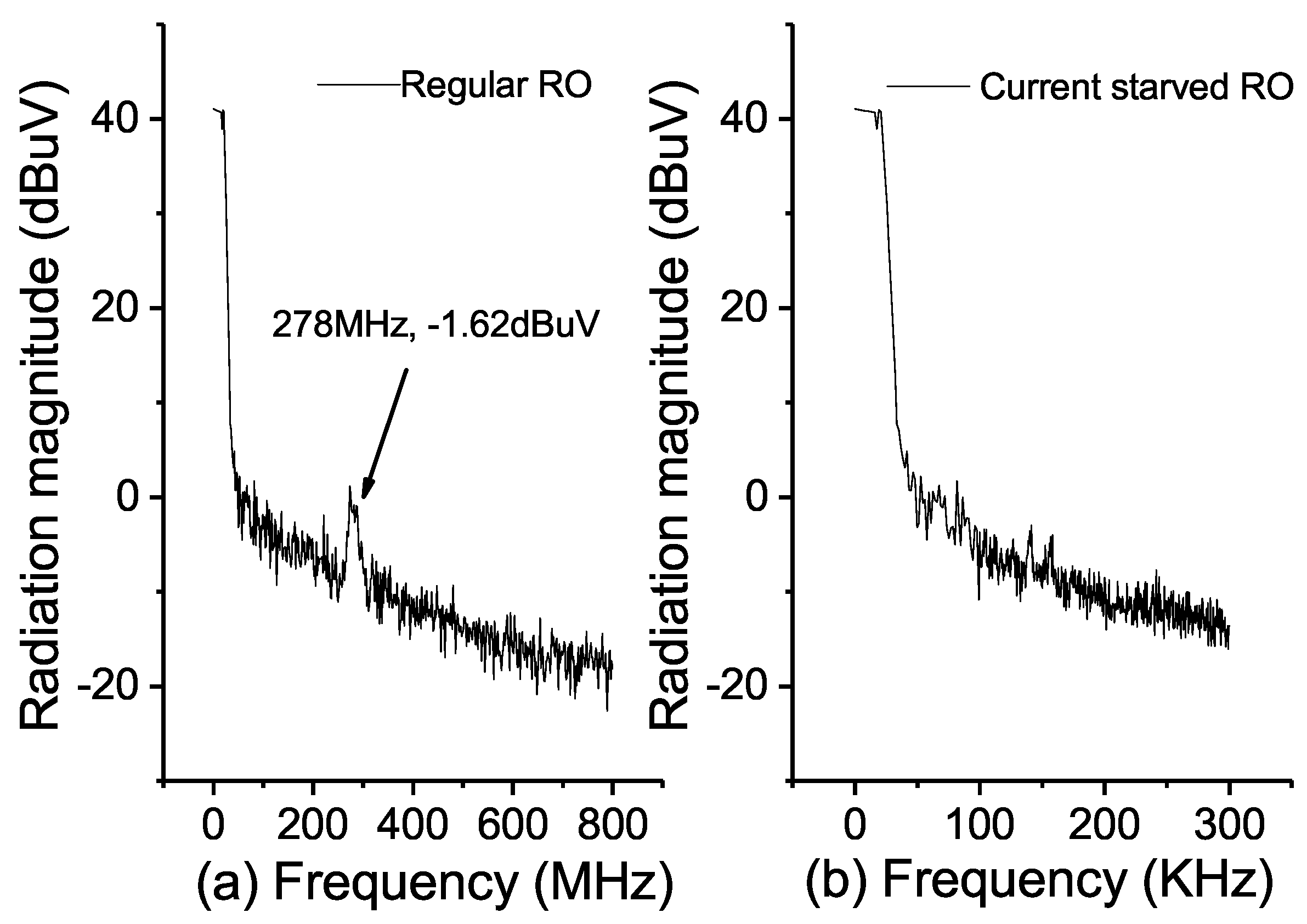
3.4.2. EM Side-Channel Attack
4. Conclusions
Acknowledgments
Author Contributions
Conflicts of Interest
References
- Ergen, S.C.; Sangiovanni-Vincentelli, A. Intravehicular energy-harvesting wireless networks: Reducing costs and emissions. IEEE Veh. Technol. Mag. 2017, 12, 77–85. [Google Scholar] [CrossRef]
- Liu, R.; Wu, H.; Pang, Y.; Qian, H.; Yu, S. Experimental characterization of physical unclonable function based on 1 kb resistive random access memory arrays. IEEE Electron Device Lett. 2015, 36, 1380–1383. [Google Scholar] [CrossRef]
- Li, D.; Lu, Z.; Zou, X.; Liu, Z. PUFKEY: A high-security and high-throughput hardware true random number generator for sensor networks. Sensors 2015, 15, 26251–26266. [Google Scholar] [CrossRef] [PubMed]
- Kim, M.S.; Moon, D.I.; Yoo, S.K.; Lee, S.H.; Choi, Y.K. Investigation of physically unclonable functions using flash memory for integrated circuit authentication. IEEE Trans. Nanotechnol. 2015, 14, 384–389. [Google Scholar] [CrossRef]
- Das, J.; Scott, K.; Rajaram, S.; Burgett, D.; Bhanja, S. MRAM PUF: A novel geometry based magnetic PUF with integrated CMOS. IEEE Trans. Nanotechnol. 2015, 14, 436–443. [Google Scholar] [CrossRef]
- Chen, A. Utilizing the variability of resistive random access memory to implement reconfigurable physical unclonable functions. IEEE Electron Device Lett. 2015, 36, 138–140. [Google Scholar] [CrossRef]
- Li, J.; Seok, M. Ultra-compact and robust physically unclonable function based on voltage-compensated proportional-to-absolute-temperature voltage generators. IEEE J. Solid-State Circuits 2016, 51, 2192–2202. [Google Scholar] [CrossRef]
- Rührmair, U.; Sölter, J.; Sehnke, F.; Xu, X.; Mahmoud, A.; Stoyanova, V.; Dror, G.; Schmidhuber, J.; Burleson, W.; Devadas, S. PUF modeling attacks on simulated and silicon data. IEEE Trans. Inf. Forensics Secur. 2013, 8, 1876–1891. [Google Scholar] [CrossRef]
- Yang, K.; Dong, Q.; Blaauw, D.; Sylvester, D. A physically unclonable function with BER <10−8 for robust chip authentication using oscillator collapse in 40 nm CMOS. In Proceedings of the 2015 IEEE International Solid State Circuits Conference, San Francisco, CA, USA, 22–26 February 2015; pp. 1–3. [Google Scholar]
- Komurcu, G.; Pusane, A.; Dundar, G. Analysis of ring oscillator structures to develop a design methodology for RO-PUF circuits. In Proceedings of the International Conference on Very Large Scale Integration (VLSI-SoC), Istanbul, Turkey, 7–9 October 2013; pp. 332–335. [Google Scholar]
- Lin, L.; Srivathsa, S.; Krishnappa, D.K.; Shabadi, P.; Burleson, W. Design and validation of arbiter-based PUFs for sub-45-nm low-power security applications. IEEE Trans. Inf. Forensics Secur. 2012, 7, 1394–1403. [Google Scholar] [CrossRef]
- Merli, D.; Heyszl, J.; Heinz, B.; Schuster, D.; Stumpf, F.; Sigl, G. Localized electromagnetic analysis of RO PUFs. In Proceedings of the Hardware-Oriented Security and Trust (HOST), Austin, TX, USA, 2–3 June 2013; pp. 19–24. [Google Scholar]
- Taur, Y.; Ning, T. Fundamentals of Modern VLSI Devices; Cambridge University Press: Cambridge, UK, 1998. [Google Scholar]
- Mondal, S.; Talapatra, S.; Rahaman, H. Analysis, modeling and optimization of transmission gate delay. In Proceedings of the Asia Symposium on Quality Electronic Design (ASQED), Kuala Lumpur, Malaysia, 19–20 July 2011; pp. 246–253. [Google Scholar]
- Katzenbeisser, S.; Koçabas, Ü.; Van Der Leest, V.; Sadeghi, A.R.; Schrijen, G.J.; Schröder, H.; Wachsmann, C. Recyclable PUFs: Logically reconfigurable PUFs. J. Cryptogr. Eng. 2011, 1, 177–186. [Google Scholar] [CrossRef]
- Gassend, B.; Clarke, D.; Van Dijk, M.; Devadas, S. Silicon physical random functions. In Proceedings of the ACM Conference on Computer and Communications Security, Washington, DC, USA, 18–22 November 2002; pp. 148–160. [Google Scholar]
- Maiti, A.; Schaumont, P. Improving the quality of a Physical Unclonable Function using configurable Ring Oscillators. In Proceedings of the International Conference on Field Programmable Logic and Applications, Prague, Czech Republic, 31 August–2 September 2009; pp. 703–707. [Google Scholar]
- Ramazani, A.; Biabani, S.; Hadidi, G. CMOS ring oscillator with combined delay stages. Int. J. Electron. Commun. 2014, 68, 515–519. [Google Scholar] [CrossRef]
- Joachims, T. Learning to classify text using support vector machines: Methods, theory and algorithms. Comput. Linguist. 2003, 29, 655–664. [Google Scholar]
- Hogg, D. Fun with the Friis free-space transmission formula. IEEE Antennas Propag. Mag. 1993, 35, 33–35. [Google Scholar] [CrossRef]
- He, W.; de la Torre, E.; Riesgo, T. An interleaved EPE-immune PA-DPL structure for resisting concentrated EM side channel attacks on FPGA implementation. In Proceedings of the International Conference on Constructive Side-Channel Analysis and Secure Design (COSADE), Darmstadt, Germany, 3–4 May 2012; pp. 39–53. [Google Scholar]


© 2018 by the authors. Licensee MDPI, Basel, Switzerland. This article is an open access article distributed under the terms and conditions of the Creative Commons Attribution (CC BY) license (http://creativecommons.org/licenses/by/4.0/).
Share and Cite
Cao, Y.; Zhao, X.; Ye, W.; Han, Q.; Pan, X. A Compact and Low Power RO PUF with High Resilience to the EM Side-Channel Attack and the SVM Modelling Attack of Wireless Sensor Networks. Sensors 2018, 18, 322. https://doi.org/10.3390/s18020322
Cao Y, Zhao X, Ye W, Han Q, Pan X. A Compact and Low Power RO PUF with High Resilience to the EM Side-Channel Attack and the SVM Modelling Attack of Wireless Sensor Networks. Sensors. 2018; 18(2):322. https://doi.org/10.3390/s18020322
Chicago/Turabian StyleCao, Yuan, Xiaojin Zhao, Wenbin Ye, Qingbang Han, and Xiaofang Pan. 2018. "A Compact and Low Power RO PUF with High Resilience to the EM Side-Channel Attack and the SVM Modelling Attack of Wireless Sensor Networks" Sensors 18, no. 2: 322. https://doi.org/10.3390/s18020322
APA StyleCao, Y., Zhao, X., Ye, W., Han, Q., & Pan, X. (2018). A Compact and Low Power RO PUF with High Resilience to the EM Side-Channel Attack and the SVM Modelling Attack of Wireless Sensor Networks. Sensors, 18(2), 322. https://doi.org/10.3390/s18020322