1. Introduction
In recent years, Indium(III) oxide (In
2O
3) has shown a potential as a promising new material for gas sensing applications, in particular suitable for the detection of low concentrations of oxidizing gases like O
3, NO
x, and Cl
2 [
1,
2,
3,
4]. On the other hand, it was also shown that In
2O
3-based gas sensors may have sufficient sensitivity and good selectivity toward some reducing gases (such as CO or H
2) [
5,
6], this latter property strongly depending on the preparation route and surface stoichiometry. In fact, it is known that sensing performance of a metal oxides sensor is mainly regulated by its microscopic morphology and defect chemistry, material properties largely depending on the manufacturing process. In this regard, performance of gas sensors has been shown to be really boosted by using nano-structured materials [
1,
2,
3,
6].
In past, In
2O
3 nano-structured films have been manufactured by many different techniques such as chemical vapor deposition, thermal oxidation of In films, spray pyrolysis, sol–gel, atomic layer deposition, pulsed laser ablation, DC, and RF-sputtering [
7]. These techniques generally require a complex processing for precursors to be formed in the environment of the deposition chamber. Furthermore, they require rather high temperatures of the substrate, and therefore generally do not allow using substrates already equipped with screen printed circuitry, as in the case of gas sensing devices, which will be damaged or even melted by high temperatures.
In particular, papers by Korotcenkov et al. (e.g., [
8,
9]), studied deeply the behavior of In
2O
3 sensors grown by spray pyrolysis, discussing thoroughly the influence of the sensor microstructure on their performance.
In this work, we deposited nano-crystalline layers of In2O3 on dedicated printed circuit boards (PCBs). We used a novel deposition method, the low temperature pulsed electron deposition (LPED) technique, where a pulsed high power electron beam, permitting the non-equilibrium extraction of energetic particles, allows for depositing homogeneous films with the proper stoichiometry of almost any kind of materials at ambient temperatures, so that direct deposition on temperature-sensitive substrates as PCBs is made possible. In particular, for the sensors presented in this paper the LPED technique was applied with the simultaneous measurement of the film resistance during the growth, which is a specific and novel characteristic of our deposition procedure.
Based on previous works from Korotcenkov, we analyzed and modeled the behavior of our In
2O
3 nano-films deposited by LPED as NO
x and CO sensors. Two models are compared to discuss the behavior of our sensors, one where a ‘dense’ thin film is taken into account, and the other where ‘porous’ films are considered, this latter as already modeled in [
10]. The comparison led to the conclusion that, for film thicknesses which bring to reasonable values for the film resistance, the ‘dense’ thin film model is the one that best fits the experimental results, which are in agreement with the ones reported by Korotcenkov in [
9]. In particular, reducing the film thickness and the grain size decreases the time constants of the gas response of In
2O
3-based gas sensors, and increases the response to oxidizing gases (thanks also to an increased gas permeability of the film).
3. Experimental Results
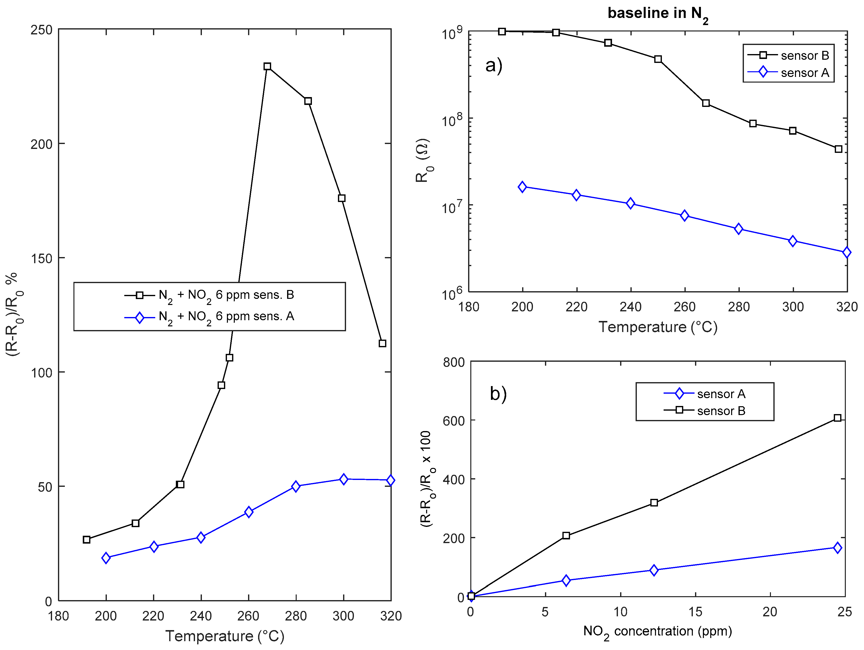
The characterization results for sensors obtained after a deposition of 4 h (thickness around 150 nm) are summarized in
Figure 10, where the response to CO and NO
2 are shown. Moreover, in the figure the baseline resistance values in the two carrier gases are plotted as a function of temperature. As expected, the material behaves as an n-type semiconductor, and responds with an increased resistance to the oxidizing gases. The behavior in air and nitrogen is similar: oxygen seems to have little influence on the response to NO
2 at high temperatures. Due to the material properties discussed in the introduction, the sensor shows a satisfactory response to NO
2 (60% @ 6 ppm NO
2 @ 320 °C in dry air). The response to NO
2 in the tested concentration interval is fairly linear, both in nitrogen and in air. This behavior will be justified later by the proposed model. On the other hand, the sensor exhibits a negligible response to CO, which shows an anomalous behavior as acceptor-like extrinsic surface state (see
Figure 10). This behavior, for the same temperature interval and in case of nano-grained thin films (thickness < 200 nm), was already described and discussed in [
8].
In detail, it was found that CO always behaves as an acceptor like extrinsic surface state in N
2 carrier gas, whereas in oxygen a reducing behavior is superimposed to the oxidizing behavior but only at high temperature. In [
19], the acceptor-like behavior of CO was explained through the presence of humidity and oxygen in the environment. The experimental results seem only partially in agreement with this hypothesis, in fact using the dry inert gas carrier this anomalous behavior is still observable.
The low sensitivity to CO and the small variation of the baseline resistance (see
Figure 10) can be both explained by the absence of the depleted region at the surface. Nevertheless, also a small reactivity of the oxygen deficient surface with CO can be hypothesized. This last possible explanation is supported by measurements performed with a quartz crystal microbalance (AT-cut 10 MHz) at room temperature on whose gold electrodes a nano-layer (<100 nm thickness) of In
2O
3 was deposited with the same technique [
20]. This sensor has a very little response to CO (no measureable response up to 2000 ppm CO), whereas it senses 12 ppm NO
2.
The response of the sensors is highly dependent on the deposition time, i.e., on the layer geometry and film aspect ratio (
Figure 11). Both the response and the speed of the sensor are beneficiated by a reduction of the sensor thickness; the drawback of reducing the deposition time is the reduction of the surface area and the very large value of the resistance that is obtained with deposition times shorter than 2 h.
In
Figure 12 the transient responses to NO
2 of two sensors obtained with different deposition times are compared: it can be seen that reducing the deposition from 4 h time to 2 h (thickness about 70 nm), the response speed is highly improved, in fact the thinner sensor (sensor B) reaches the steady state and completely recovers in 4 min at temperatures larger than 290 °C.
4. Sensor Model for Oxidizing Gas
In general, in semiconductor metal oxides, gas sensing is mainly performed through three possible mechanisms affecting the electrical resistance (R):
(a) Change of free charge carrier concentration (n), due to capture/release at adsorbed species on surface, R ∝ 1/n.
(b) Change of potential barrier height (
qVs) at the crystal domain (or grain) boundary, due to the presence of ionized adsorbed species on the crystallites surface. Barrier is due to charge carriers trapping at surface by acceptor surface states. The density of acceptor ionized surface states is determined by the population of intrinsic surface defects and by the possible presence of chemisorbed molecules. This gives rise to an exponential dependence of the electrical resistance on the barrier height, which is approximately related to the square of the trapped charge surface density:
R ∝
exp(
qVs/kT). The barrier height depends also on native acceptor surface defects (for n-type semiconductors) and on the concentration of the surrounding gas (oxidizing gas favoring the barrier, reducing gases likely suppressing it). On the contrary, if on the surface there are donor-like defects, a carrier enriched surface layer exists and the dependence of
R on the charge surface density is no more exponential [
20,
21].
(c) Change of bulk electronic properties, such as the donor concentration (Nd) and bulk charge carriers mobility (μn), in this latter case R ∝ 1/(Nd μn).
The first two mechanisms are pure surface phenomena driven by the adsorption/desorption of the surrounding gas and by the ionization/neutralization of adsorbed species. Obviously, diffusion toward the intergrain/boundary regions can also play a role in the kinetics.
The third process is a red/ox of the lattice, and takes into account possible diffusion of charged species in the bulk. According to [
5], in In
2O
3 this last phenomenon seems to be negligible at temperatures lower than 350 °C.
Usually the most relevant phenomenon causing an exponential dependence of the resistance on the surface density of chemisorbed molecules is the (b) one. Compared with other well-known metal oxides (such as SnO
2), In
2O
3 has a more complicated behavior as a gas sensor, due to the fact that the surface oxygen stoichiometry (oxygen deficiency) is such that the native surface defects may have a donor character. For this reason, it is possible that in reducing gases the surface is oxidized and no depleted region is formed at the surface of crystallites or grains, (on the contrary, there is a carrier enriched surface even in the presence of air [
21,
22], whereas in oxidizing environments a depleted region appears and the sensor behavior is the usual barrier height dependent one (b) [
23]).
It is known, that when the grain/film size goes below a certain critical value the influence of the grain/film geometry becomes important, and strongly influences the sensor response. In some previous works, the case of a thick film porous film made up of nano-spheres was treated by the authors and applied both to p-type and n-type materials [
10,
24]. The same model can be used also for thin films when they consist of loosely bound grains (porous layer) as shown in
Figure 13a. This model could be used also for the thin nano-film described in this paper when short deposition times are used. Nevertheless, to ensure a reasonable value for the film resistance, as discussed in the previous section, the deposition has to be longer than 1.5 h. For long deposition time the film can become ‘dense’ (see
Figure 13b). Assuming that no intrinsic acceptor like surface defect can be found at the grain boundary, such that no potential barrier exists at the grain interface, a possible model for the film is the compact thin-layer shown in
Figure 13c. Moreover, Rombach in [
23] showed that the vertical domain boundaries in the textured films have no detectable influence on the sensing behavior. In this case, the variation of resistance can be ascribed to the reduction of the current path cross section area, related to the creation of a depleted region on the surface when an oxidizing gas is present.
Let us consider a thin film of homogeneous material exposed to a mixture of air and NO
2 (oxidizing gas); at the surface the two following chemisorption reactions are expected.
where (
X-Sx)
− indicates an adsorbed and negatively ionized molecule of the species
X at the adsorption site
Sx, and
e− indicates a free electron at the surface.
As a whole, the amount of charge localized at the surface is due both to intrinsic ionized defects and to the chemisorbed molecules with a total surface charge density −
qNs, being
q the electron charge and
Ns the total negatively charged species density that can be written as [
1,
25,
26,
27]
where
Ni indicates the density of ionized intrinsic defects that can be either acceptors or donors (actually, the surface of semiconductors tends always to be depleted [
10]), and [
X] indicates the surface density of the species
X. In this work, we consider to have only extrinsic acceptor surface states due to the adsorption of both atomic oxygen and of the target gas NO
2, a net negative charge, so that
Ns cannot usually assume a negative sign.
Due to the trapped surface charge we expect that, when the equilibrium is reached, an electric field establishes in the grain to counterbalance the diffusion of free carriers which reach the surface from the bulk. We take into account an n-type semiconductor where the bulk free electron density is
Nd and the hole density is negligible. We consider a depleted surface—i.e., to have a net negative charge trapped at the surface—so that −
qNs, the charge density, is negative and uniform on the surface. The positive charge density,
ρ, in the film at the thermal equilibrium can be found by balancing the diffusion current related to the charge density gradient and the free electron drift current caused by the electric field. With reference to the geometry shown in
Figure 14, being
t <<
b and
t <<
l, considering a homogeneous thin film and a uniform charge density at the surface, all the quantities can be considered to depend only on the of the z coordinate. Hence, the charge density can be found from the equation
where
Jtot(
z) is the current density,
Ez(
z) the electrical field,
σn =
qn(
z)
μn is the conductivity (
μn is the free electron mobility),
Dn is the diffusion coefficient of free electrons (
Dn =
μn kT/
q), and
n(
z) is the free electrons density in the bulk.
Usually, the positive charge density in the depleted layer,
ρ(
z), is considered to be constant and equal to
qNd (full depletion) so that in this layer no free electrons exist. Instead, we consider a spatial distribution of the charge that can be related to the free carrier density in this layer as
From Equation (6) the conductivity in the depleted layer can be written as
moreover
where
ε is the electric permittivity.
Replacing the expressions in Equations (6)–(8) in Equation (5) we obtain the following integral-differential equation
where 0 ≤
ρ(
z) ≤
qNd holds, and
ρ(0) assumes a value granting the following electro-neutrality condition
Equation (9) can be rewritten as
By numerically solving Equation (11) the charge density, the electrical field and the voltage distribution in the layer can be found.
It could be noted that since
ρ(
z) is always an increasing function of
z, its local slope is determined by the length
Therefore, it can be shown (see other works of the authors, e.g., [
10,
24]) that if the thickness of the layer is not much larger than the minimum value of
λ given by the rightmost term of the inequality in Equation (12),
ρ(
z) slowly varies along z and its behavior is very far from the ‘fully depleted layer approximation’. It is evident that this condition is exactly equivalent to the usual condition
with
being the Debye length.
When an external electrical field
Eext is applied along the axis x, and considering it so small as not to interfere with the equilibrium due to the chemisorption, the following relationship holds for the drift current
Jx(
z)
Hence the resistance of the layer can be found evaluating the following integral
Actually, being the electro-neutrality condition (Equation (10)) always true, this integral is simply equal to
Hence, if
G =
G(
Ns) is the conductance of the film in presence of the target gas, whereas
G0 =
G(
Ns0) is the conductance of the film in a reference condition, for instance in the carrier gas, we have
and, for the sensor response as defined in Equation (2)
So for the dense compact film a linear relationship between the charged species density and the conductance is expected. It can be seen that the sensor response depends on the film thickness and on the bulk carrier density. The smaller are these quantities the larger the sensor response. So, very thin pure films would provide, in principle, very good sensitivities. Obviously, both thickness and bulk carrier density cannot be pushed to low values limitless because they determine the film resistance value. A lower limit for both is set by the maximum measureable resistance and by the desired measurement range. In particular, very large resistances lead to heavy problems in measurement system design, and limit the measurement accuracy. Moreover, a low Nd value and a small thickness can bring to the depletion of the entire film and to response saturation.
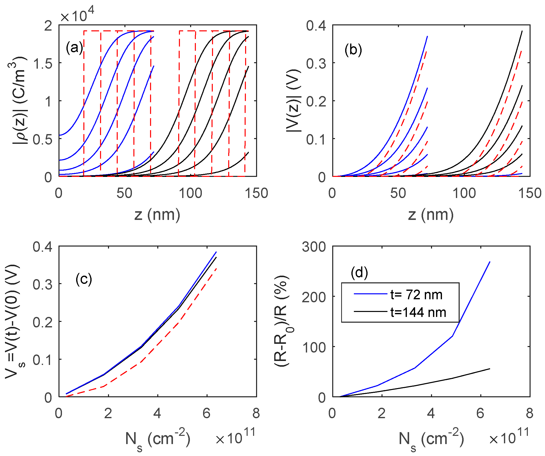
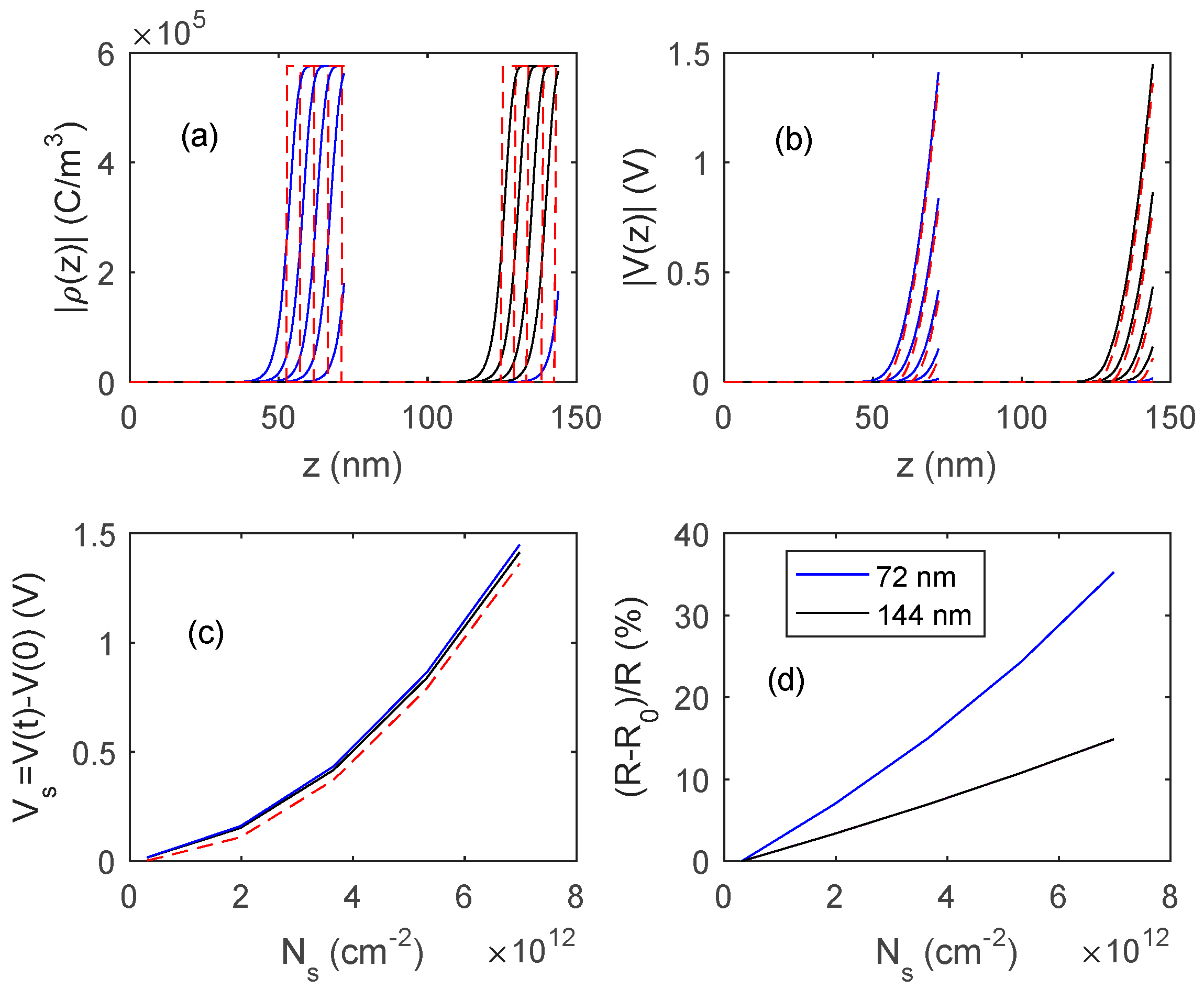
In
Figure 15 and
Figure 16, the outputs of the proposed model, obtained by numerically solving Equation (11), are shown, and compared with those obtained with fully depleted model. The presented results concern two different In
2O
3 materials, the first one (
Figure 15) is a pure material with a very low bulk carrier concentration (
Nd = 1.2 × 10
17 cm
−3) whereas the second one (
Figure 16) is characterized by a much larger
Nd value (3.6 × 10
18 cm
−3). In simulations,
Ns0 is assumed to be negligible, so the response is simply
. A comparison of the simulated results with the experimental data indicates that the obtained films behave similarly to those shown in
Figure 15, where the reduction of the film thickness from 144 nm to 72 nm provides a very large gain in terms of response, indicating that
Ndt is close to
Ns.


