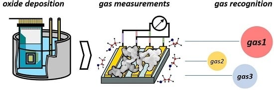
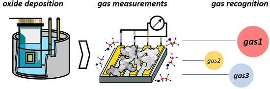
The Potentiodynamic Bottom-up Growth of the Tin Oxide Nanostructured Layer for Gas-Analytical Multisensor Array Chips

 ,
,  , ,
, ,  ,
, 
Abstract
1. Introduction
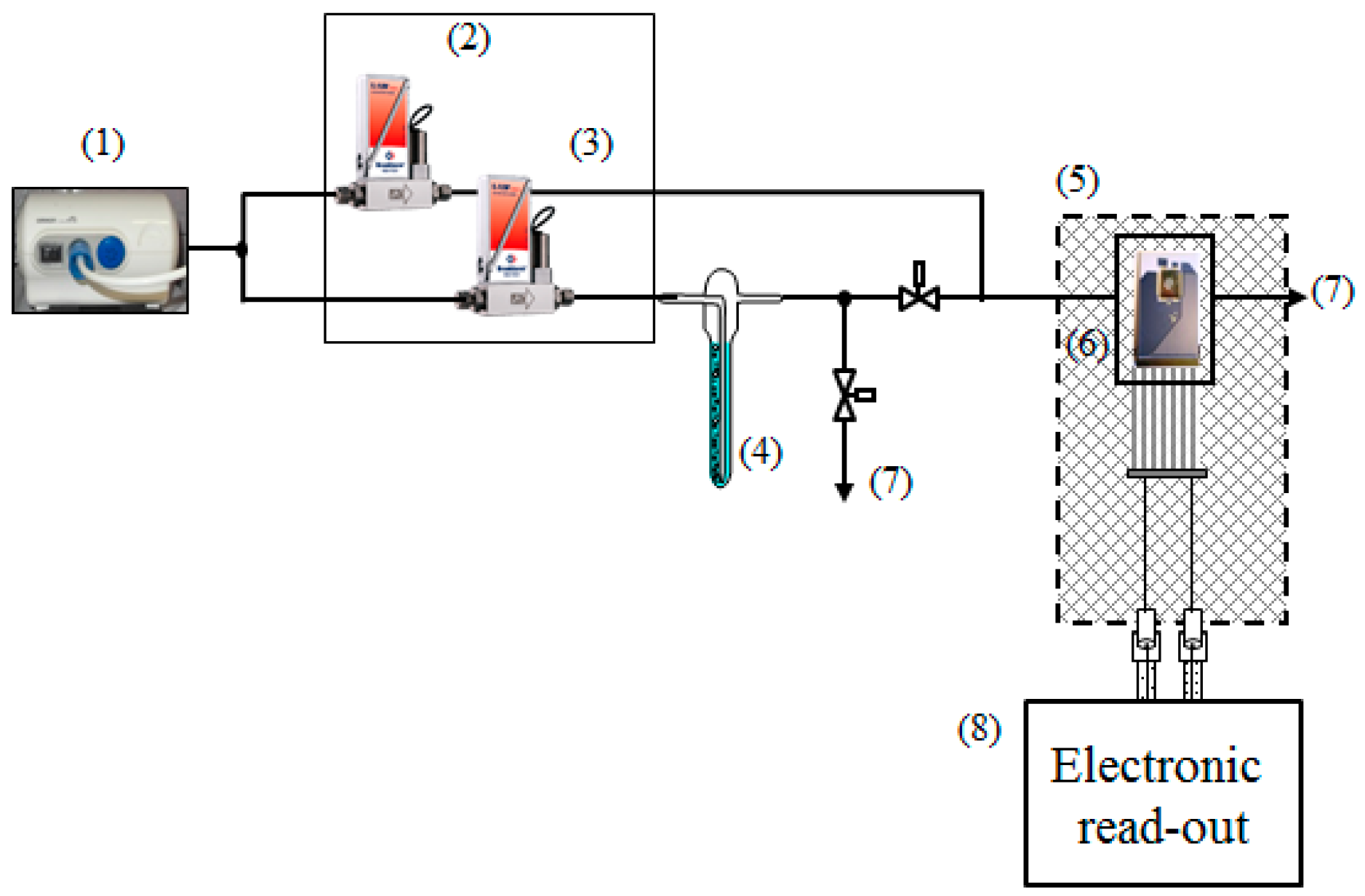
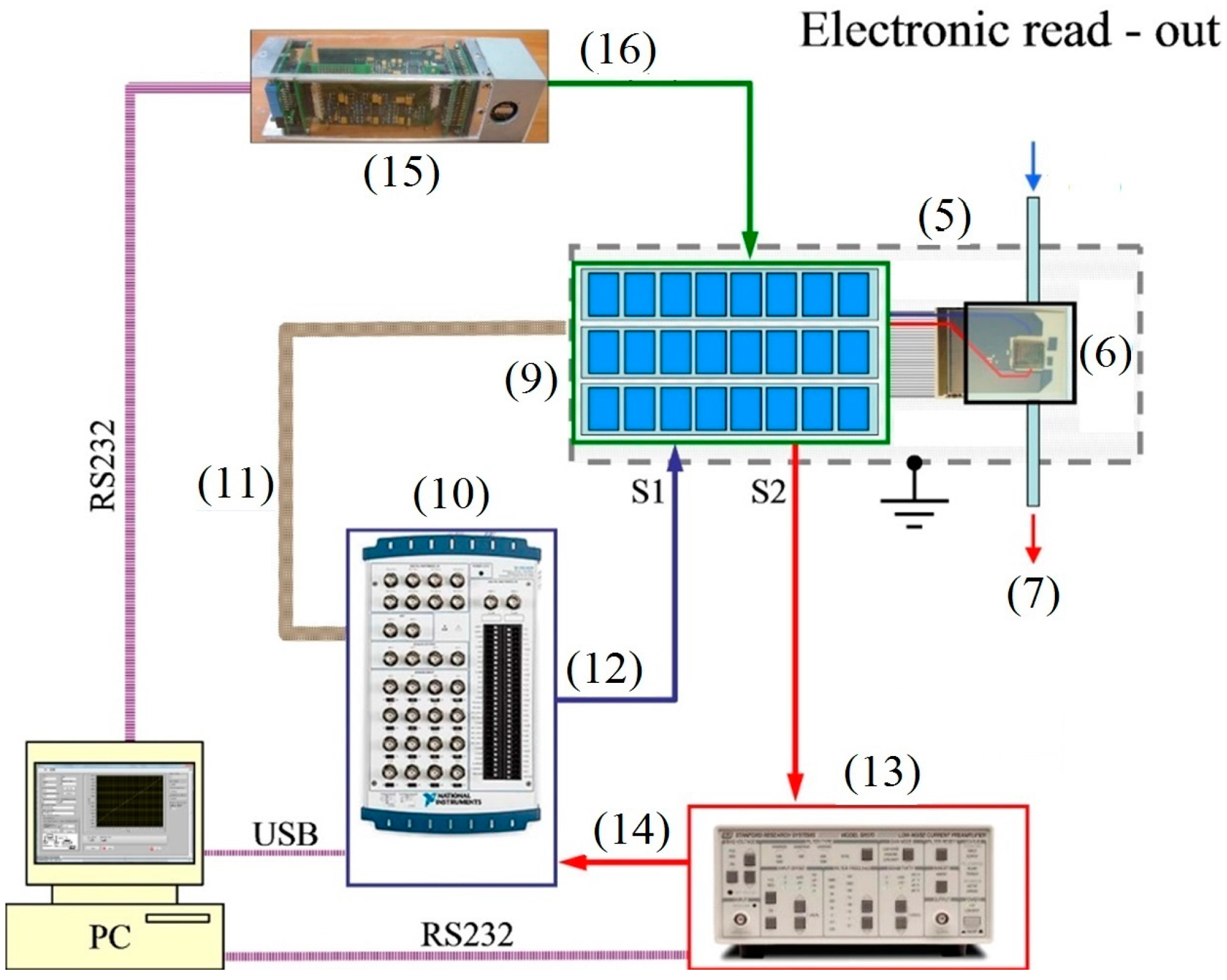
2. Experimental
3. Results and Discussion
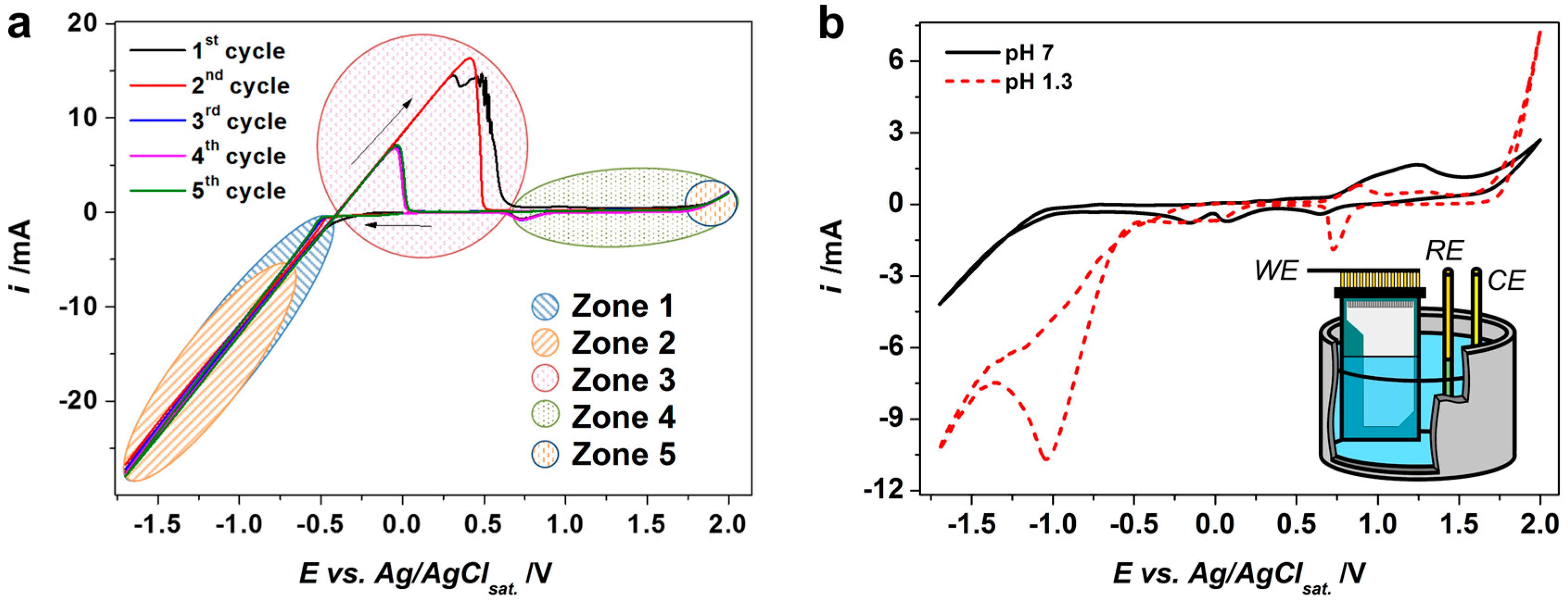
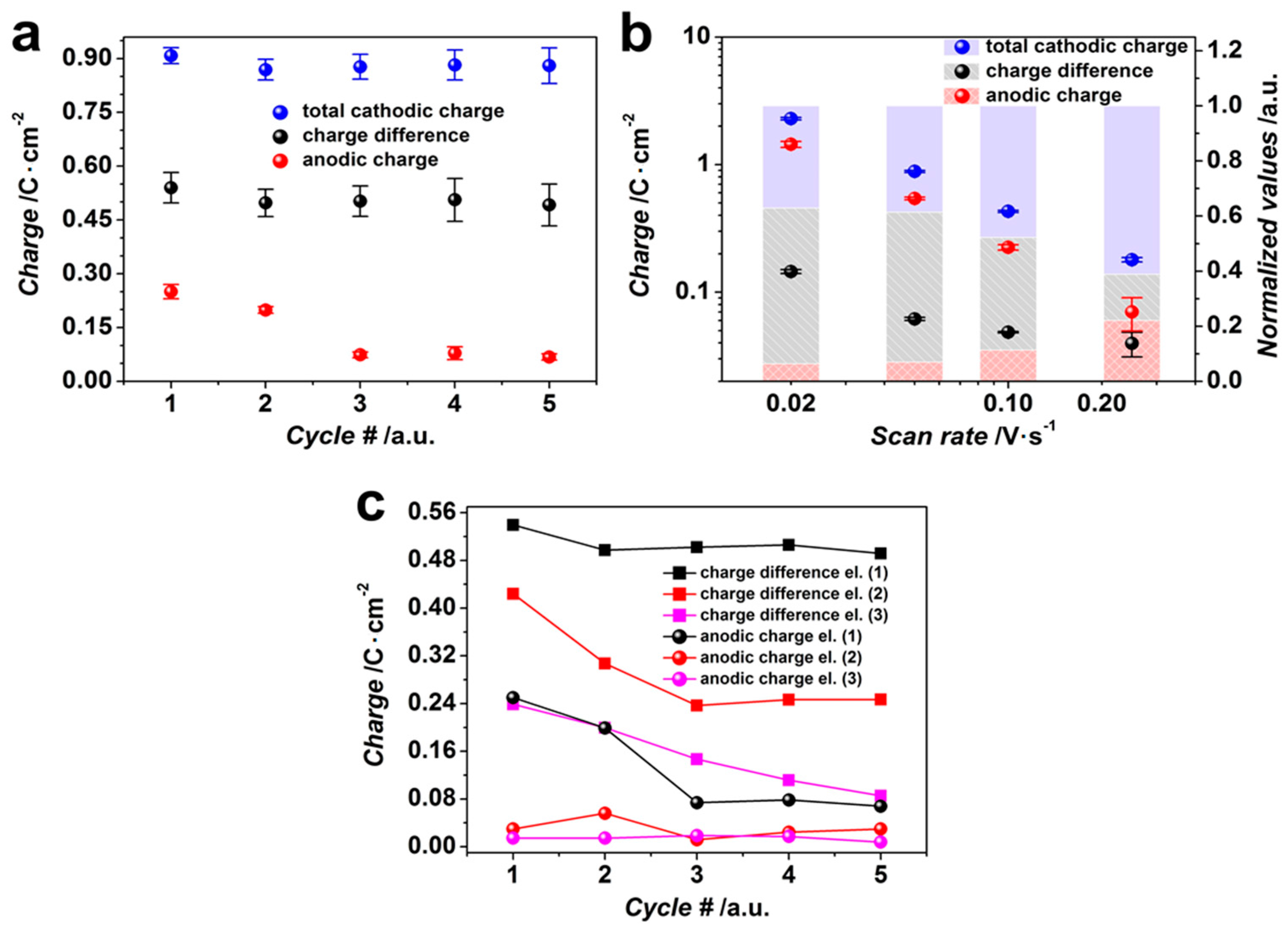
3.1. Potentiodynamic Deposition
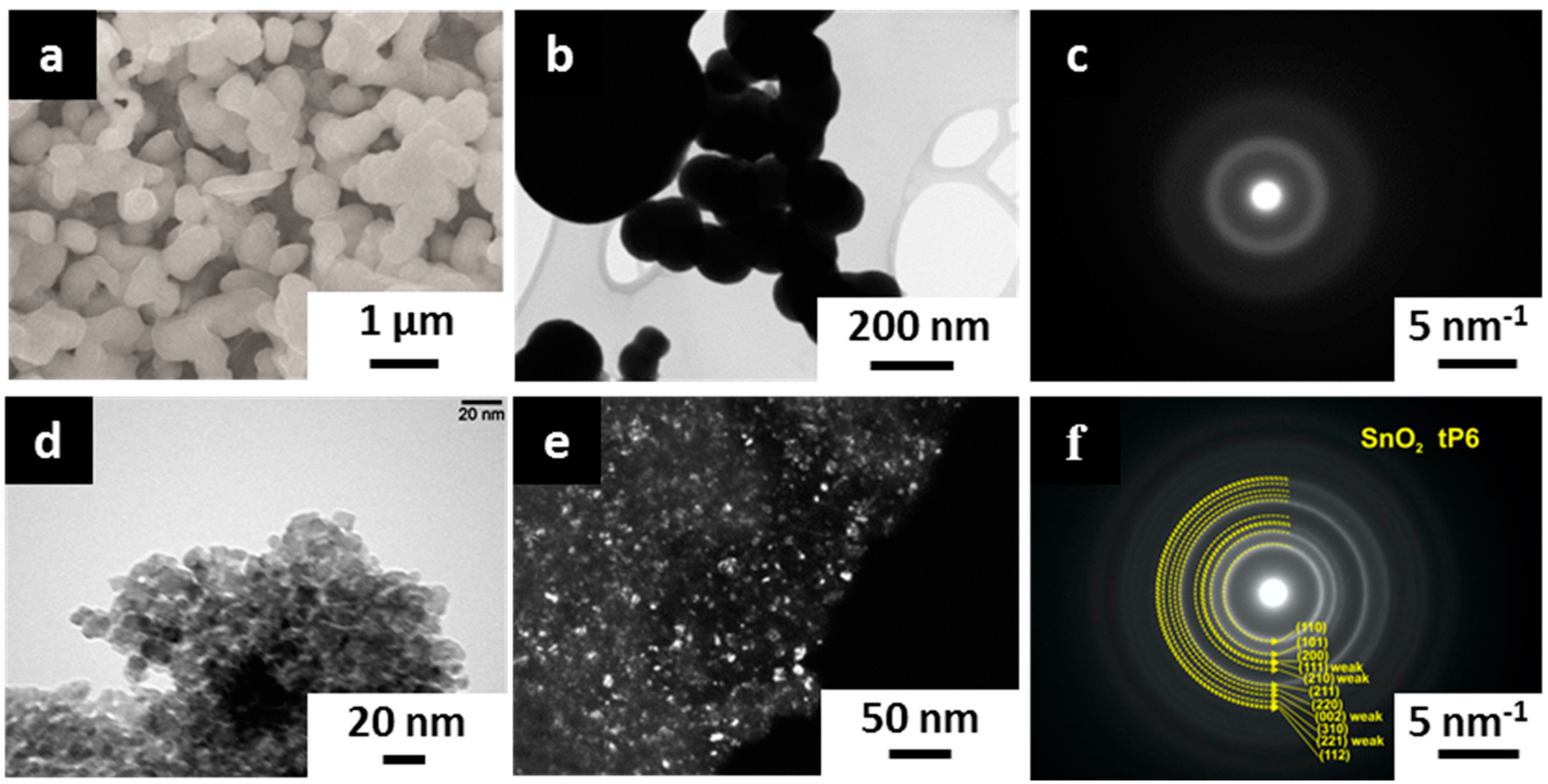
3.2. Layer Morphology and Crystal Structure
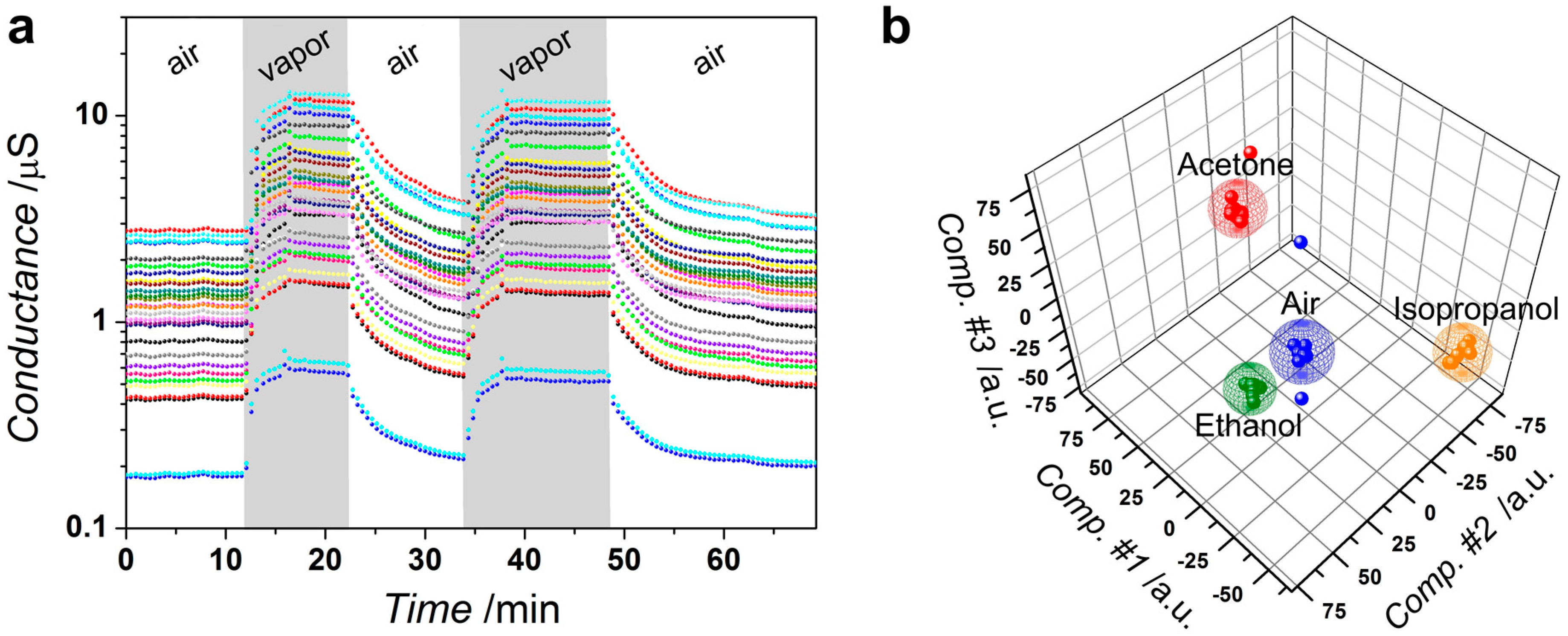
3.3. Sensor Performance
4. Conclusions
Acknowledgments
Author Contributions
Conflicts of Interest
References
- Korotcenkov, G. The role of morphology and crystallographic structure of metal oxides in response of conductometric-type gas sensors. Mater. Sci. Eng. R. Rep. 2008, 61, 1–39. [Google Scholar] [CrossRef]
- Comini, E.; Baratto, C.; Faglia, G.; Ferroni, M.; Vomiero, A.; Sberveglieri, G. Quasi-one dimensional metal oxide semiconductors: Preparation, characterization and application as chemical sensors. Prog. Mater. Sci. 2009, 54, 1–67. [Google Scholar] [CrossRef]
- Zhitomirsky, I. Cathodic electrodeposition of ceramic and organoceramic materials. Fundamental aspects. Adv. Colloid Interface Sci. 2002, 97, 279–317. [Google Scholar] [CrossRef]
- Switzer, J.A. Electrochemical synthesis of ceramic films and powders. Am. Ceram. Soc. Bull. 1987, 66, 1521–1524. [Google Scholar]
- Therese, G.H.A.; Kamath, P.V. Electrochemical synthesis of metal oxides and hydroxides. Chem. Mater. 2000, 12, 1195–1204. [Google Scholar] [CrossRef]
- Vogt, P.; Bierwagen, O. The competing oxide and sub-oxide formation in metal-oxide molecular beam epitaxy. Appl. Phys. Lett. 2015, 106, 081910. [Google Scholar] [CrossRef]
- Blanquart, T.; Niinisto, J.; Ritala, M.; Leskela, M. Atomic layer deposition of groups 4 and 5 transition metal oxide thin films: Focus on heteroleptic precursors. Chem. Vapor. Depos. 2014, 20, 189–208. [Google Scholar] [CrossRef]
- Mathur, S.; Singh, A.P.; Muller, R.; Leuning, T.; Lehnen, T.; Shen, H. Metal-organic chemical vapor deposition of metal oxide films and nanostructures. Ceram. Sci. Technol. 2013, 3–4, 291–336. [Google Scholar] [CrossRef]
- Nunes, P.; Fortunato, E.; Lopes, A.; Martins, R. Influence of the deposition conditions on the gas sensitivity of zinc oxide thin films deposited by spray pyrolysis. Int. J. Inorg. Mater. 2001, 3, 1129–1131. [Google Scholar] [CrossRef]
- Indira, L.; Kamath, P.V. Electrogeneration of base by cathodic reduction of anions: Novel one-step route to unary and layered double hydroxides (LDHs). J. Mater. Chem. 1994, 4, 1487–1490. [Google Scholar] [CrossRef]
- Brownson, J.R.S.; Lévy-Clément, C. Electrodeposition of α- and β-cobalt hydroxide thin films via dilute nitrate solution reduction. Phys. Status Solidi Basic Res. 2006, 245, 1785–1791. [Google Scholar] [CrossRef]
- Fedorov, F.S.; Linnemann, J.; Tschulik, K.; Giebeler, L.; Uhlemann, M.; Gebert, A. Capacitance performance of cobalt hydroxide-based capacitors with utilization of near-neutral electrolytes. Electrochim. Acta 2013, 90, 166–170. [Google Scholar] [CrossRef]
- Aldama, I.; Barranco, V.; Centeno, T.A.; Ibañez, J.; Rojo, J.M. Composite electrodes made from carbon cloth as supercapacitor material and manganese and cobalt oxide as battery one. J. Electrochem. Soc. 2016, 163, A758–A765. [Google Scholar] [CrossRef][Green Version]
- Murthy, M.; Nagarajan, G.S.; Weidner, J.W.; Van Zee, J.W. A model for the galvanostatic deposition of nickel hydroxide. J. Electrochem. Soc. 1996, 143, 2319–2327. [Google Scholar] [CrossRef][Green Version]
- Jayashree, R.S.; Kamath, P.V. Nickel hydroxide electrodeposition from nickel nitrate solutions: Mechanistic studies. J. Power Sources 2001, 93, 273–278. [Google Scholar] [CrossRef]
- Izaki, M.; Omi, T. Transparent zinc oxide films prepared by electrochemical reaction. Appl. Phys. Lett. 1996, 68, 2439–2440. [Google Scholar] [CrossRef]
- Izaki, M.; Omi, T. Electrolyte optimization for cathodic growth of zinc oxide films. J. Electrochem. Soc. 1996, 143, L53–L55. [Google Scholar] [CrossRef]
- Peulon, S.; Lincot, D. Cathodic electrodeposition from aqueous solution of dense or open-structured zinc oxide films. Adv. Mater. 1996, 8, 166–170. [Google Scholar] [CrossRef]
- Bard, A.J.; Parsons, R.; Jordan, J. Standard Potentials in Aqueous Solutions; Marcel Dekker: New York, NY, USA, 1985. [Google Scholar]
- Chen, X.; Liang, J.; Zhou, Z.; Duan, H.; Li, B.; Yang, Q. The preparation of SnO2 film by electrodeposition. Mater. Res. Bull. 2010, 45, 2006–2011. [Google Scholar] [CrossRef]
- Chang, S.T.; Leu, I.C.; Hon, M.H. Preparation and characterization of nanostructured tin oxide films by electrochemical deposition. Electrochem. Solid-State Lett. 2002, 5, C71–C74. [Google Scholar] [CrossRef]
- Hu, J.; Zhu, Y.-F.; Liu, Q.; Gao, Y.-B.; Du, R.-G.; Lin, C.-J. SnO2 nanoparticle films prepared by pulse current deposition for photocathodic protection of stainless steel. J. Electrochem. Soc. 2015, 162, C161–C166. [Google Scholar] [CrossRef]
- Lai, M.; Lim, J.-H.; Mubeen, S.; Rheem, Y.; Mulchandani, A.; Deshusses, M.A.; Myung, N.V. Size-controlled electrochemical synthesis and properties of SnO2 nanotubes. Nanotechnology 2009, 20, 185602. [Google Scholar] [CrossRef] [PubMed]
- Mubeen, S.; Lai, M.; Zhang, T.; Lim, J.-H.; Mulchandani, A.; Deshusses, M.A.; Myung, N.V. Hybrid tin oxide-SWNT nanostructures based gas sensor. Electrochim. Acta 2013, 92, 484–490. [Google Scholar] [CrossRef]
- Spray, R.L.; Choi, K.-S. Electrochemical synthesis of SnO2 films containing three-dimensionally organized uniform mesopores via interfacial surfactant templating. Chem. Commun. 2007, 35, 3655–3657. [Google Scholar] [CrossRef] [PubMed]
- Kuriganova, A.B.; Smirnova, N.V. Pt/SnOx-C composite material for electrocatalysis. Mendeleev Commun. 2014, 24, 351–352. [Google Scholar] [CrossRef]
- Goschnick, J. An electronic nose for intelligent consumer products based on a gas analytical gradient microarray. Microelectron. Eng. 2001, 57–58, 693–704. [Google Scholar] [CrossRef]
- Sysoev, V.V.; Kiselev, I.; Frietsch, M.; Goschnick, J. Temperature gradient effect on gas discrimination power of a metal-oxide thin-film sensor microarray. Sensors 2004, 4, 37–46. [Google Scholar] [CrossRef]
- Saturated Vapor Pressure. Available online: http://ddbonline.ddbst.de/AntoineCalculation/AntoineCalculationCGI.exe (accessed on 20 July 2017).
- Hierlemann, A.; Gutierrez-Osuna, R. Higher-order chemical sensing. Chem. Rev. 2008, 108, 563–613. [Google Scholar] [CrossRef] [PubMed]
- Mishra, S.; Lawrence, F.; Mallika, C.; Pandey, N.K.; Srinivasan, R.; Mudali, U.K.; Natarajan, R. Kinetics of reduction of nitric acid by electrochemical method and validation of cell design for plant application. Electrochim. Acta 2015, 160, 219–226. [Google Scholar] [CrossRef]
- De, D.; Kalu, E.E.; Tarjan, P.P.; Englehardt, J.D. Kinetic studies of the electrochemical treatment of nitrate and nitrite ions on iridium-modified carbon fiber electrodes. Chem. Eng. Technol. 2004, 27, 56–64. [Google Scholar] [CrossRef]
- Petrii, O.A.; Safonova, T.Y. Electroreduction of nitrate and nitrite anions on platinum metals: A model process for elucidating the nature of the passivation by hydrogen adsorption. J. Electroanal. Chem. 1992, 331, 897–912. [Google Scholar] [CrossRef]
- Polatides, C.; Kyriacou, G. Electrochemical reduction of nitrate ion on various cathodes - reaction kinetics on bronze cathode. J. Appl. Electrochem. 2005, 35, 421–427. [Google Scholar] [CrossRef]
- Dogonadze, R.R.; Ulstrup, J.; Kharkats, Y.I. A theory of electrode reactions through bridge transition states; bridges with a discrete electronic spectrum. J. Electroanal. Chem. 1972, 39, 47–61. [Google Scholar] [CrossRef]
- Nazmutdinov, R.R.; Glukhov, D.V.; Tsirlina, G.A.; Petrii, O.A. Molecular description of the persulfate ion reduction on a mercury electrode. Russ. J. Electrochem. 2002, 38, 720–731. [Google Scholar] [CrossRef]
- Katsounaros, I.; Kyriacou, G. Influence of the concentration and the nature of the supporting electrolyte on the electrochemical reduction of nitrate on tin cathode. Electrochim. Acta 2007, 52, 6412–6420. [Google Scholar] [CrossRef]
- Xu, C.; Tamaki, J.; Miura, N.; Yamazoe, N. Grain size effects on gas sensitivity of porous SnO2-based elements. Sens. Actuators B 1991, 3, 147–155. [Google Scholar] [CrossRef]
- Bender, M.; Fortunato, E.; Nunes, P.; Ferreira, I.; Marques, A.; Martins, R.; Katsarakis, N.; Cimalla, V.; Kiriakidis, G. Highly sensitive ZnO ozone detectors at room temperature. Jpn. J. Appl. Phys. 2003, 42, L435–L437. [Google Scholar] [CrossRef]
- Barsan, N.; Weimar, U. Understanding the fundamental principles of metal oxide based gas sensors; the example of CO sensing with SnO2 sensors in the presence of humidity. J. Phys. Condens. Matter. 2003, 15, R813–R839. [Google Scholar] [CrossRef]
- Korotchenkov, G.; Sysoev, V.V. Conductometric metal oxide gas sensors: Principles of operation and technological approaches to fabrication. In Chemical Sensors: Comprehensive Sensor Technologies, Vol. 4: Solid State Sensors; Korotchenkov, G., Ed.; Momentum Press: New York, NY, USA, 2011; Volume 4, pp. 53–186. ISBN 978-1-60650-233-4. [Google Scholar]
- Windischmann, H.; Mark, P. A model for the operation of a thin-film SnOx conductance-modulation carbon monoxide sensor. J. Electrochem. Soc. 1979, 126, 627–633. [Google Scholar] [CrossRef]
- Sysoev, V.V.; Goschnick, J.; Schneider, T.; Strelcov, E.; Kolmakov, A. A gradient microarray electronic nose based on percolating SnO2 nanowire sensing elements. Nano Lett. 2007, 7, 3182–3188. [Google Scholar] [CrossRef] [PubMed]
- Wolkenstein, T.B. Electronic Processes on Semiconductor Surfaces during Chemisorption; Consultants Bureau: New York, NY, USA, 1991. [Google Scholar]
- Persaud, K.; Dodd, G. Analysis of discrimination mechanisms in the mammalian olfactory system using a model nose. Nature 1982, 299, 352–355. [Google Scholar] [CrossRef] [PubMed]
- Ellis, J.E.; Star, A. Carbon nanotube based gas sensors toward breath analysis. Chempluschem 2016, 81, 1248–1265. [Google Scholar] [CrossRef]


© 2017 by the authors. Licensee MDPI, Basel, Switzerland. This article is an open access article distributed under the terms and conditions of the Creative Commons Attribution (CC BY) license (http://creativecommons.org/licenses/by/4.0/).
Share and Cite
Fedorov, F.S.; Podgainov, D.; Varezhnikov, A.; Lashkov, A.; Gorshenkov, M.; Burmistrov, I.; Sommer, M.; Sysoev, V. The Potentiodynamic Bottom-up Growth of the Tin Oxide Nanostructured Layer for Gas-Analytical Multisensor Array Chips. Sensors 2017, 17, 1908. https://doi.org/10.3390/s17081908
Fedorov FS, Podgainov D, Varezhnikov A, Lashkov A, Gorshenkov M, Burmistrov I, Sommer M, Sysoev V. The Potentiodynamic Bottom-up Growth of the Tin Oxide Nanostructured Layer for Gas-Analytical Multisensor Array Chips. Sensors. 2017; 17(8):1908. https://doi.org/10.3390/s17081908
Chicago/Turabian StyleFedorov, Fedor S., Dmitry Podgainov, Alexey Varezhnikov, Andrey Lashkov, Michail Gorshenkov, Igor Burmistrov, Martin Sommer, and Victor Sysoev. 2017. "The Potentiodynamic Bottom-up Growth of the Tin Oxide Nanostructured Layer for Gas-Analytical Multisensor Array Chips" Sensors 17, no. 8: 1908. https://doi.org/10.3390/s17081908
APA StyleFedorov, F. S., Podgainov, D., Varezhnikov, A., Lashkov, A., Gorshenkov, M., Burmistrov, I., Sommer, M., & Sysoev, V. (2017). The Potentiodynamic Bottom-up Growth of the Tin Oxide Nanostructured Layer for Gas-Analytical Multisensor Array Chips. Sensors, 17(8), 1908. https://doi.org/10.3390/s17081908