Review of Recent Inkjet-Printed Capacitive Tactile Sensors


Abstract
:1. Introduction
- (1)
- Stable and hysteresis-free behavior
- (2)
- Monotonic response (better if linear)
- (3)
- Conformable interface, robust and inexpensive
2. Inkjet-Printing Technology
2.1. Inkjet Printing
2.2. Substrate Materials
2.3. Conductive Inks and Sintering
2.4. Resolution of Inkjet Printing
2.5. Challenges and Strategies of Inkjet Printing
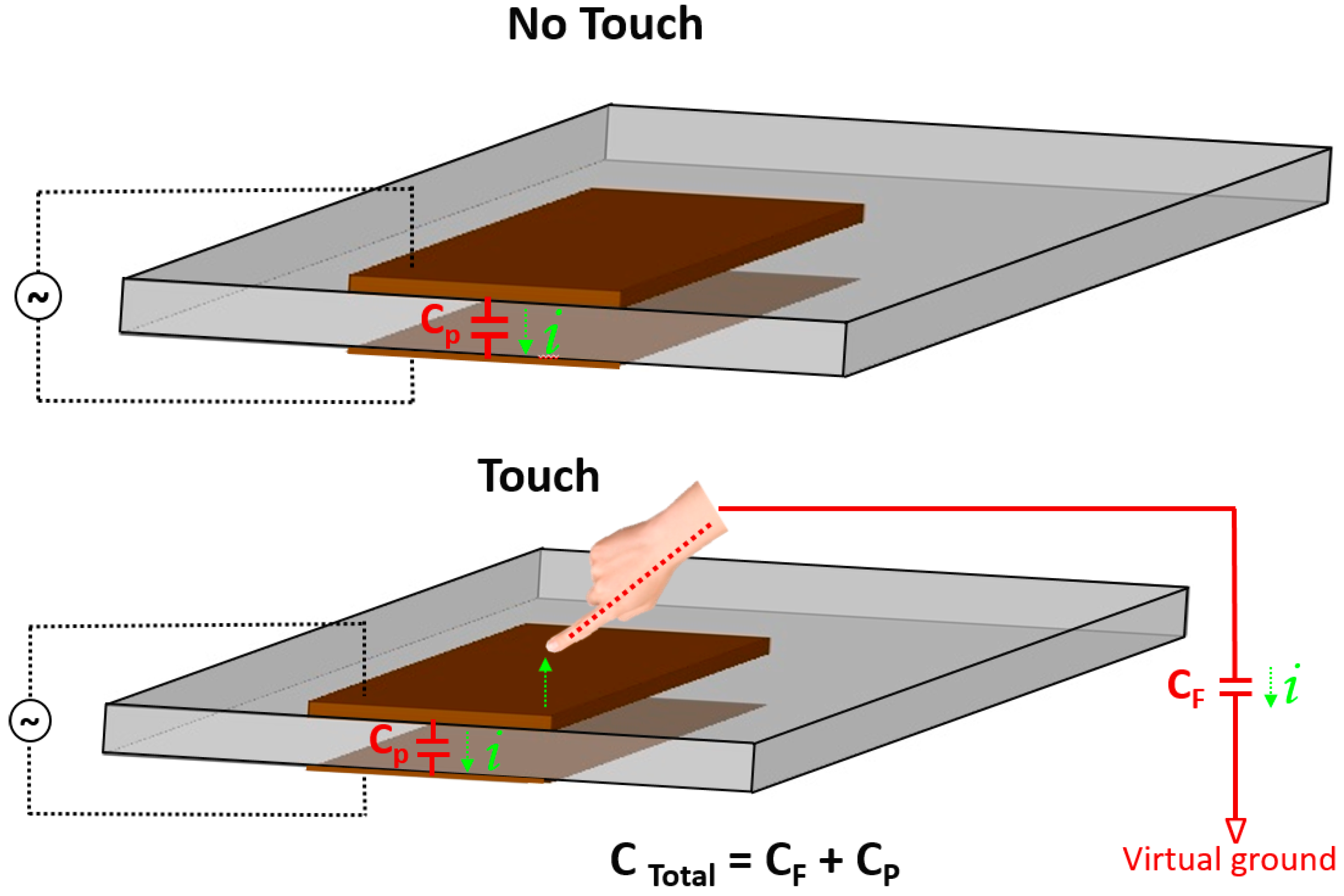
3. Capacitive Tactile Sensors
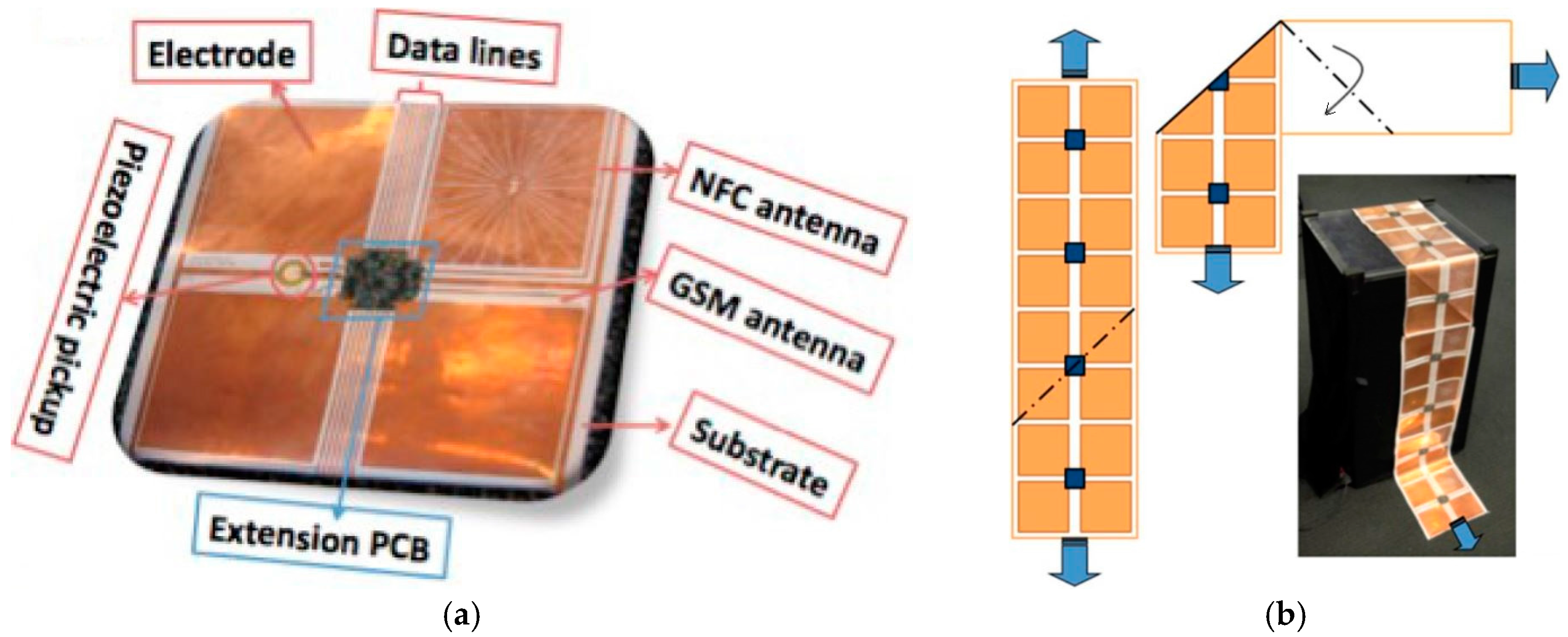
3.1. Inkjet-Printed Tactile Sensors on Flexible Substrates
3.1.1. Inkjet-Printed Tactile Sensors on Polymer Substrates
3.1.2. Inkjet-Printed Tactile Sensors on Paper Substrates
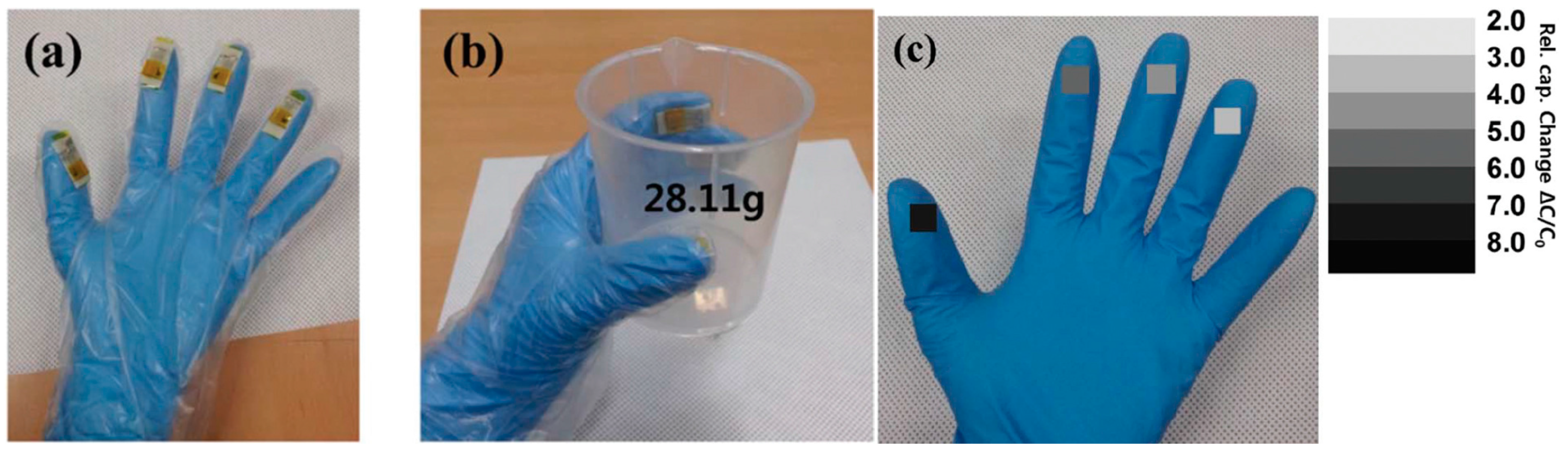
3.1.3. Inkjet-Printed Tactile Sensors on Textile Substrate
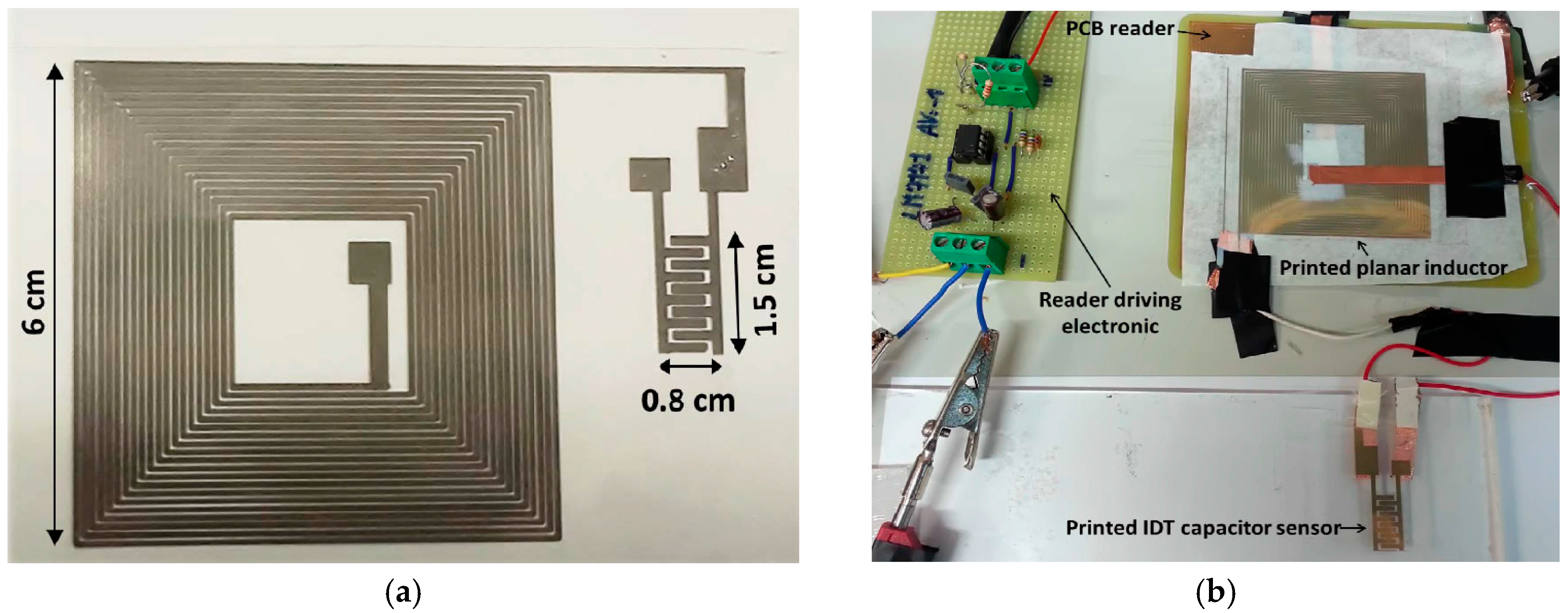
3.2. Inkjet-Printed Tactile Sensors on Rigid Substrates
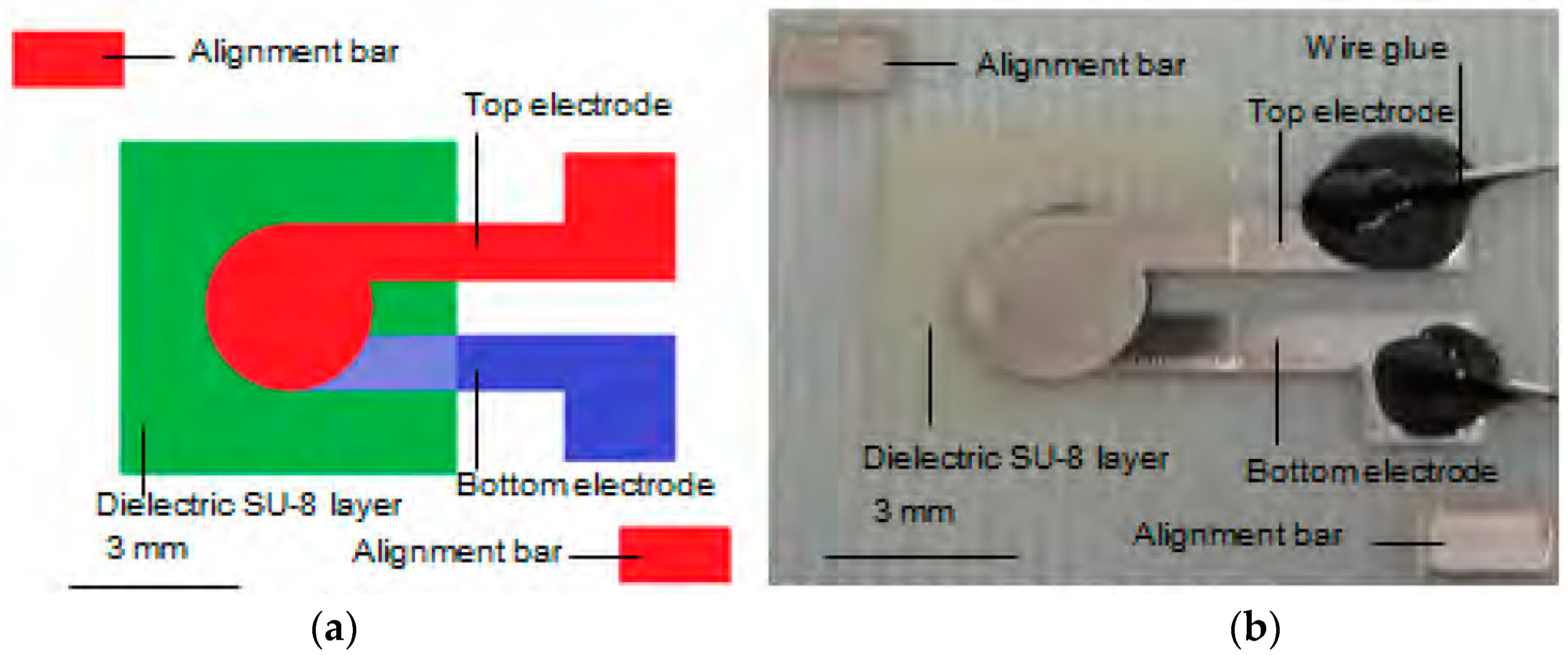
Inkjet-Printed Tactile Sensors on Glass Substrates
4. Conclusions
Acknowledgments
Author Contributions
Conflicts of Interest
References
- Walker, G. Touch Technologies Tutorial Latest Version by Intel. 2014. Available online: http://www.walkermobile.com/TGM_2014_Touch_Technologies_Tutorial.pdf (accessed on 10 November 2017).
- Dahiya, R.S.; Metta, G.; Valle, M.; Sandini, G. Tactile Sensing—From Humans to Humanoids. IEEE Trans. Robot. 2010, 26, 1–20. [Google Scholar] [CrossRef]
- Chiolerio, A.; Rivolo, P.; Porro, S.; Stassi, S.; Ricciardi, S.; Mandracci, P.; Canavese, G.; Bejtka, K.; Pirri, C.F. Inkjet-printed PEDOT:PSS electrodes on plasma-modified PDMS nanocomposites: Quantifying plasma treatment hardness. RSC Adv. 2014, 4, 51477–51485. [Google Scholar] [CrossRef]
- Harmon, L.D. Automated Tactile Sensing. Int. J. Rob. Res. 1982, 1, 3–32. [Google Scholar] [CrossRef]
- Saad, R.E.; Bonen, A.; Smith, K.C.; Benhabib, B. Tactile Sensing_Ch 25. In Measurement, Instrumentation and Sensors Handbook; Webster, J.G., Halit, E., Eds.; Crc Press Llc: Boca Raton, FL, USA, 1999; ISBN 978-0-8493-8347-2. [Google Scholar]
- Bartolozzi, C.; Natale, L.; Nori, F.; Metta, G. Robots with a sense of touch. Nat. Mater. 2016, 15, 921–925. [Google Scholar] [CrossRef] [PubMed]
- Qin, H.; Dong, J.; Lee, Y.S. Fabrication and electrical characterization of multi-layer capacitive touch sensors on flexible substrates by additive e-jet printing. J. Manuf. Process. 2016, 28, 479–485. [Google Scholar] [CrossRef]
- Rocha, J.G.; Lanceros-Mendez, S. Sensors, Focus on Tactile, Force and Stress Sensors; INTECH: Rijeka, Croatia, 2008; ISBN 978-953-7619-31-2. [Google Scholar]
- Lakafosis, V.; Rida, A.; Vyas, R.; Yang, L.; Nikolaou, S.; Tentzeris, M.M. Progress towards the first wireless sensor networks consisting of inkjet-printed, paper-based RFID-enabled sensor tags. Proc. IEEE 2010, 98, 1601–1609. [Google Scholar] [CrossRef]
- Son, S.; Park, J.E.; Lee, J.; Yang, M.; Kang, B. Laser-assisted fabrication of single-layer flexible touch sensor. Sci. Rep. 2016, 6, 34629. [Google Scholar] [CrossRef] [PubMed]
- Aleksandrova, M.; Kolev, G.; Cholakova, I.; Dobrikov, G.; Bodurov, G. Photolithography versus lift off process for patterning of sputtered. Int. J. Thin Film. Sci. Technol. 2013, 2, 67–75. [Google Scholar] [CrossRef]
- Liao, W.C.; Hsu, S.L.C.; Chu, S.Y.; Kau, P.C. Imprint lithography for flexible transparent plastic substrates. Microelectron. Eng. 2004, 75, 145–148. [Google Scholar] [CrossRef]
- Simon, D.; Ware, T.; Marcotte, R.; Lund, B.R.; Smith, D.W.; Di Prima, M.; Rennaker, R.L.; Voit, W. A comparison of polymer substrates for photolithographic processing of flexible bioelectronics. Biomed. Microdevices 2013, 15, 925–939. [Google Scholar] [CrossRef] [PubMed]
- Yin, Z.P.; Huang, Y.A.; Bu, N.B.; Wang, X.M.; Xiong, Y.L. Inkjet printing for flexible electronics: Materials, processes and equipments. Chin. Sci. Bull. 2010, 55, 3383–3407. [Google Scholar] [CrossRef]
- Sele, C.W.; Von Werne, T.; Friend, R.H.; Sirringhaus, H. Lithography-free, self-aligned inkjet printing with sub-hundred-nanometer resolution. Adv. Mater. 2005, 17, 997–1001. [Google Scholar] [CrossRef]
- Hon, K.K. B.; Li, L.; Hutchings, I.M. Direct writing technology-Advances and developments. CIRP Ann. Manuf. Technol. 2008, 57, 601–620. [Google Scholar] [CrossRef]
- Andò, B.; Baglio, S.; Bulsara, A.R.; Emery, T.; Marletta, V.; Pistorio, A. Low-cost inkjet printing technology for the rapid prototyping of transducers. Sensors 2017, 17, 748. [Google Scholar] [CrossRef] [PubMed]
- Yang, L.; Rida, A.; Vyas, R.; Tentzeris, M.M. RFID tag and RF structures on a paper substrate using inkjet-printing technology. IEEE Trans. Microw. Theory Tech. 2007, 55, 2894–2901. [Google Scholar] [CrossRef]
- Ling, K.; Yoo, M.; Su, W.; Kim, K.; Cook, B.; Tentzeris, M.M.; Lim, S. Microfluidic tunable inkjet-printed metamaterial absorber on paper. Opt. Express 2015, 23, 110. [Google Scholar] [CrossRef] [PubMed]
- Lessing, J.; Glavan, A.C.; Walker, S.B.; Keplinger, C.; Lewis, J.A.; Whitesides, G.M. Inkjet printing of conductive inks with high lateral resolution on omniphobic “RF paper” for paper-based electronics and MEMS. Adv. Mater. 2014, 26, 4677–4682. [Google Scholar] [CrossRef] [PubMed]
- Nery, E.W.; Kubota, L.T. Sensing approaches on paper-based devices: A review. Anal. Bioanal. Chem. 2013, 405, 7573–7595. [Google Scholar] [CrossRef] [PubMed]
- Wang, Y.; Guo, H.; Chen, J.J.; Sowade, E.; Wang, Y.; Liang, K.; Marcus, K.; Baumann, R.R.; Feng, Z.S. Paper-Based Inkjet-Printed Flexible Electronic Circuits. ACS Appl. Mater. Interfaces 2016, 8, 26112–26118. [Google Scholar] [CrossRef] [PubMed]
- Eom, S.; Lim, S. Stretchable complementary split ring resonator (CSRR)-based radio frequency (RF) sensor for strain direction and level detection. Sensors 2016, 16, 1667. [Google Scholar] [CrossRef] [PubMed]
- Khan, S.; Lorenzelli, L.; Dahiya, R.S. Technologies for printing sensors and electronics over large flexible substrates: A review. IEEE Sens. J. 2015, 15, 3164–3185. [Google Scholar] [CrossRef]
- Li, Y.; Torah, R.; Beeby, S.; Tudor, J. An all-inkjet printed flexible capacitor on a textile using a new poly(4-vinylphenol) dielectric ink for wearable applications. Proc. IEEE Sens. 2012, 5–8. [Google Scholar] [CrossRef]
- Gao, M.; Li, L.; Song, Y. Inkjet printing wearable electronic devices. J. Mater. Chem. C 2017, 5, 2971–2993. [Google Scholar] [CrossRef]
- Nguyen, T.M.; Chung, J. RF Conductivity Measurement of Conductive Zell Fabric. J. Electromagn. Eng. Sci. 2016, 16, 24–28. [Google Scholar] [CrossRef]
- Salvado, R.; Loss, C.; Gonçalves, R.; Pinho, P. Textile materials for the design of wearable antennas: A survey. Sensors 2012, 12, 15841–15857. [Google Scholar] [CrossRef] [PubMed]
- Memon, M.U.; Tentzeris, M.M.; Lim, S. Inkjet-printed 3D Hilbert-curve fractal antennas for VHF band. Microw. Opt. Technol. Lett. 2017, 59, 1698–1704. [Google Scholar] [CrossRef]
- Salim, A.; Lim, S. Complementary Split-Ring Resonator-Loaded Microfluidic Ethanol Chemical Sensor. Sensors 2016, 16, 1802. [Google Scholar] [CrossRef] [PubMed]
- Lee, D.; Sung, H.K.; Lim, S. Flexible subterahertz metamaterial absorber fabrication using inkjet printing technology. Appl. Phys. B 2016, 122, 1–8. [Google Scholar] [CrossRef]
- Stoppa, M.; Chiolerio, A. Wearable electronics and smart textiles: A critical review. Sensors 2014, 14, 11957–11992. [Google Scholar] [CrossRef] [PubMed]
- Chen, S.-P.; Chiu, H.-L.; Wang, P.-H.; Liao, Y.-C. Inkjet Printed Conductive Tracks for Printed Electronics. ECS J. Solid State Sci. Technol. 2015, 4, P3026–P3033. [Google Scholar] [CrossRef]
- Wünscher, S.; Abbel, R.; Perelaer, J.; Schubert, U.S. Progress of alternative sintering approaches of inkjet-printed metal inks and their application for manufacturing of flexible electronic devices. J. Mater. Chem. C 2014, 2, 10232–10261. [Google Scholar] [CrossRef]
- Fang, Y.; Akbari, M.; Sydänheimo, L.; Ukkonen, L.; Tentzeris, M.M. Sensitivity enhancement of flexible gas sensors via conversion of inkjet-printed silver electrodes into porous gold counterparts. Sci. Rep. 2017, 7, 8988. [Google Scholar] [CrossRef] [PubMed]
- Lee, J.; Lee, B. Design of Thin RC Absorbers Using a Silver Nanowire Resistive Screen. J. Elecromagn. Eng. Sci. 2016, 16, 106–111. [Google Scholar] [CrossRef]
- Gaspar, C.; Olkkonen, J.; Passoja, S.; Smolander, M. Paper as active layer in inkjet-printed capacitive humidity sensors. Sensors 2017, 17, 1464. [Google Scholar] [CrossRef]
- Andò, B.; Baglio, S.; Marletta, V.; Pistorio, A. A contactless inkjet printed passive touch sensor. In Proceedings of the 2014 IEEE International Instrumentation and Measurement Technology Conference (I2MTC), Montevideo, Uruguay, 12–15 May 2014. [Google Scholar] [CrossRef]
- Kim, H.K.; Lee, D.; Lim, S. A fluidically tunable metasurface absorber for flexible large-scale wireless ethanol sensor applications. Sensors 2016, 16, 1246. [Google Scholar] [CrossRef] [PubMed]
- DuPont: Strecthable Inks for Wearable Electronics. Available online: http://www.dupont.com/products-and-services/electronic-electrical-materials/printed-electronics/products/stetchable-inks-for-wearable-electronics.html (accessed on 6 August 2017).
- Du, H.; Wan, T.; Qu, B.; Cao, F.; Lin, Q.; Chen, N.; Lin, X.; Chu, D. Engineering Silver Nanowire Networks: From Transparent Electrodes to Resistive Switching Devices. ACS Appl. Mater. Interfaces 2017, 9, 20762–20770. [Google Scholar] [CrossRef] [PubMed]
- Ma, S.; Ribeiro, F.; Powell, K.; Lutian, J.; Møller, C.; Large, T.; Holbery, J. Fabrication of Novel Transparent Touch Sensing Device via Drop-on-Demand Inkjet Printing Technique. ACS Appl. Mater. Interfaces 2015, 7, 21628–21633. [Google Scholar] [CrossRef] [PubMed]
- Hwang, M.S.; Jeong, B.Y.; Moon, J.; Chun, S.K.; Kim, J. Inkjet-printing of indium tin oxide (ITO) films for transparent conducting electrodes. Mater. Sci. Eng. B 2011, 176, 1128–1131. [Google Scholar] [CrossRef]
- Li, Y.; Torah, R.; Beeby, S.; Tudor, J. An all-inkjet printed flexible capacitor for wearable applications. In Proceedings of the 2012 IEEE SENSORS, Taipei, Taiwan, 28–31 October 2012. [Google Scholar] [CrossRef]
- Singh, M.; Haverinen, H.M.; Dhagat, P.; Jabbour, G.E. Inkjet printing-process and its applications. Adv. Mater. 2010, 22, 673–685. [Google Scholar] [CrossRef] [PubMed]
- Kamyshny, A.; Magdassi, S. Conductive nanomaterials for printed electronics. Small 2014, 10, 3515–3535. [Google Scholar] [CrossRef] [PubMed]
- Grubb, P.M.; Subbaraman, H.; Park, S.; Akinwande, D.; Chen, R.T. Inkjet Printing of High Performance Transistors with Micron Order Chemically Set Gaps. Sci. Rep. 2017, 7, 1202. [Google Scholar] [CrossRef] [PubMed]
- Dimatix Materials Printer DMP-2831. Available online: http://www.fujifilmusa.com/products/industrial_inkjet_printheads/deposition-products (accessed on 8 August 2017).
- Kim, S.-Y.; Kim, K.; Hwang, Y.H.; Park, J.; Jang, J.; Nam, Y.; Kang, Y.; Kim, M.; Park, H.J.; Lee, Z.; et al. High-resolution electro hydrodynamic inkjet printing of stretchable metal oxide semiconductor transistors with high performance. Nanoscale 2016, 8, 17113–17121. [Google Scholar] [CrossRef] [PubMed]
- Kwon, H.J.; Chung, S.; Jang, J.; Grigoropoulos, C.P. Laser direct writing and inkjet printing for a sub-2 μm channel length MoS2 transistor with high-resolution electrodes. Nanotechnology 2016, 27. [Google Scholar] [CrossRef] [PubMed]
- Zhang, Z.; Zhang, X.; Xin, Z.; Deng, M.; Wen, Y.; Song, Y. Synthesis of monodisperse silver nanoparticles for ink-jet printed flexible electronics. Nanotechnology 2011, 22, 425601. [Google Scholar] [CrossRef] [PubMed]
- Lau, G.-K.; Shrestha, M. Ink-Jet Printing of Micro-Electro-Mechanical Systems (MEMS). Micromachines 2017, 8, 194. [Google Scholar] [CrossRef]
- Clogged Nozzles. Available online: http://www.inkmagic.com/shopcontent.asp?type=Unclog_Epson_Printhead_Nozzles (accessed on 8 August 2017).
- How to Clean Printer Heads? Available online: http://www.castleink.com/category/82/Cleaning-Clogged-Canon-Print-Heads.html (accessed on 8 August 2017).
- Ma, S.; Liu, L.; Bromberg, V.; Singler, T.J. Fabrication of highly electrically conducting fine patterns via substrate-independent inkjet printing of mussel-inspired organic nano-material. J. Mater. Chem. C 2014, 2, 3885–3889. [Google Scholar] [CrossRef]
- Sridhar, A.; Reiding, J.; Adelaar, H.; Achterhoek, F.; van Dijk, D.J.; Akkerman, R. Inkjet-printing- and electroless-plating- based fabrication of RF circuit structures on high-frequency substrates. J. Micromech. Microeng. 2009, 19, 85020. [Google Scholar] [CrossRef]
- Kordás, K.; Mustonen, T.; Tóth, G.; Jantunen, H.; Lajunen, M.; Soldano, C.; Talapatra, S.; Kar, S.; Vajtai, R.; Ajayan, P.M. Inkjet printing of electrically conductive patterns of carbon nanotubes. Small 2006, 2, 1021–1025. [Google Scholar] [CrossRef] [PubMed]
- Reiser, B.; González-García, L.; Kanelidis, I.; Maurer, J.H. M.; Kraus, T. Gold nanorods with conjugated polymer ligands: Sintering-free conductive inks for printed electronics. Chem. Sci. 2016, 7, 4190–4196. [Google Scholar] [CrossRef]
- Yoshihiro, K.; Hodges, S.; Cook, B.S.; Zhang, C.; Abowd, G.D. Instant inkjet circuits: Lab-based Inkjet Printing to Support Rapid Prototyping of UbiComp Devices. In Proceedings of the 2013 ACM International Joint Conference on Pervasive and Ubiquitous Computing, Zurich, Switzerland, 8–12 September 2013; pp. 363–372. [Google Scholar] [CrossRef]
- The Chemistry of Sticky Thingshal_Lab Manual. Available online: https://scilearn.sydney.edu.au/fychemistry/labmanual/e19.pdf (accessed on 8 August 2017).
- Yun, J.; Jang, B. Ambient Light Backscatter Communication for IoT Applications. J. Electromagn. Eng. Sci. 2016, 16, 214–218. [Google Scholar] [CrossRef]
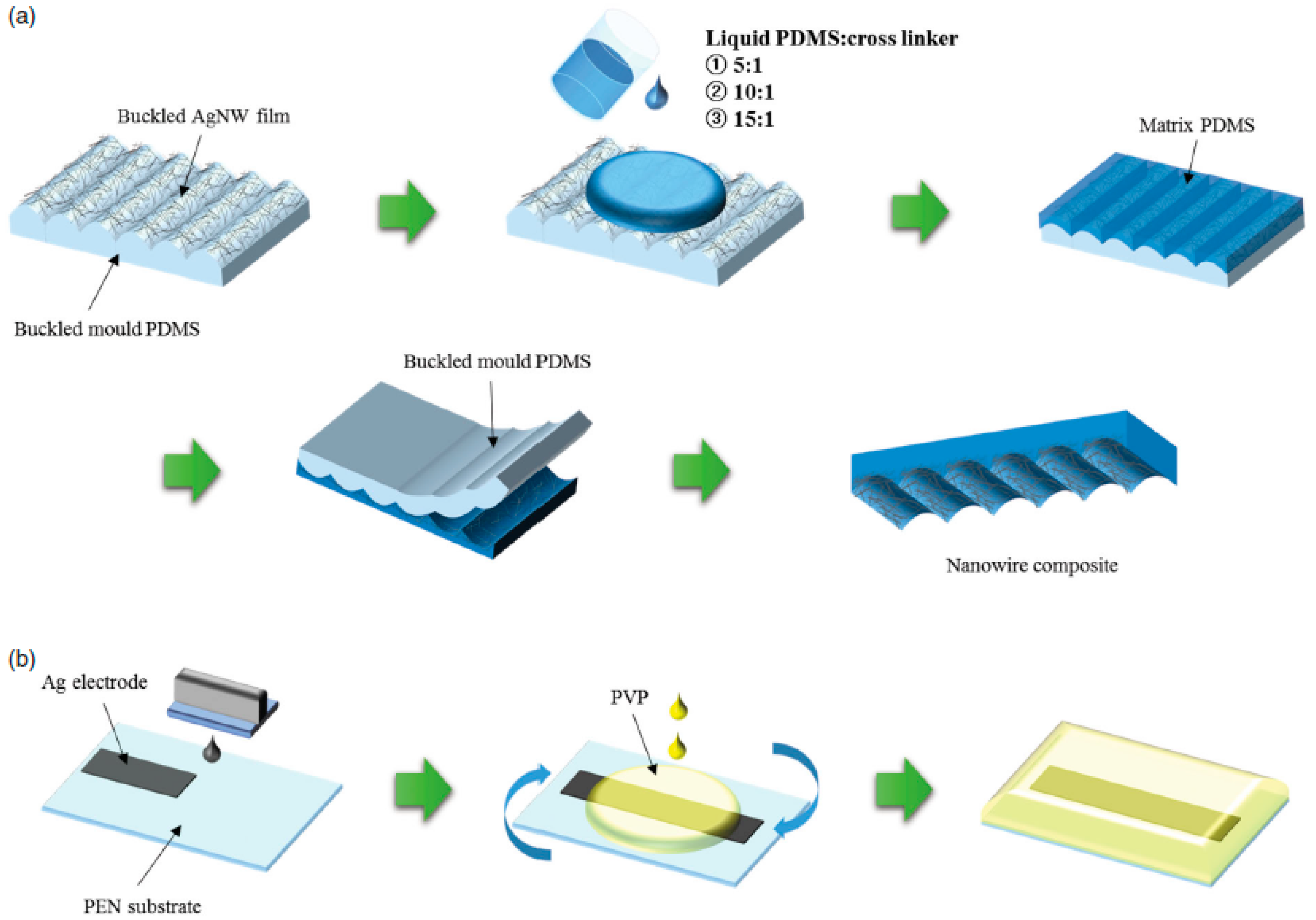
- Joo, Y.; Yoon, J.; Hong, Y. Elastomeric nanowire composite for flexible pressure sensors with tunable sensitivity. J. Inf. Disp. 2016, 17, 59–64. [Google Scholar] [CrossRef]
- Polzinger, B.; Keck, J.; Matic, V.; WEberhardt, H.K. Inkjet and Aerosol Jet Printed Sensors on 2D and 3D Substrates. In Proceedings of the Sensor, Nürnberg, Germany, 19–21 May 2015; pp. 566–569. [Google Scholar] [CrossRef]
- Gong, N.-W.; Hodges, S.; Paradiso, J.A. Leveraging conductive inkjet technology to build a scalable and versatile surface for ubiquitous sensing. In Proceedings of the 13th international conference on Ubiquitous computing, Beijing, China, 17–21 September 2011. [Google Scholar] [CrossRef]
- Joo, Y.; Byun, J.; Seong, N.; Ha, J.; Kim, H.; Kim, S.; Kim, T.; Im, H.; Kim, D.; Hong, Y. Silver nanowire-embedded PDMS with a multiscale structure for a highly sensitive and robust flexible pressure sensor. Nanoscale 2015, 7, 6208–6215. [Google Scholar] [CrossRef] [PubMed]
- Gong, N.-W.; Steimle, J.; Olberding, S.; Hodges, S.; Gillian, N.E.; Kawahara, Y.; Paradiso, J.A. PrintSense: A Versatile Sensing Technique to Support Multimodal Flexible Surface Interaction. In Proceedings of the SIGCHI Conference on Human Factors in Computing Systems, Toronto, ON, Canada, 26 April–1 May 2014; pp. 1407–1410. [Google Scholar] [CrossRef]
- El-Molla, S.; Albrecht, A.; Cagatay, E.; Mittendorfer, P.; Cheng, G.; Lugli, P.; Salmerón, J.F.; Rivadeneyra, A. Integration of a Thin Film PDMS-Based Capacitive Sensor for Tactile Sensing in an Electronic Skin. J. Sens. 2016, 2016, 1736169. [Google Scholar] [CrossRef]
- ORNL. Photonic Curing of Metal Films for Direct-Write Sensor Development; Technical Collaboration of ORNL and NovaCentrix_Final Report; ORNL: Oak Ridge, TN, USA, 2014. [Google Scholar]
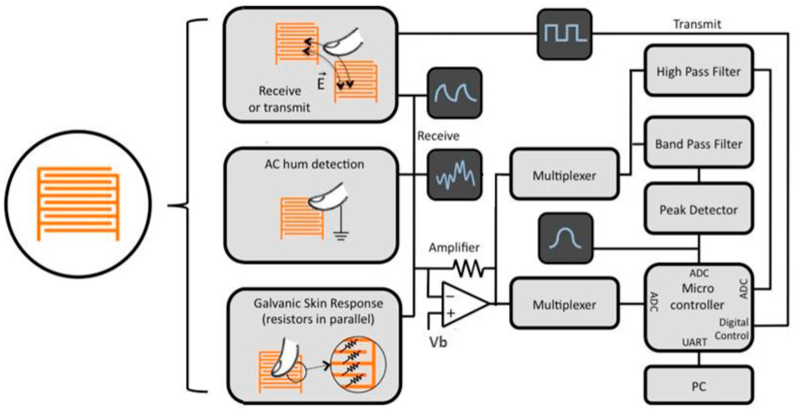
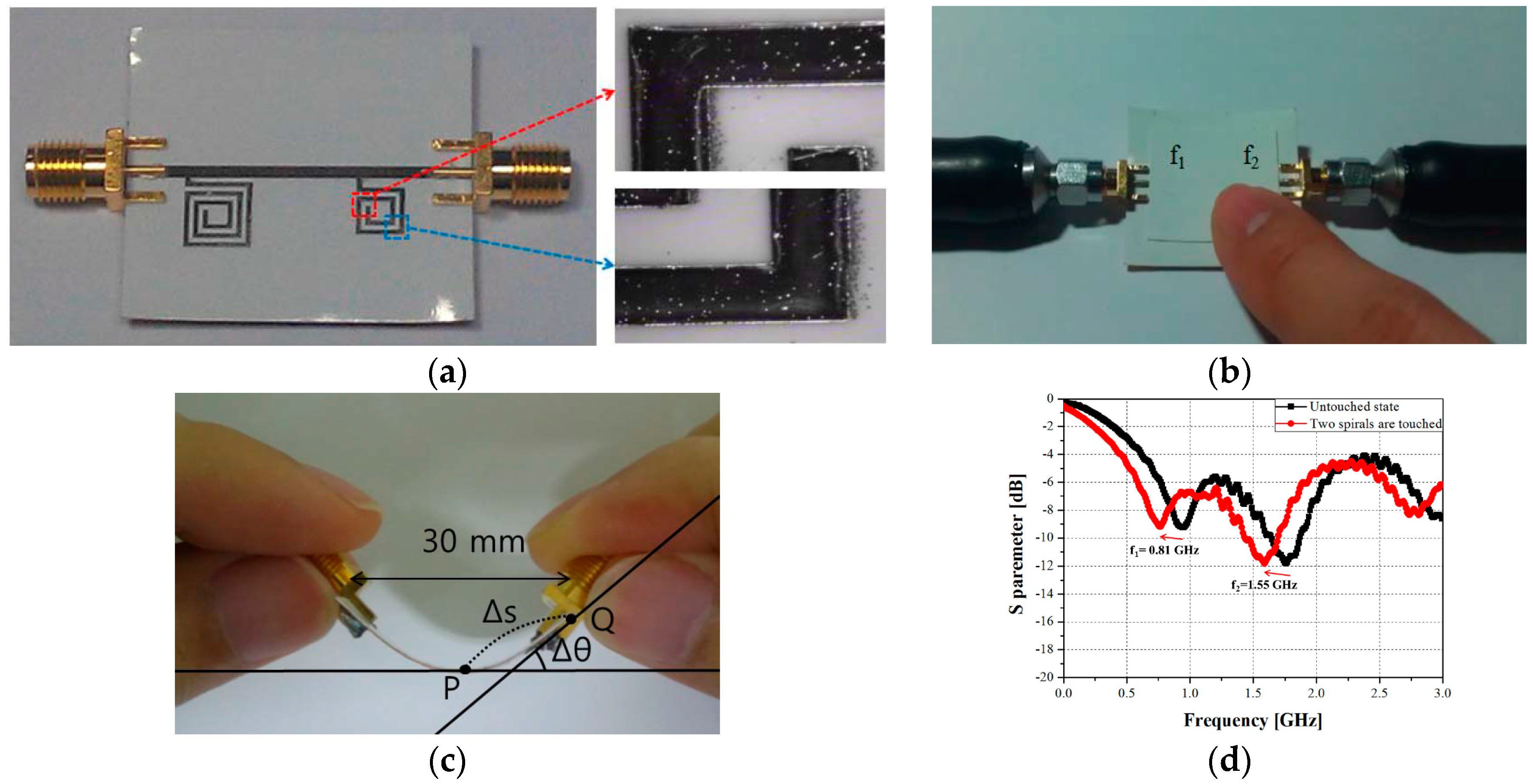
- Choi, S.; Eom, S.; Tentzeris, M.M.; Lim, S. Inkjet-Printed Electromagnet-Based Touchpad Using Spiral Resonators. J. Microelectromech. Syst. 2016, 25, 947–953. [Google Scholar] [CrossRef]
- Karataş, Ç.; Gruteser, M. Printing multi-key touch interfaces. In Proceedings of the 2015 ACM International Joint Conference on Pervasive and Ubiquitous Computing, Osaka, Japan, 7–11 September 2015; pp. 169–179. [Google Scholar] [CrossRef]
- Olberding, S.; Gong, N.-W.; Tiab, J.; Paradiso, J.A.; Steimle, J. A cuttable multi-touch sensor. In Proceedings of the 26th Annual ACM Symposium on User Interface Software and Technology—UIST ’13, St. Andrews, UK, 8–11 October 2013; pp. 245–254. [Google Scholar] [CrossRef]
- Ramakers, R.; Todi, K.; Luyten, K. PaperPulse: An Integrated Approach for Embedding Electronics in Paper Designs. In Proceedings of the SIGGRAPH ‘15, Los Angeles, CA, USA, 9–13 August 2015; pp. 2457–2466. [Google Scholar] [CrossRef]
- Yun, T.; Eom, S.; Lim, S. Paper-Based Capacitive Touchpad Using Home Inkjet Printer. J. Disp. Technol. 2016, 12, 1411–1416. [Google Scholar] [CrossRef]
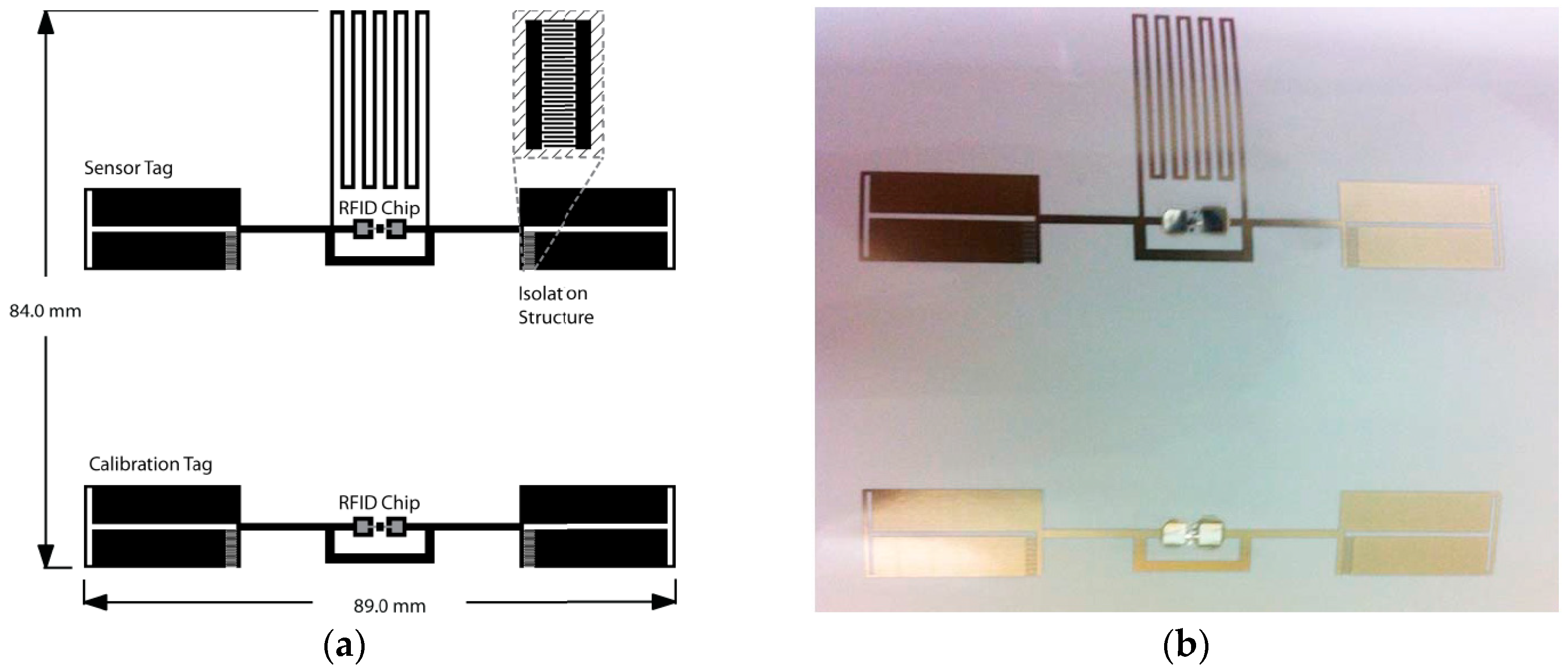
- Cook, B.S.; Vyas, R.; Kim, S.; Thai, T.; Le, T.; Traille, A.; Aubert, H.; Tentzeris, M.M. RFID-based sensors for zero-power autonomous wireless sensor networks. IEEE Sens. J. 2014, 14, 2419–2431. [Google Scholar] [CrossRef]
- Arrese, J.; Vescio, G.; Xuriguera, E.; Medina-Rodriguez, B.; Cornet, A.; Cirera, A. Flexible hybrid circuit fully inkjet-printed: Surface mount devices assembled by silver nanoparticles-based inkjet ink. J. Appl. Phys. 2017, 121. [Google Scholar] [CrossRef]
- Mazzeo, A.D.; Kalb, W.B.; Chan, L.; Killian, M.G.; Bloch, J.F.; Mazzeo, B.A.; Whitesides, G.M. Paper-based, capacitive touch pads. Adv. Mater. 2012, 24, 2850–2856. [Google Scholar] [CrossRef] [PubMed]


| Year | US Patents | European Patents | Chinese Patents | International |
|---|---|---|---|---|
| 1988–1997 | 57 | 1 | 0 | 1 |
| 1998–2007 | 147 | 1 | 2 | 1 |
| 2008–2017 | 276 | 4 | 47 | 177 |
| Property | Glass | Silicon | PDMS | Paper |
|---|---|---|---|---|
| Surface profile | Very low | Very low | Very low | Moderate |
| Flexibility | No | No | Yes | Yes |
| Structure | Solid | Solid | Solid, gas-permeable | Fibrous |
| Sensitivity to moisture | No | No | No | Yes |
| Disposability | No | No | No | Yes |
| High-throughput fabrication | Yes | Yes | No | Yes |
| Functionalization | Difficult | Moderate | Difficult | Easy |
| Homogeneity of material | Yes | Yes | Yes | No |
| Price | Moderate | High | Moderate | Low |
| Initial investment | Moderate | High | Moderate | Low |
| Substrates | ε | tanδ | Ref. # |
|---|---|---|---|
| Kodak Photo Paper | 2.85 | 0.05 | [29] |
| PDMS | 2.8 | 0.05 | [30] |
| Kapton film | 3 | 0.04 | [31] |
| Cotton | 1.6 | 0.04 | [32] |
| Polyester | 1.9 | 0.0045 | [32] |
| Ink Material | Conductivity | Permittivity | Ref. # |
|---|---|---|---|
| Ag nanoparticle | 0.4 to 2.5 × 10⁷ S/m | N/A | [29] |
| PVP dielectric ink | N/A | 11.7 | [25] |
| PEDOT:PSS | 3 × 10⁴ S/m | N/A | [24] |
| Graphene | 1 × 10⁸ S/m | N/A | [24] |
| SU-8 (dielectric layer) | N/A | 4.2 | [44] |
| Cu | 5.96 × 10⁷ S/m | N/A | [45] |
| Au | 4.42 × 10⁷ S/m | N/A | [45] |
| Ref. # | Nanoparticle Ink | Inkjet Printer | Substrate | Resolution | Sintering | Resistivity |
|---|---|---|---|---|---|---|
| [49] | In2O3 | Electrohydrodynamic inkjet | Flexible plastic | 2 µm | 250 °C @ 150 min | N/S |
| [50] | Ag | Dimatix 2831 | Si | 2 µm | 180 °C @ 30 min | N/S |
| [51] | Ag | Epson C110 | Chrome paper | 5 µm | 160 °C @ 30 min | 9.18 × 10⁻⁸–8.76 × 10⁻⁸ Ω·m |
| Ref. # | Ink Material | Substrate | Resistance or Resistivity |
|---|---|---|---|
| [64] | Cu | Flexible plastic | 200 mΩ/sq |
| [65] | Ag | Arylite | Resistance of AgNW film = 20 Ω |
| [67] | Ag | PDMS | Sheet Resistance of printed electrode = 19.2 ± 2.2 Ω/sq |
| [70] | Ag | Paper | Sheet Resistance = 0.19 Ω/sq |
| [71] | Ag | Paper | Sheet Resistance = 0.21 Ω/sq |
| [42] | PEDOT:PSS | Glass | Resistance across the ends of electrode = 6.9 K Ω |
© 2017 by the authors. Licensee MDPI, Basel, Switzerland. This article is an open access article distributed under the terms and conditions of the Creative Commons Attribution (CC BY) license (http://creativecommons.org/licenses/by/4.0/).
Share and Cite
Salim, A.; Lim, S. Review of Recent Inkjet-Printed Capacitive Tactile Sensors. Sensors 2017, 17, 2593. https://doi.org/10.3390/s17112593
Salim A, Lim S. Review of Recent Inkjet-Printed Capacitive Tactile Sensors. Sensors. 2017; 17(11):2593. https://doi.org/10.3390/s17112593
Chicago/Turabian StyleSalim, Ahmed, and Sungjoon Lim. 2017. "Review of Recent Inkjet-Printed Capacitive Tactile Sensors" Sensors 17, no. 11: 2593. https://doi.org/10.3390/s17112593
APA StyleSalim, A., & Lim, S. (2017). Review of Recent Inkjet-Printed Capacitive Tactile Sensors. Sensors, 17(11), 2593. https://doi.org/10.3390/s17112593