1. Introduction
Memristor is a new circuit element postulated by Leon Chua in 1971 [
1] and fabricated recently by the Stanley Williams group [
2] from Hewlett-Packard (HP). It exhibits excellent features of both memory [
3,
4,
5,
6] and neuromorphic applications [
2,
7,
8,
9,
10,
11]. For memory applications, it is nonvolatile and has an extremely small size of a few nanometers [
3,
4,
5]. For neuromorphic applications, it has features of pulse-based operation and adjustable resistance, which are ideal for tuning the synaptic weights of neuromorphic cells [
2,
7,
8,
9,
10,
12,
13].
A convenient way of programming a memristor with a certain value is by applying a rectangular voltage pulse whose magnitude of voltage is constant during pulse period and zero during non-pulse period. However, the variation of its resistance is a nonlinear function of the applied voltage pulse width even it is a linear model. We call the resistance of memristor memristance.
Fortunately, when two memristors with opposite polarities are combined together, the nonlinearity of memristance is reduced dramatically due to the complementary action of two memristors. Kim et al. presented an efficient weighting circuit for synaptic operation by building a bridge structure combining two opposite anti-serial memristor circuits [
7].
Waser’s group reported a fabrication result of complementary resistive switch (CRS) consisting of two back-to-back (anti-serial) memristive elements for the construction of large passive crossbar arrays by solving the sneak path problem [
14]. Later, the CRS architecture has been further investigated via an analytical approach [
15]. T. Liu et al. also reported the Current-Voltage (I-V) characteristics of antiparallel resistive switches (APRS) that strongly depend on the parameters of the individual switches [
16].
In this paper, we propose a linearized programming method utilizing an anti-serial architecture. To program a target memristor, the same type of a subsidiary memristor is prepared and connected to the target memristor in series with opposite polarity. Since composite memristance of the anti-serial circuit is a constant value, the current through the circuit is constant. It follows that the memristance variation of the individual memristor is a linear function of pulse width since the memristance variation is a linear function of charge.
The principle of such linear programming is explained theoretically and verified via simulations in this paper.
Section 2 describes a reason that memristor is a useful element for building a neural synapse.
Section 3 demonstrates nonlinearity in programing of a memristor with rectangular voltage pulses. To resolve the nonlinearity problem of voltage controlled memristor, an anti-serial architecture is proposed in
Section 4. Simulation results to support the proposed idea are provided in
Section 4.
Section 5 is the conclusion.
2. Memristor as a Promising Element for the Implementation of Neural Synapses
In biological neural systems, each neuron is connected to other neuron through a synapse between them. A synapse is a very special place in a neural cell, where memory and analog multiplication are performed.
Figure 1 shows input and output connections of a biological neuron where inputs (dendrites) are denoted as “b” and output (axon) is denoted as “a”. Typically, about 10,000 inputs (dendrites) are connected at a single neuron. Thus, the same number of synaptic weights is needed in a neuron. Therefore, the implementation of huge number of neural synapses in a chip is a big roadblock for the development of an artificial neuron system. To make matters worse, one synaptic circuit is composed of many transistors as shown in
Figure 2. Therefore, the implementation of an artificial neural system that mimics a biological neural system is seemingly far beyond our reach with the current circuit technologies.
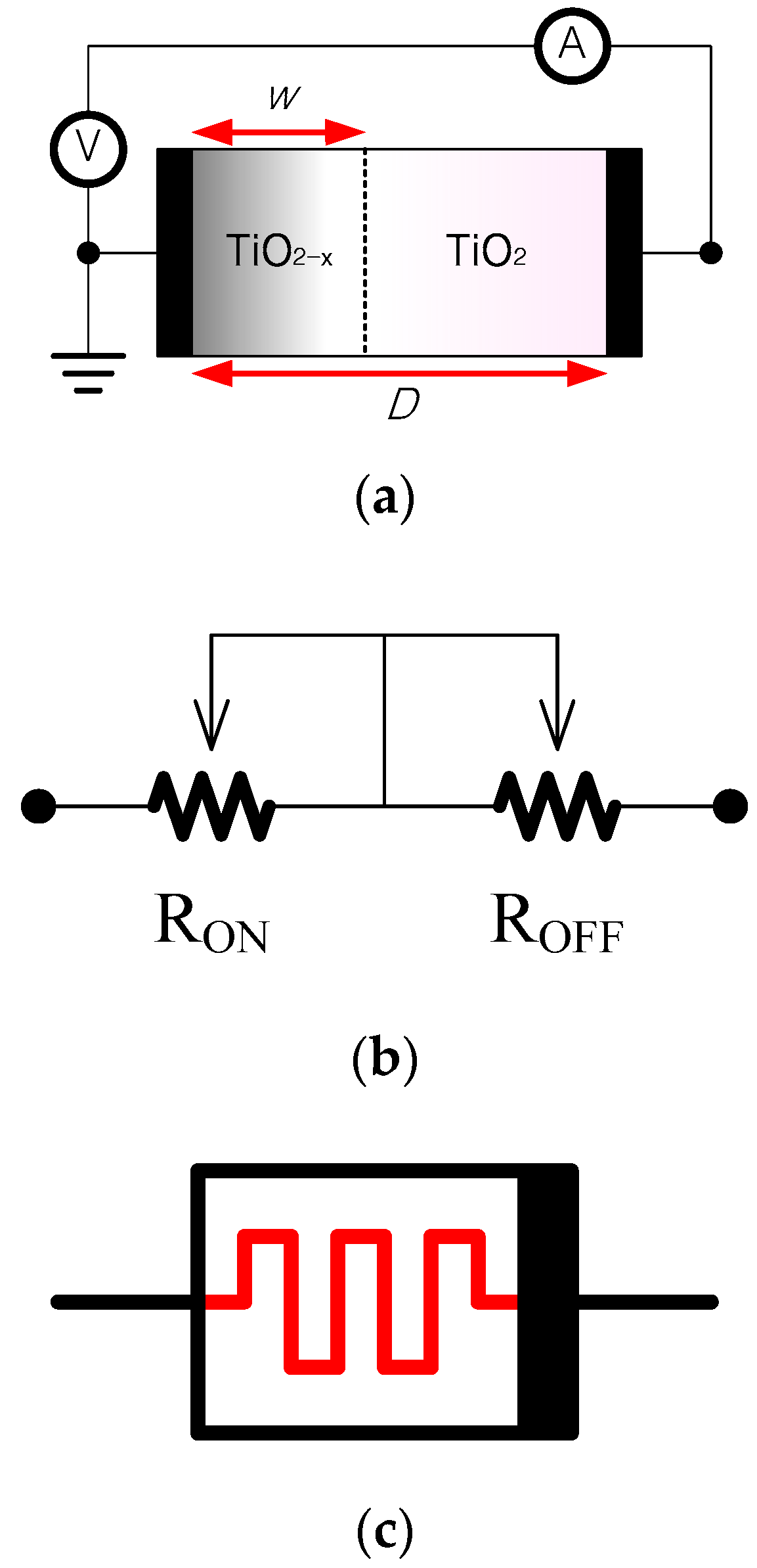
Figure 3 shows a structure of a memristor fabricated successfully by HP [
2]. In an HP TiO
2 (Titanium dioxide) memristor model [
2], an undoped region with highly resistive TiO
2 and a doped region with a highly conductive oxygen vacancy TiO
2−x layer are sandwiched between two platinum electrodes. When a voltage or current signal is applied to the device, the border line between the doped and undoped layers shifts as a function of the applied voltage or current. In consequence, the resistance between the two electrodes is altered.
Figure 3b,c are equivalent circuits.
In the TiO2 memristor, a thin titanium dioxide (TiO2) layer and a thin oxygen-poor titanium dioxide (TiO2−x) layer are sandwiched between two platinum electrodes. When a voltage or current is applied to the device, the resistance between the two electrodes is altered.
The memristor is defined [
7] by
where
φ(
t) and
q(
t) denote the flux and charge, respectively, at time
t. Thus, the resistance can be interpreted as the slope at the operating point
at time
t on the memristor
curve. If the
curve is nonlinear; the resistance will vary with the operating point.
Since the flux
φ is defined by
, the resistance of the memristor, called the memristance,
, can be controlled by applying a voltage or current signal across the memristor, where
Equation (2) shows that a memristor is a kind of resistor that is variable depending upon an operation point on a charge and flux plane. In this sense, it is a programmable resistance.
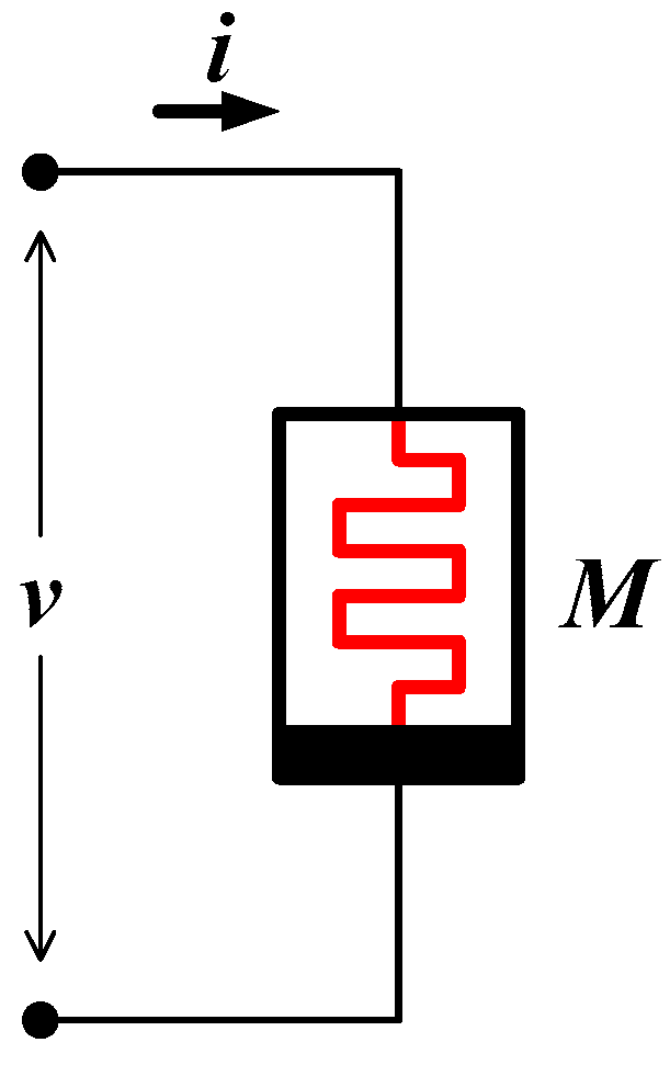
Let the input of a memristor be a current and the voltage across the memristor be the output of a single memristor circuit as shown in
Figure 4. Then, according to Ohm’s law, the voltage output is an analog multiplication between the current input and the resistance of a memristor as in Equation (3).
Therefore, memristor is, in fact, an analog multiplier. Note that the resistance of a memristor is distinguished from that of an ordinary resistor in the sense that its resistance is programmable. It follows that the resistance of a memristor is called memristance. Since the memristance of a memristor can be altered (programmed) by input voltage/current and an analog multiplication is performed within a single device, the memristor is known as an ideal element for the implementation of synapses.
3. Nonlinearity in Memristor
In the TiO2 memristor, a thin TiO2 layer and a thin oxygen-poor TiO2−x layer are sandwiched between two platinum electrodes. The TiO2 layer and the TiO2−x layer are referred to as un-doped, and doped layers, respectively. When a voltage or current is applied to the device, the dividing line between the TiO2 and TiO2−x layers shifts as a function of the applied voltage or current. As a result, the resistance between the two electrodes is altered.
Let D and denote the thickness of the sandwiched area and the doped area (oxygen deficient area) in the TiO2 memristor, respectively, and let and denote the resistances at high and low dopant concentration areas, respectively.
The relationship between the flux and the charge of the TiO
2 memristor is given by [
2]
where
µν is the dopant mobility and
is the state variable
x.
The memristance
of a memristor can be computed with
as
Assume that the applied input is a current
i(
t), then, Equation (5) is
The derivative of Equation (6) with respect to time gives
It follows from Equation (7)
Assume that a constant voltage
V is applied as an input voltage. Integrating both sides of Equation (8) results in
where
C is the constant of integration.
It follows from Equation (9) that
can be written as,
Equation (10) exhibits a fact that memristance is a nonlinear function of time t. Thus, programming the memristor with an arbitrary value is very difficult.
Differently from the linear drift model described above, the nonlinear phenomenon appears often at the boundaries of nano-scale devices; with even the small voltage applied across nanometer devices, a large electric field is produced, and, therefore, the ion boundary position is moved in a non-linear fashion in nano-scale devices [
14].
Several different types of nonlinear memristor models have been investigated [
11,
19,
20]. One of them is the window model in which the state equation is multiplied by window function
, namely
where
p is an integer parameter and
is defined by
This is called the nonlinear drift model or memristive model. It is difficult to find the solution satisfying both Equations (11) and (12) analytically. However,
can be computed numerically as
where Δ
q is the charge increment fed to the memristor during the time interval Δ
t and computed by integrating the input current as
Substituting the value of
from Equation (7) in Equation (8), we get
The current voltage relationship can be obtained as
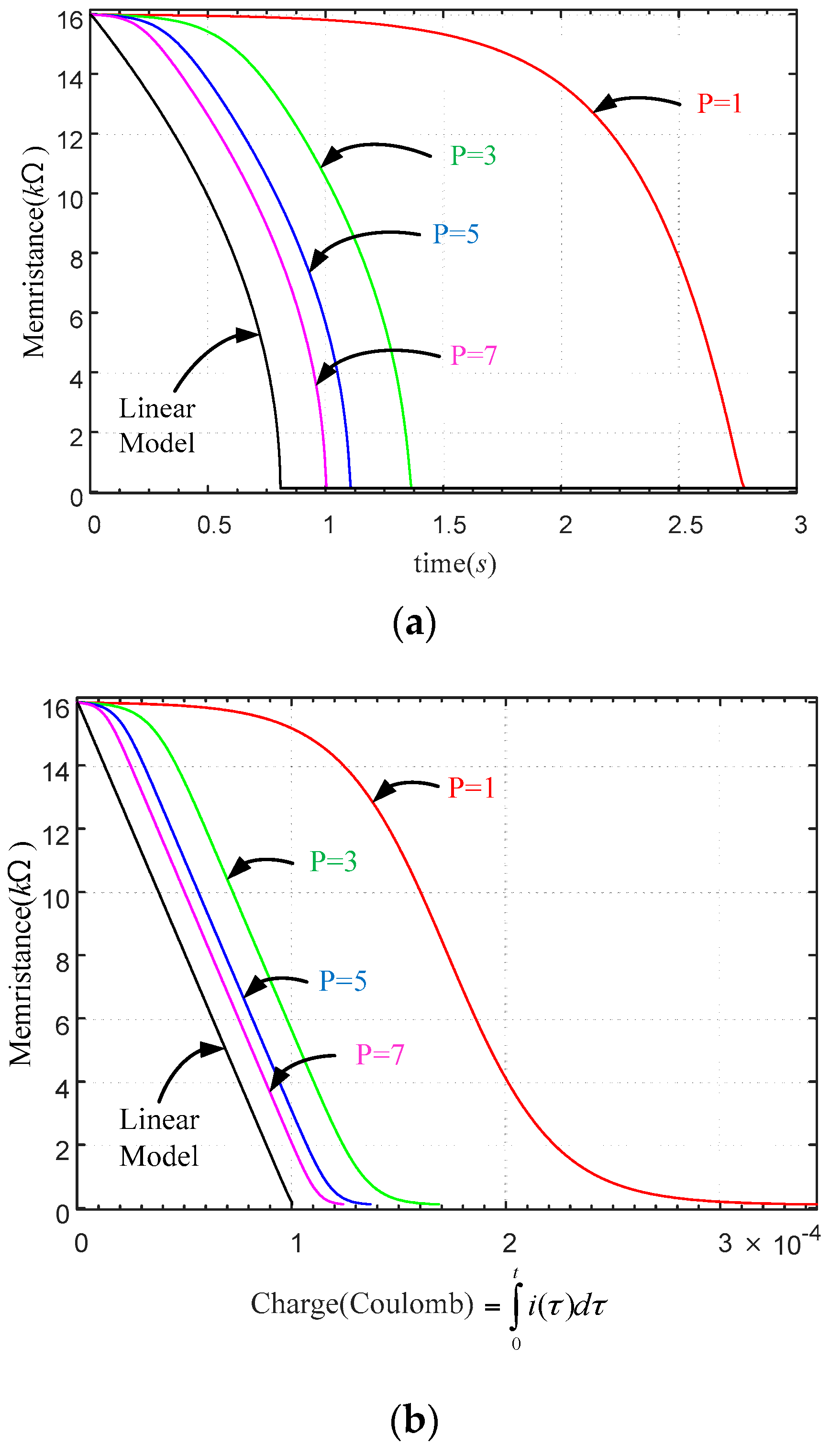
Figure 5 shows the graphs of the memristance vs. time and the memristance vs. time charge of the nonlinear models of memristors when a rectangular pulse is applied. The memristance is more nonlinear about time than that of charge. In addition, as the number
p becomes smaller, the nonlinearity increases. On the other hand, as the integer p increases, the model tends to the linear model.
4. Linearization in Memristor Programming with Anti-Serial Architecture
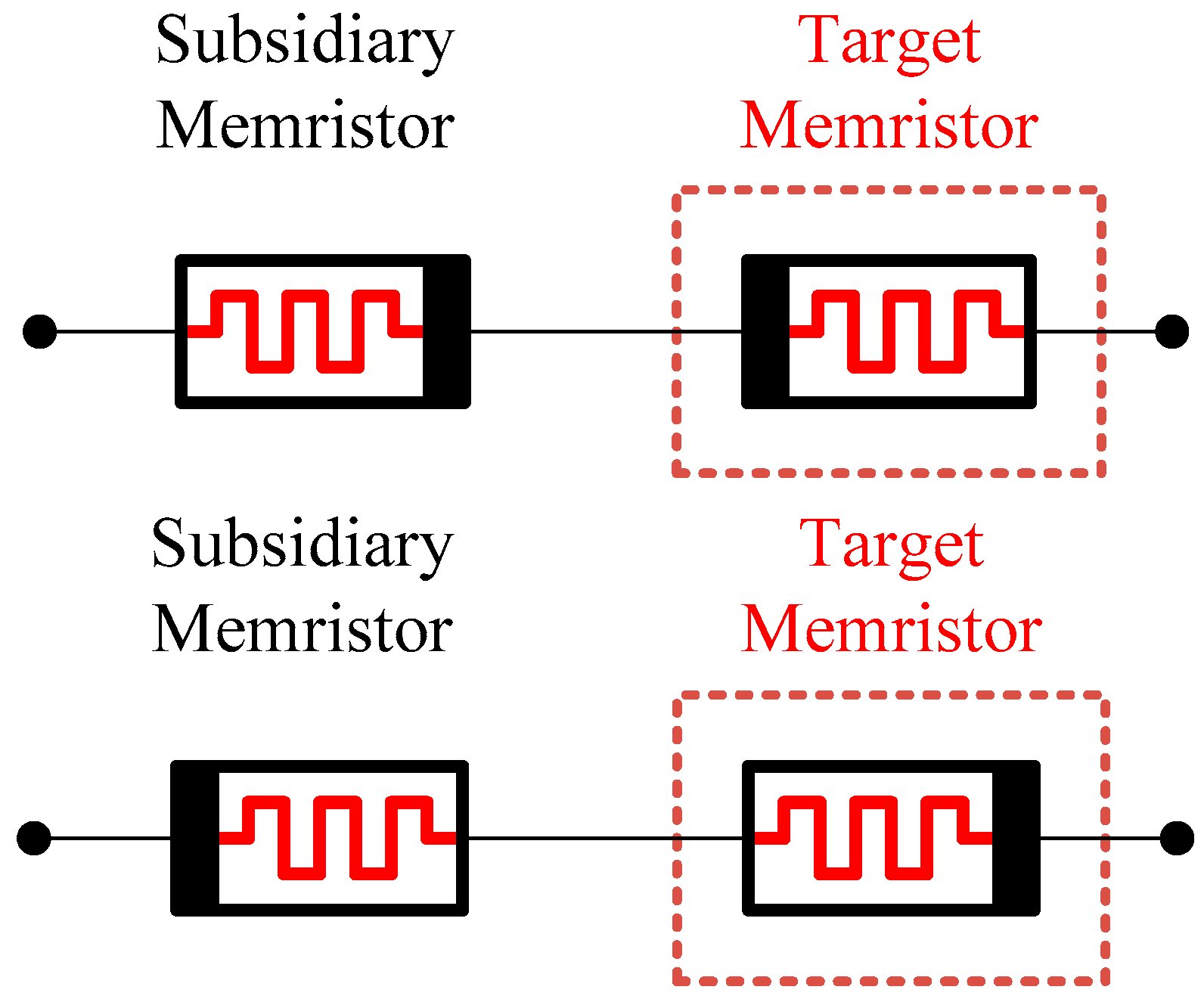
Anti-serial memristor circuit is a circuit of two memristors in serial connection with opposite polarities as shown in
Figure 6. When a positive voltage (or current) signal is applied to a circuit with two memristors connected in series, but with opposite polarities, then the memristance of M1 decreases, whereas the memristance of M2 increases. As a result, the composite memristance becomes constant, due to their complementary action [
21].
Let us assume that the polarity of M1 is the same as that of the predefined reference polarity, and the polarity of M2 is opposite to that of the reference. If charge
q(
t) is injected into the positive terminal of the composite device, it acts as positive charge for M1, whereas it acts as negative charge for M2. Thus,
Similarly, the sign of flux
is opposite to the reference, i.e.,
Thus, flux
and
of memristor M1 and M2 can be written as functions of charge
q(
t), as
The total flux is the sum of and .
When two memristors are assumed to be identical, and they are in the stable composite memristance state, the flux of the composite memristor becomes
where
. Furthermore, the memristance of the composite memristor can be obtained by differentiating Equation (21) with respect to
q(
t), as
where,
is the composite memristance, and
is a constant value of
.
Note that in Equation (22) is a constant, since all the related parameters of are constant.
Let M2 is a target memristor to program. From Equation (6), the expression of memristance
MTarget is
when a rectangular voltage pulse with V volt is applied, current
i(
t) during a non-zero pulse period can be computed as
Plugging Equation (24) into Equation (23), we obtain
All the parameters of the right side of Equation (25) are constant except time t. Therefore, it is a linear function of time. Comparing Equations (25) with (10) which is a nonlinear equation about time t, programing a memristor with Equation (25) is much easier than with Equation (10).
To program a target memristor with this method, the same type of a subsidiary memristor is prepared and connected to the target memristor in series with opposite polarity as in
Figure 7. Since composite memristance of the anti-serial circuit is a constant value, the current through the circuit is constant. It follows that the memristance variation of the individual memristor is a linear function of pulse width since the memristance variation is a linear function of charge.
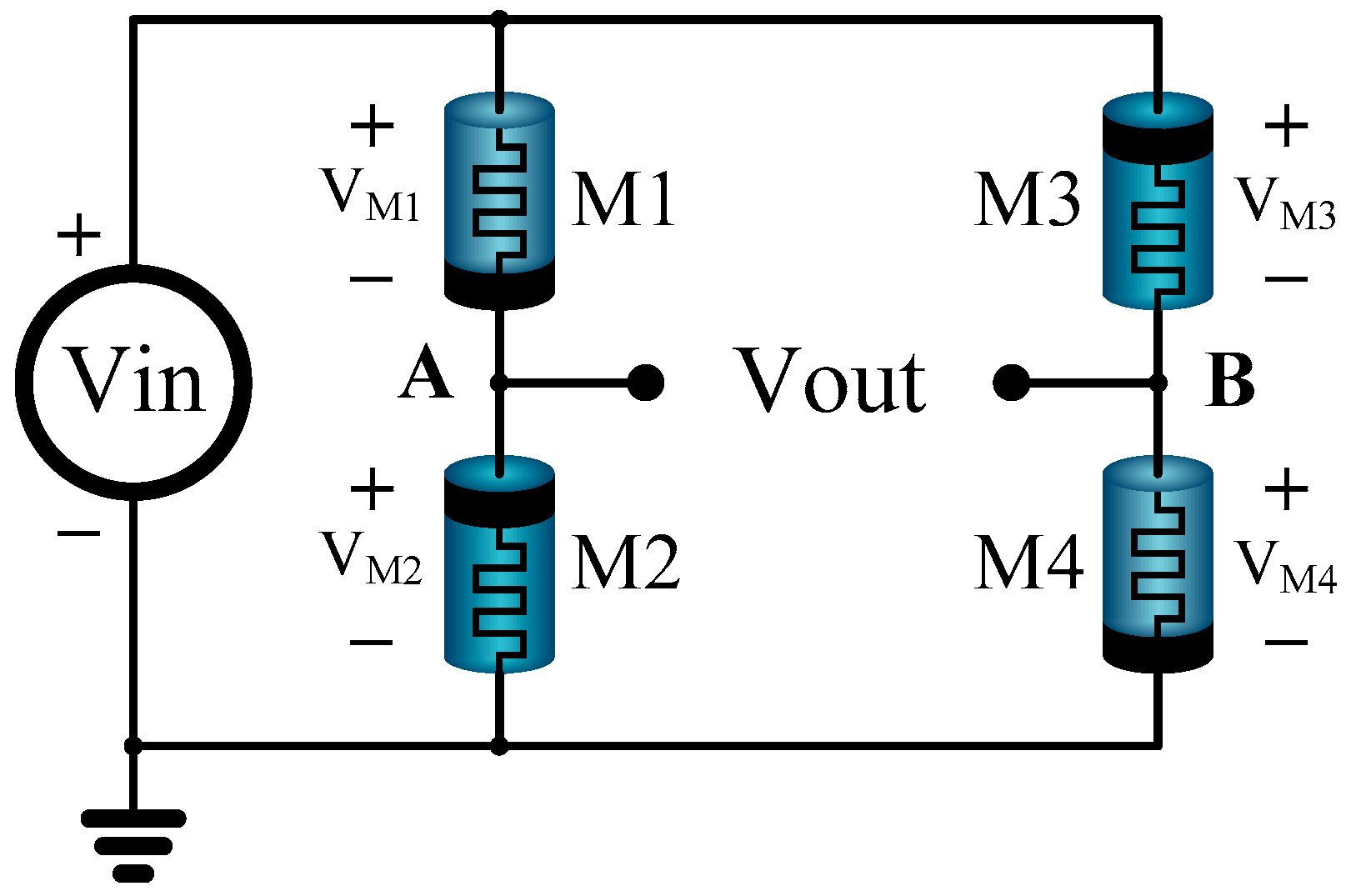
5. Application of the Anti-Serial Memristor Architecture to the Weight Programming of a Memristor Bridge Synapse
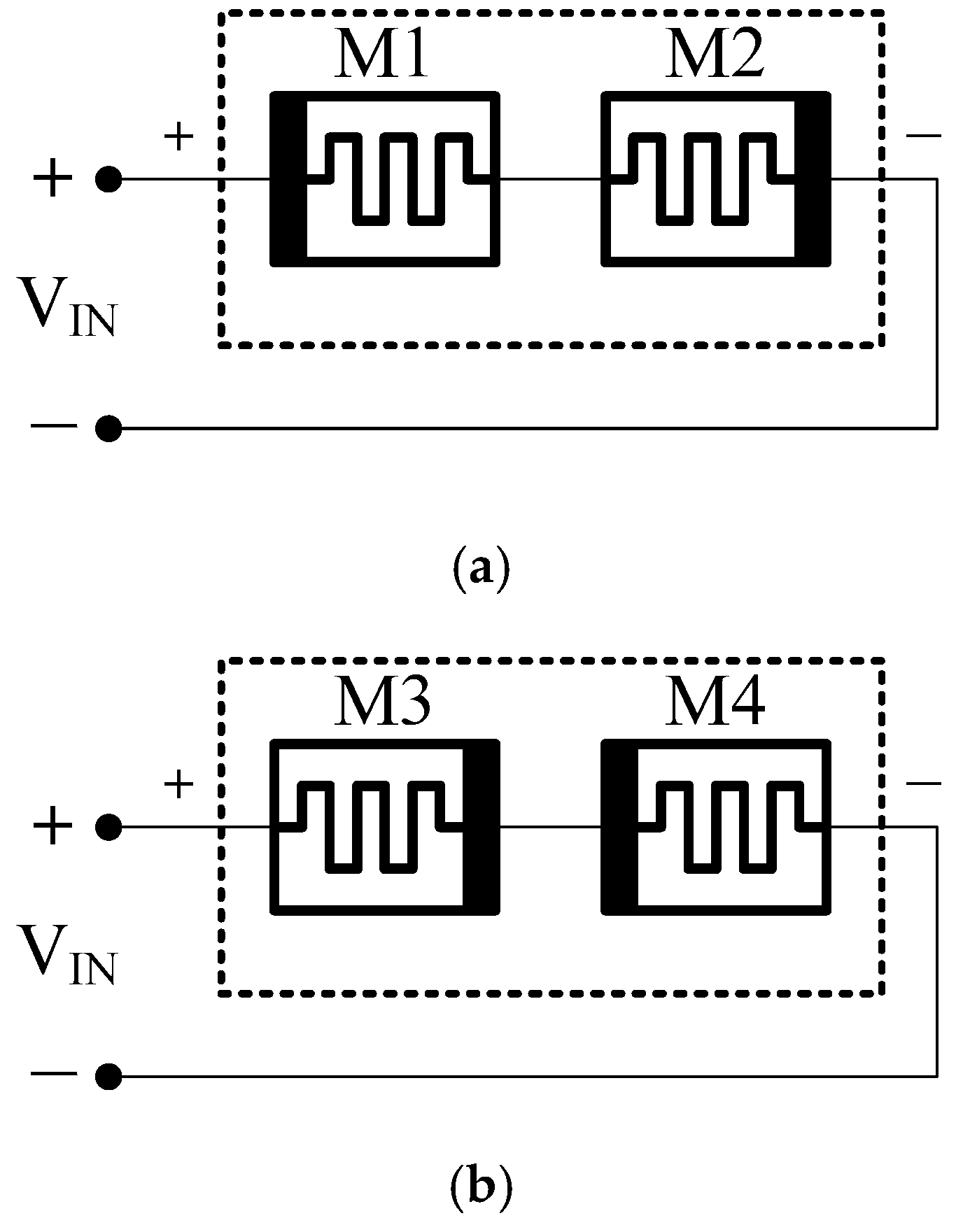
Anti-serial connections of memristor circuit are utilized to build a memristor bridge weighting circuit [
7], which can be programmed linearly due to the cooperation of two sets of anti-serial memristor circuits.
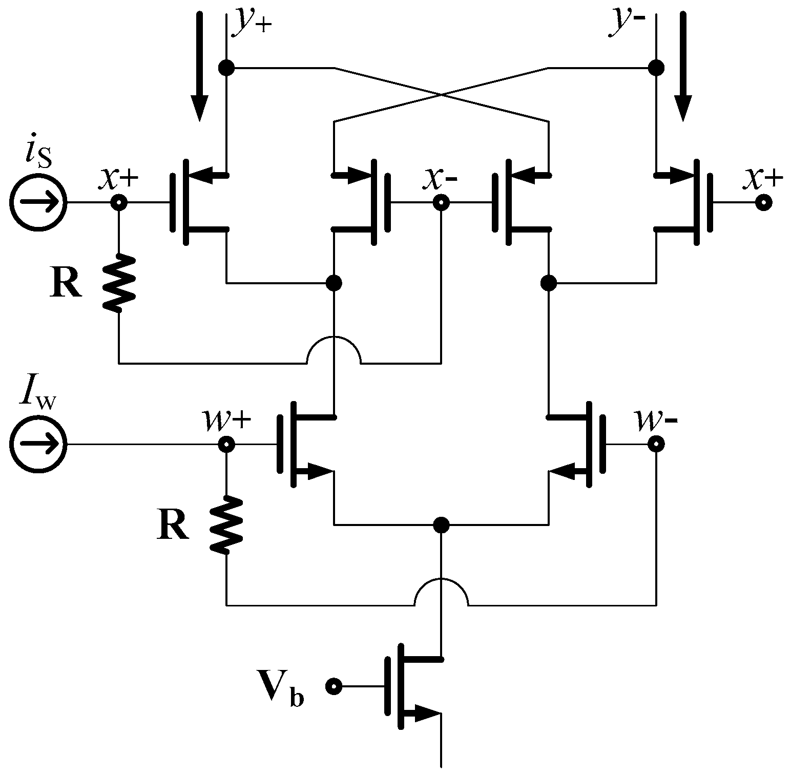
The memristor bridge circuit consists of four identical memristors with different polarities indicated in
Figure 8. When a positive or a negative pulse
is applied at the input, the memristance of each memristor is increased or decreased linearly depending upon its polarity. For instance, when a positive pulse is applied as input, the memristances of M1 and M4 (whose polarities are forward-biased) will decrease. On the other hand, the memristances of M2 and M3 (whose polarities are reverse-biased) will increase. It follows that the voltage
at
node A (with respect to ground) becomes larger than the voltage
at
node B for a positive input signal pulse. In this case, the circuit produces a positive output voltage
representing a positive synaptic weight.
On the other hand, when a negative strong pulse is applied, the memristances are varied in the opposite direction and the voltage at node B becomes larger than that at node A. In this case, the circuit produces a negative output voltage representing a negative synaptic weight.
6. Simulation
The linearity in programing with several memristor circuits such as single and anti-serial circuit has been tested. The memristor models employed for these simulations are a linear drift model of HP TiO
2 [
2] and a nonlinear model with window function with
p = 1 [
16].
When we want to program a memristor to a certain memristance value, one of the easiest ways is by applying a constant voltage or current for a certain length of time. If memristance variation about time is linear, the desired value of memristance can be programmed easily since the programmed memristance would be proportional to the width of a voltage pulse.
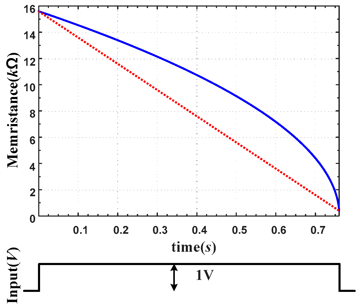
Figure 9 shows the memristance variation about time when a constant voltage of 1 V is applied to a TiO
2 memristor model. Though the memristance curve is linear about charge, it is non-linear about applied time (pulse width) as shown with a solid line in
Figure 9. Such a nonlinearity about time makes the programing of a memristor difficult. The desirable memristance curve is the dotted line.
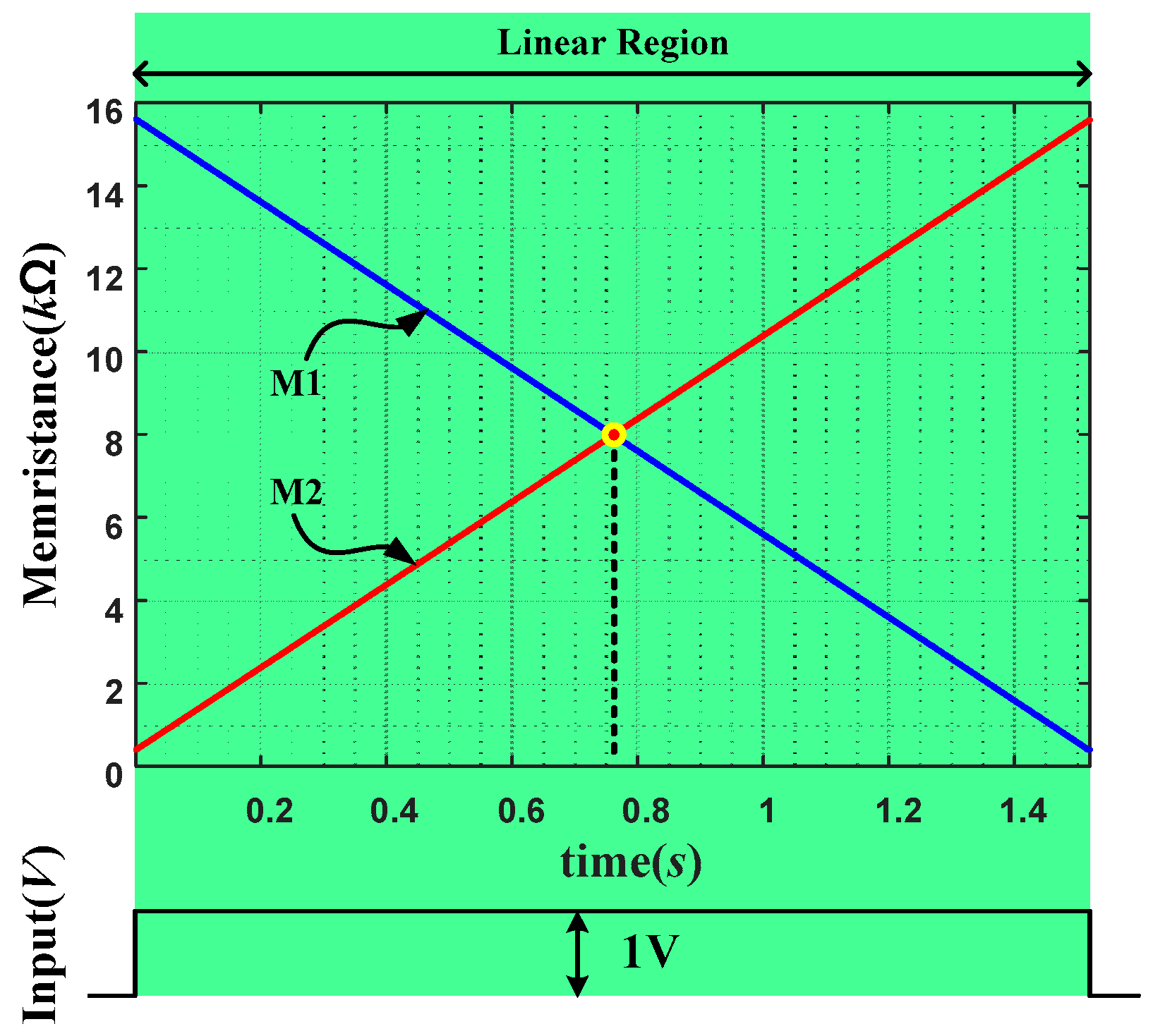
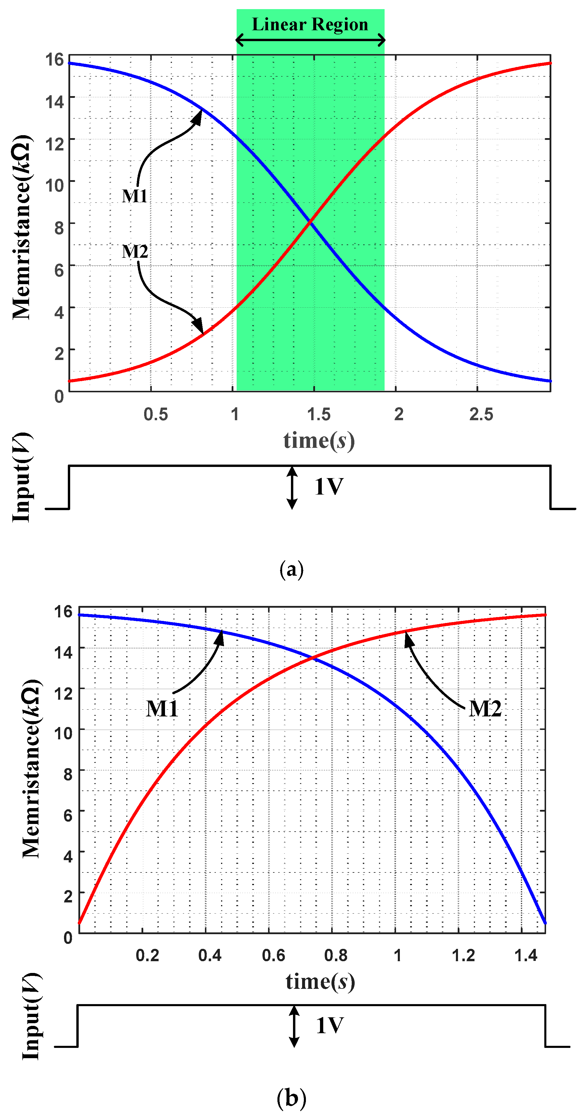
Figure 10 shows a memristance variations of two memristors in the proposed anti-serial connection in
Figure 7 when a constant voltage source is applied. Upon applying a constant voltage source to the anti-serial circuit, the subsidiary and target memristors are cooperating in complimentary fashion. The resultant memristance variation is linearized about time as shown in the figure.
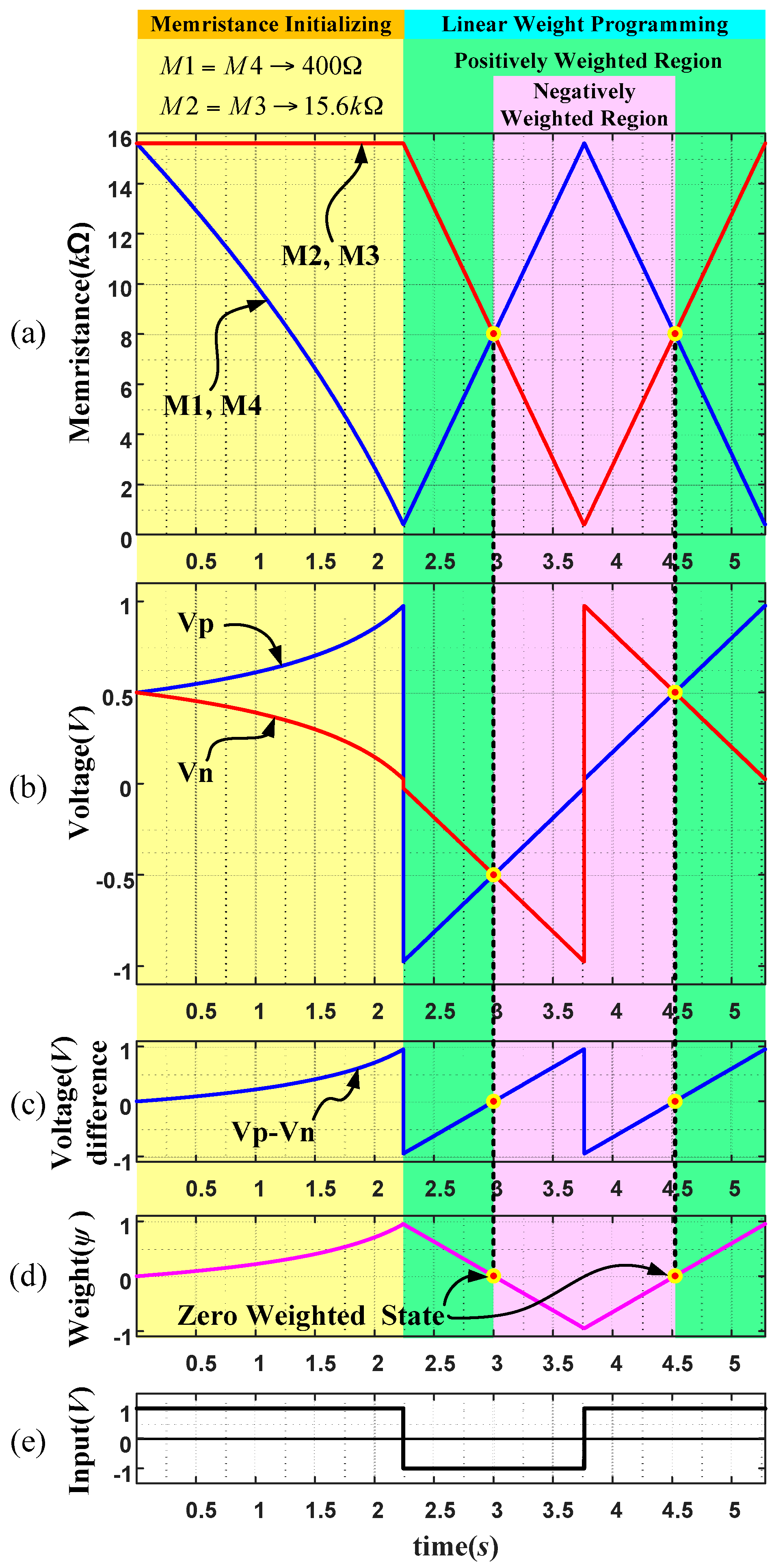
Simulations to demonstrate the linearity in programming the memristor bridge synapse circuit have also been performed. If the memristance variation of each memristor of anti-serial memristor circuit is linear, the voltage change at each node of the circuit is supposed to be linear. In consequence, the weight of the memristor bridge synapse can be programmed linearly since the memristor bridge synapse circuit is composed of two different sets of anti-serial circuits.
Figure 11 shows a weight programming scenario where
Figure 11a is the changes of two voltages (
Vp and
Vn) at middle points starting with 15.6 kΩ. When +1 V is applied for a long time as in
Figure 11e, memristances of M1 and M4 are reduced gradually until 400 Ω is reached while M2 and M3 are kept with its highest memristance 15.6 kΩ. The change of memristance is a nonlinear function about time during this period. Then, when −1 V is applied afterwards, the memristances of M2 and M3 are reduced linearly while those of M1 and M4 are increased until M2, M3 and M1, M4 reach the minimum and maximum values, respectively. Then, when +1 V is applied again, the memristances of M2 and M3 are increased while those of M1 and M4 are decreased linearly.
Figure 11b shows the changes of voltages
Vp and
Vn which are the voltages at middle points of two anti-serial circuits during the period of
Figure 11a. As seen in the middle of the figure, voltage changes linearly about time due to the linear change of memristances in
Figure 11a. As the result, the voltage difference of middle voltage (
Vp −
Vn) is also linear as in
Figure 11c and finally, weight changes of the memristor bridge synapses becomes also linear as in
Figure 11d.
The effect of the nonlinearity of memristor models to the performance of our memristor circuit has also been investigated.
Figure 12a shows the memristance variations for each memristor of anti-serially connected non-linear memristor circuit. It is assumed that M1 and M2 have initial values of 15.6 kΩ and 400 Ω, respectively. When a positive DC input with +1 V is applied at the anti-serial circuit, the memristance of M1 is reduced and that of M2 is increased. Observe the region at the middle where graphs are almost linear though some nonlinear regions can be seen at the end of the curves. Since weighting operations are performed only in the linear region at the center as indicated with a box, linear programming can be performed with the proposed anti-serial architecture. Meanwhile
Figure 12b is the variations of memristances when the programming signal is applied at individual memristors. As seen in the figure, the memristance changes as functions of time are highly nonlinear in all the range of the curves.
Comparing
Figure 12a and
Figure 12b, the memristances of anti-serial memristors are linearized significantly than those without the anti-serial connection.
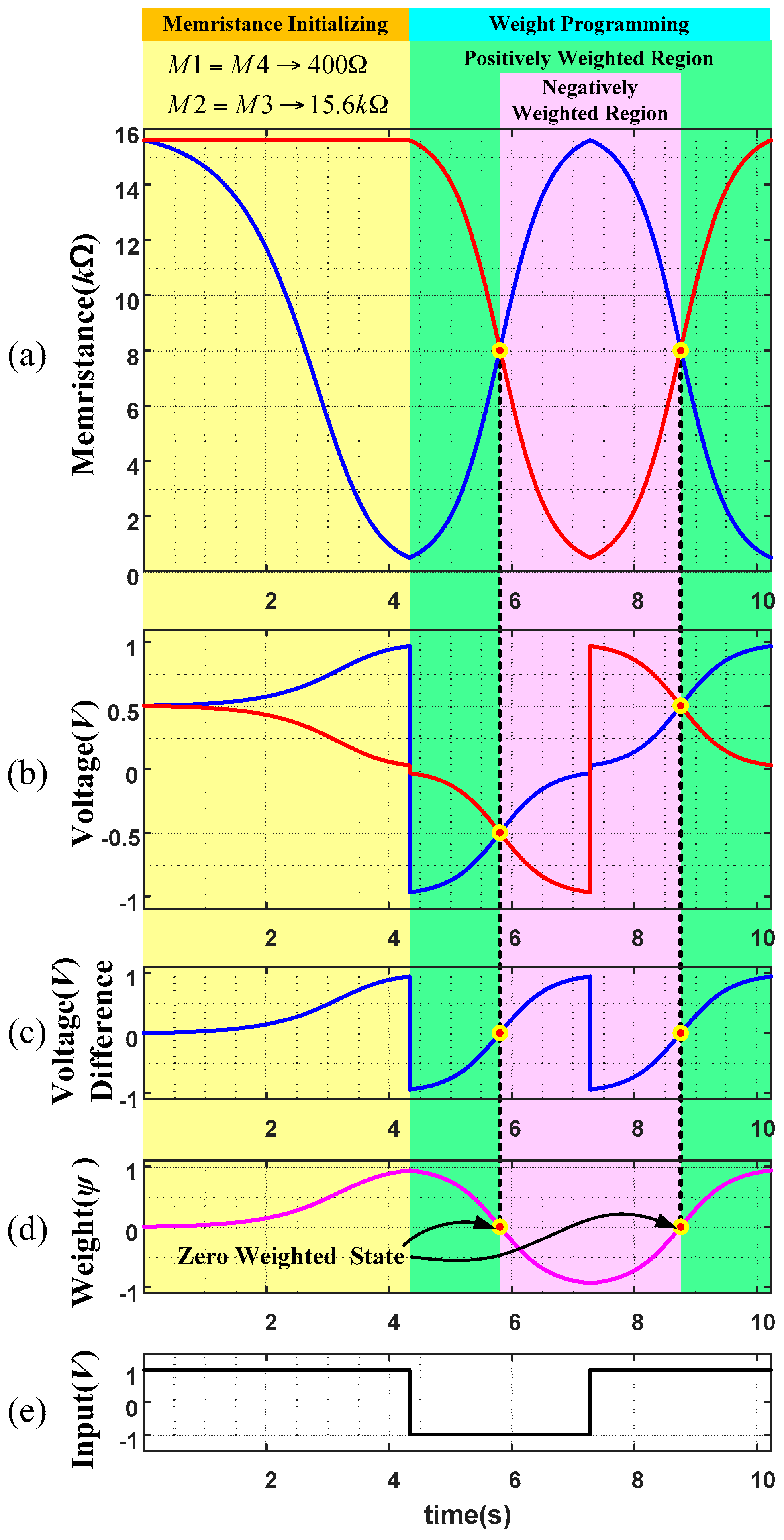
The effect of weight programming of memristor bridge synapses with non-linear model of memristors is also investigated.
Figure 13 shows parameter variation of a memristor bridge synapse while the programming input signal as in
Figure 13e is applied. All the necessary arrangements are the same as the linear memristor case in
Figure 11 except that nonlinear memristors are employed.
Observe the memristance especially in
Figure 13a and weight variation in
Figure 13d at the time periods of [5.355, 6.247] s and [8.318, 9.209] s are all linearized very much.
7. Conclusions
In neuromorphic applications of memristors, a linear programming of memristance about time is important. In this paper, we proposed a method utilizing an anti-serial architecture.
Anti-serial architecture is a serial connection of two memristors with opposite polarities. It exhibits linearization in programming due to a complimentary action of two memristors; when the memristance of one memristor increases, the other decreases. Since composite memristance of the anti-serial circuit is a constant value, the current through the circuit is constant. It follows that the memristance variation of the individual memristor is a linear function about pulse width since the memristance variation is a linear function of charge.
Our proposed idea of linear programming of a memristor is by employing an additional subsidiary memristor with an opposite polarity when programming a target memristor is needed. When programming a target memristor is needed, a subsidiary memristor with an opposite polarity is prepared so that the subsidiary and target memristors construct an anti-serial architecture.
The validity of the proposed idea has been proved with linear drift model of HP TiO2 memristor. In addition, it has been applied in building a memristor synapse circuit that is composed of two different sets of anti-serial architectures. Due to the anti-serial architecture, weights have been programmed linearly about applied pulse width.
The proposed architecture has also been tested with memristor models of highly nonlinear characteristics. Memristances of the anti-serial memristor circuits and weights of memristor bridge synapse circuits are all linearized significantly around zero memristance and zero weight regions, respectively.


