
A Low-Noise Transimpedance Amplifier for BLM-Based Ion Channel Recording

 ,
, 
Abstract
:1. Introduction
- A microfluidic device allowing stable, reliable and automatic BLM formation.
- A fast low-noise electronic interface ables to acquire pA currents.
- A compact, robust and scalable system containing an array of microfluidic devices and electronic interface.
2. Proposed Transimpedance Amplifier
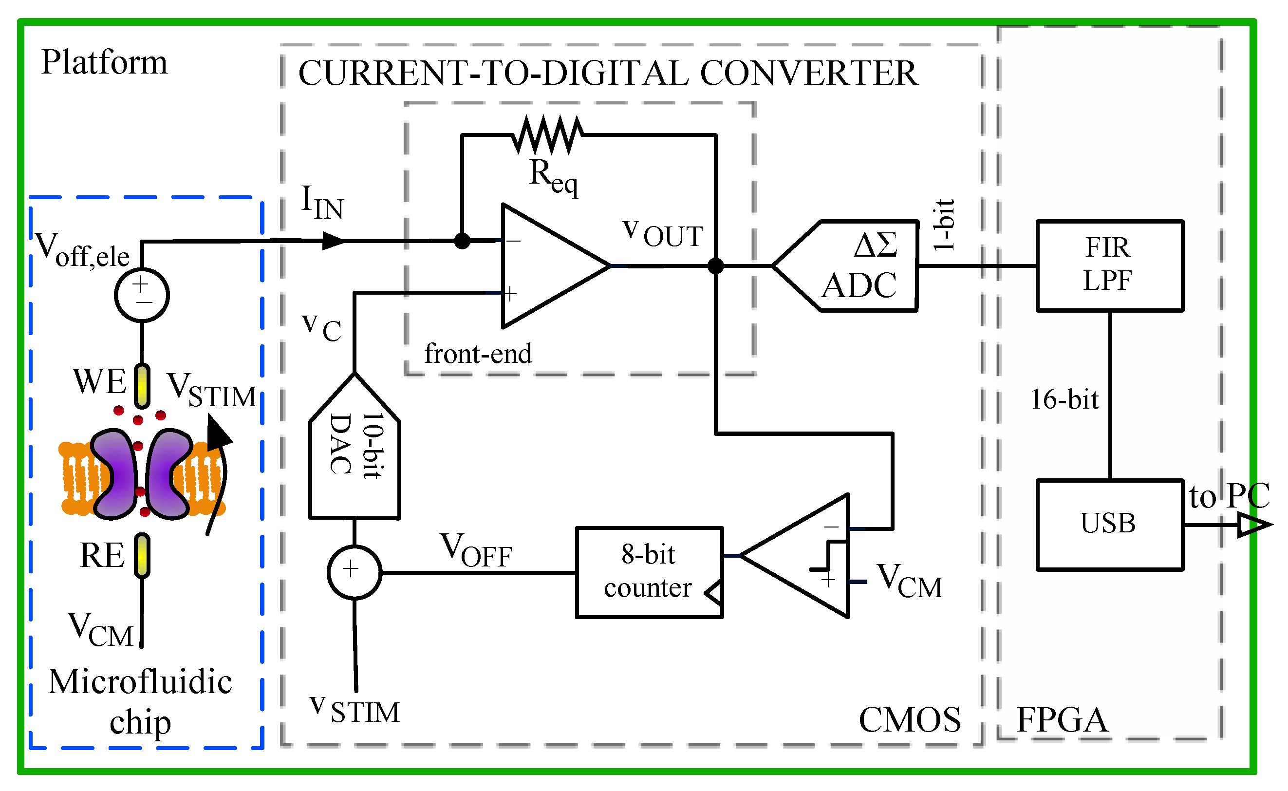
2.1. Ion Channel Recording Platform
- Three disposable microfluidic devices manufactured on a glass substrate holding 4 BLMs each [12].
- A small PCB hosting two CMOS 2-channel low-noise current-to-digital amplifiers that can measure pA currents.
- A motherboard with a digital control unit implemented in a Field Programmable Gate Array (FPGA) [11].
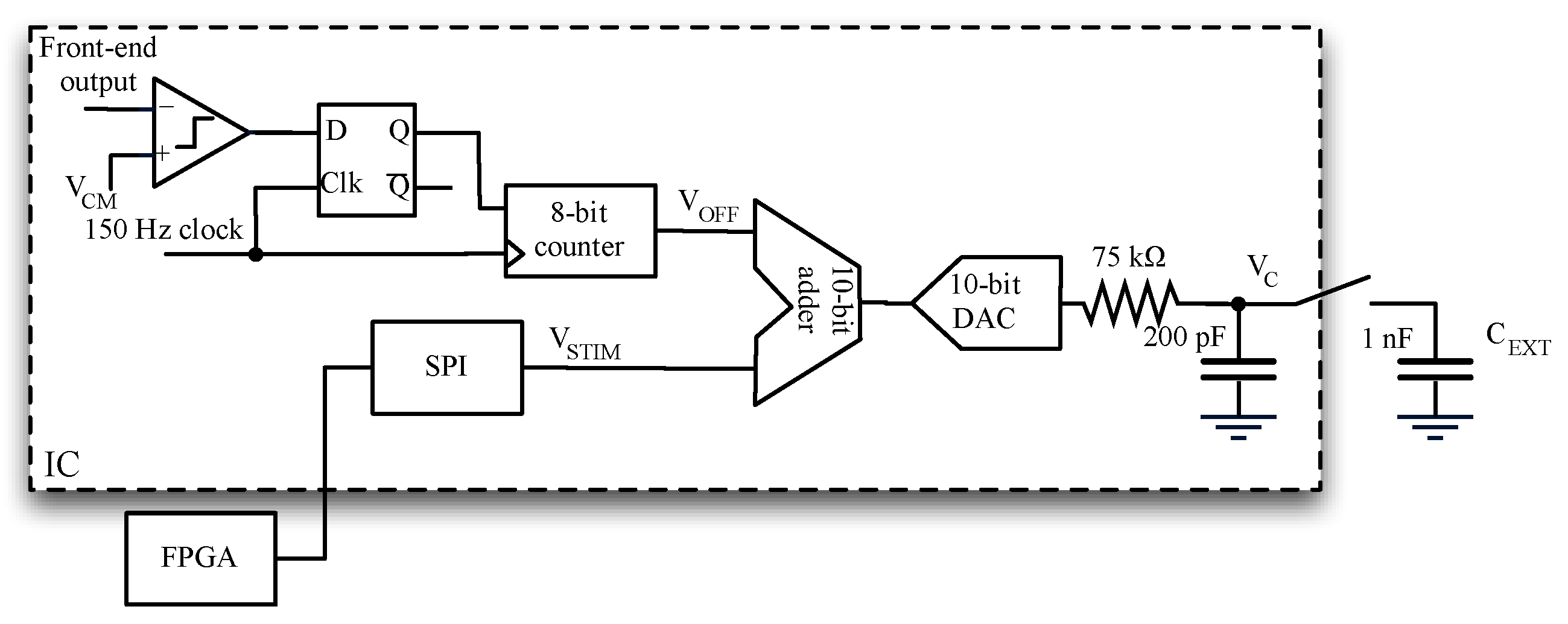
- Read the front-end output voltage VOUT;
- Compare VOUT with the reference voltage VCM;
- Change DC voltage VOFF so that it becomes equal to VCM + Voff,ele. (Note reference electrode is tight to VCM).
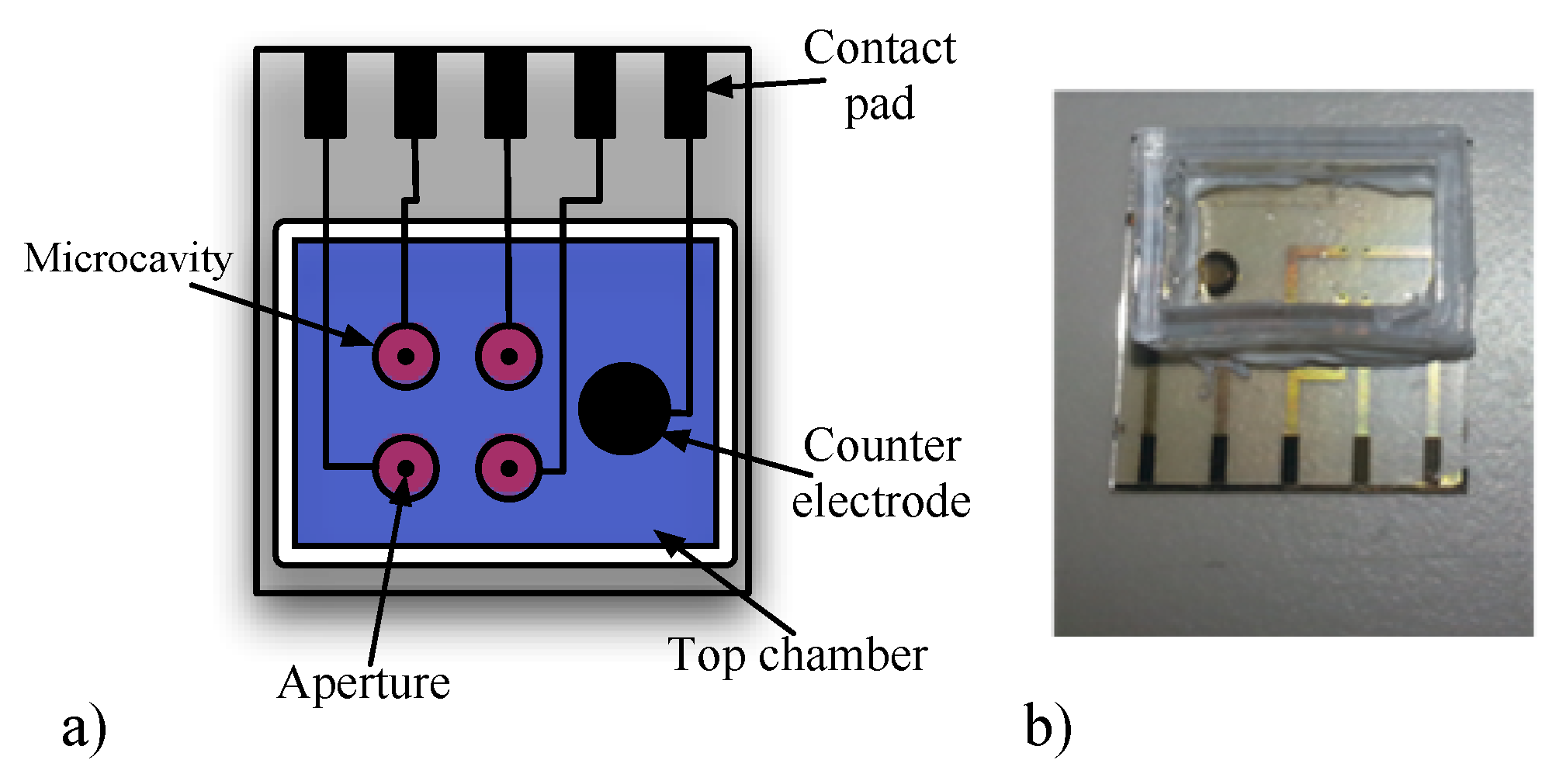
2.2. Microfluidic Device
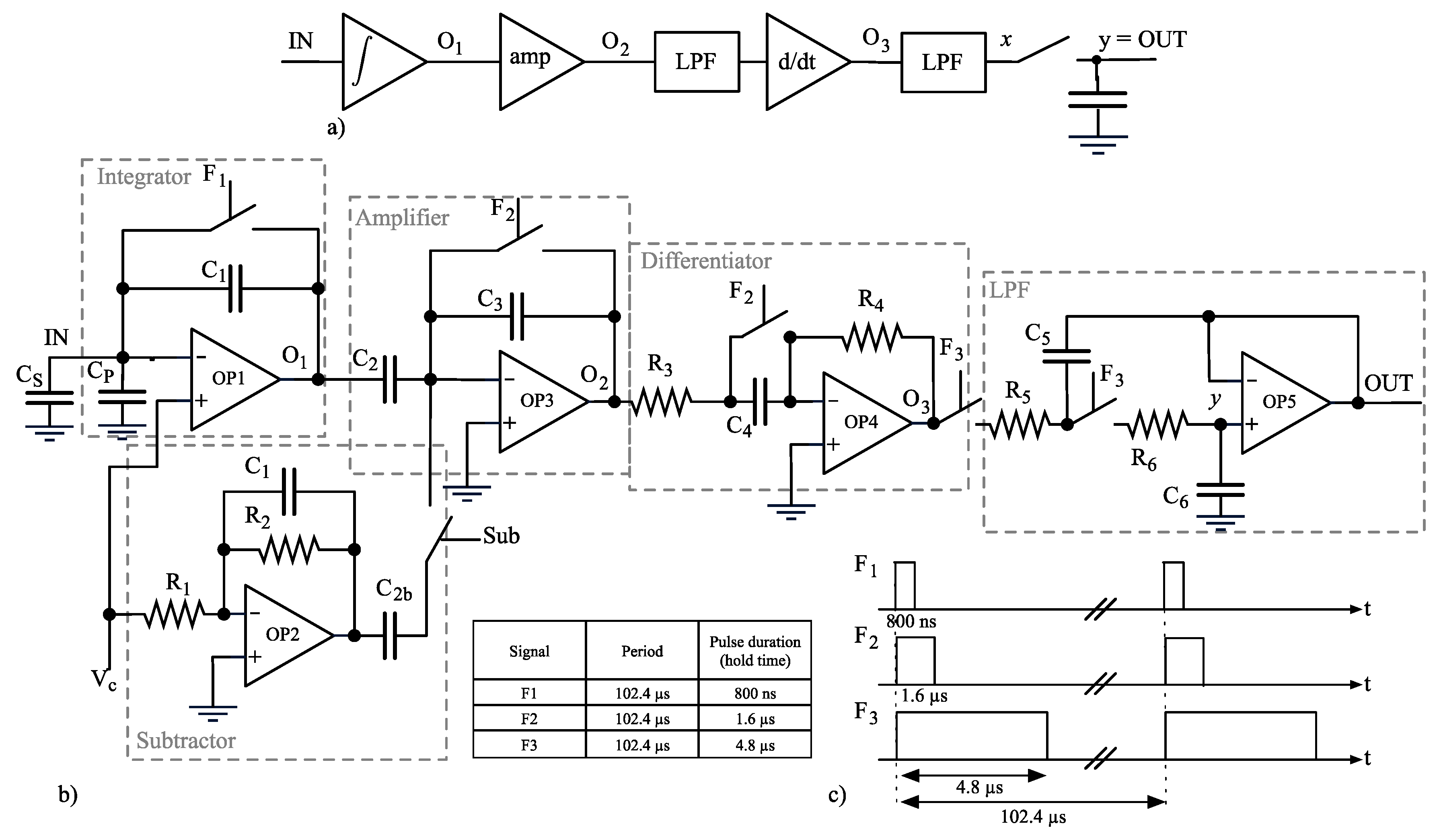
2.3. Sensing Frontend Rationale
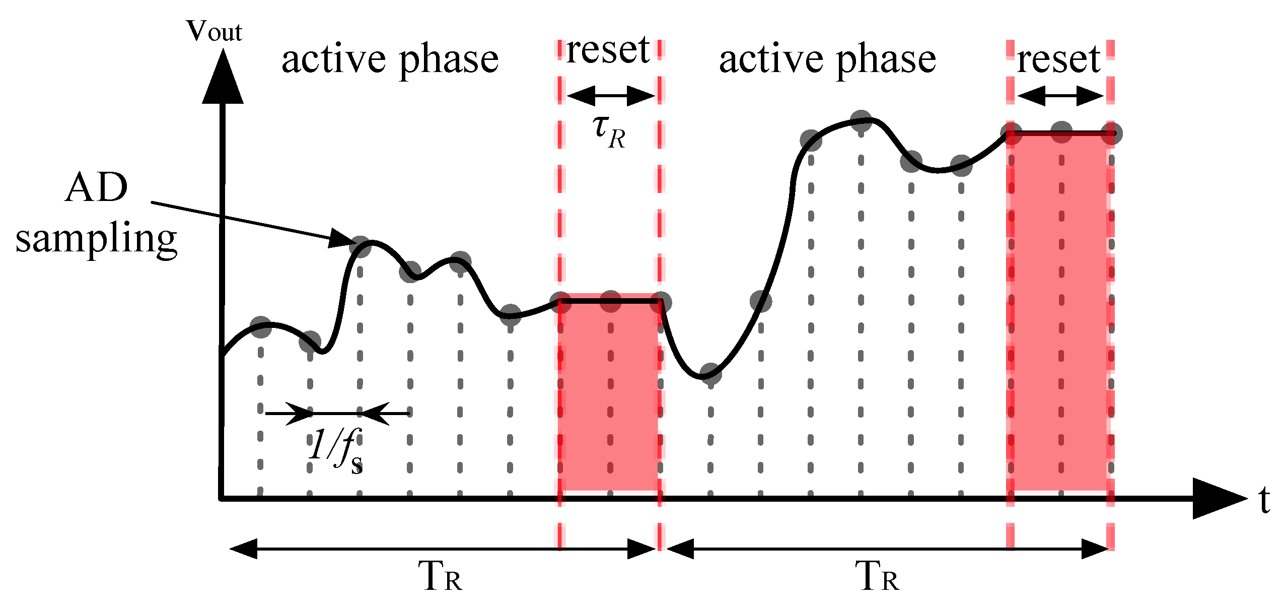
- Active phase. During this phase where Req is the equivalent trans-resistance of the amplifier, which is given by:
- Reset phase. During this phase the output voltage is kept constant while the rest of the circuit reset.
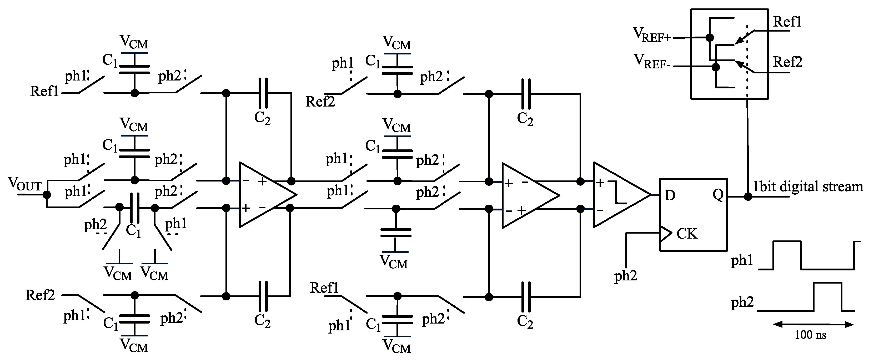
2.4. ADC
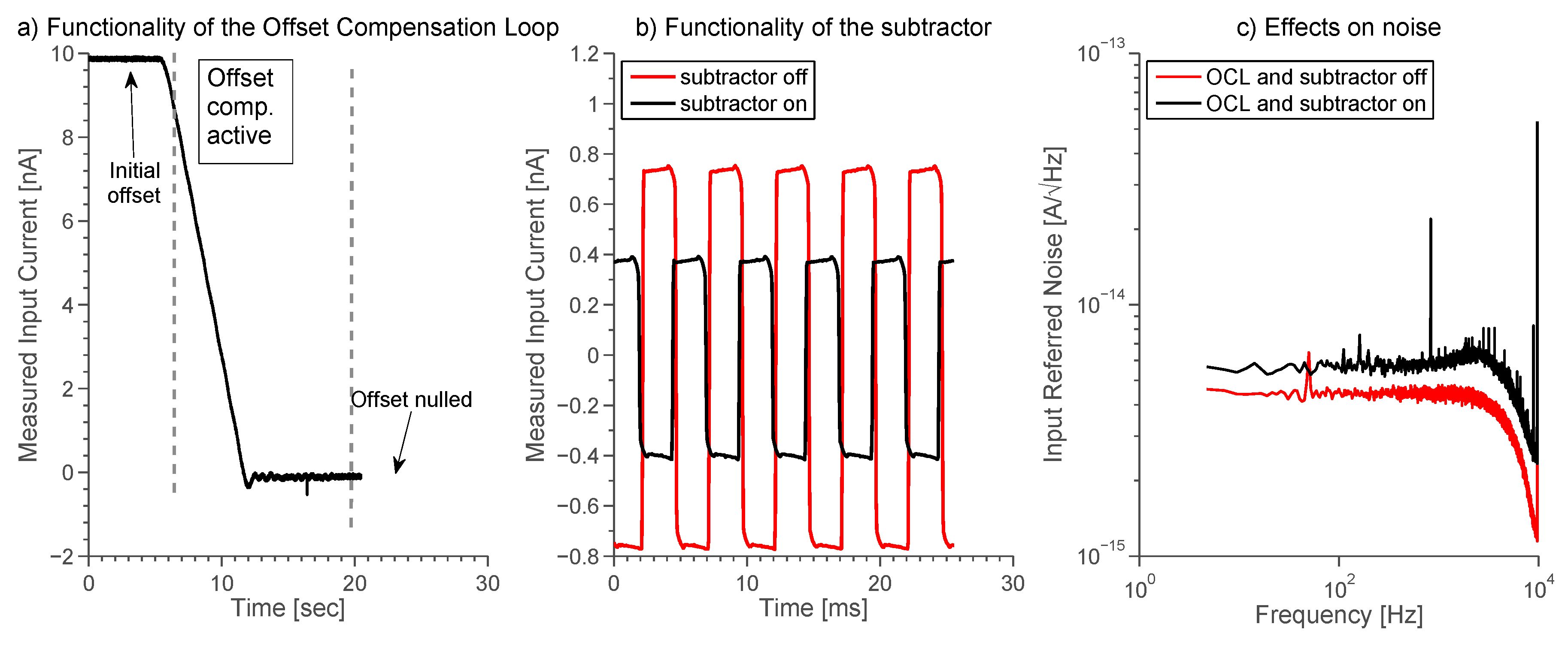
2.5. Stimulus Generation and Offset Compensation
2.6. Subtractor
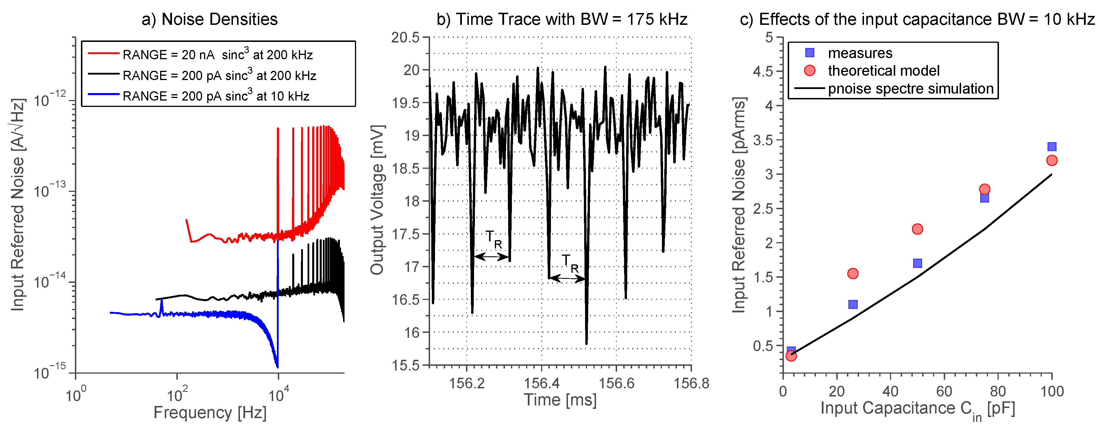
2.7. Noise Analysis
- all the stages prior to the sampling are treated as linear time-invariant systems;
- node x takes into account low-pass filtering done by the Sallen-Key but not the sampling; there is not a direct correspondence of node x in the schematic diagram (Figure 5b).
- node OUT is renamed into y to get more compact equations.
- -
- The most direct method of reducing folding noise is lowering the USR, which defines how many times the noise folds back into the baseband. This can be easily done by lowering fp, but this directly affects the bandwidth of the system and the sampling error [14]. Moreover, if 1/fp becomes greater than the reset pulse duration τR then Equations (18) and (19) are no longer valid, since cross-correlation power computed from Equation (17) must be taken into consideration.
- -
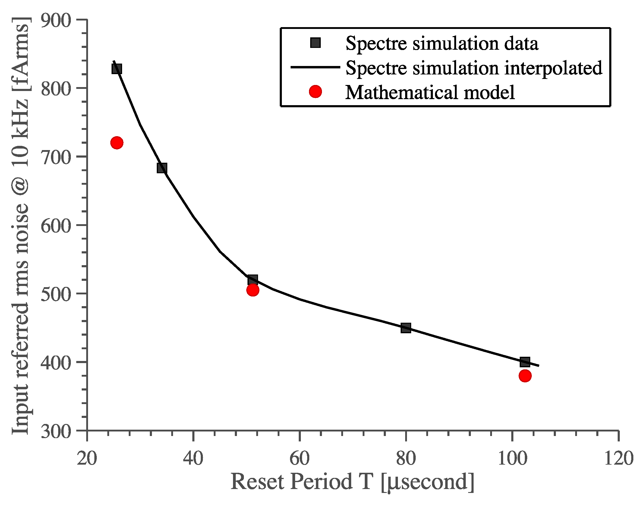
- Another important parameter is the period TR, which appears in both USR and pre-factor. It should be small to lower USR while it should be big to lower the pre-factor (τR/TR)2. Since TR is squared in the pre-factor term then it is better to make it as high as possible. This relation between noise and parameter TR is confirmed by periodic-steady-state noise (pss-noise) analysis and it is predicted by our mathematical model, see Figure 10.
- -
- Another way of reducing the folding noise is to keep Gx(f) as low as possible. This directly translates into using a low-noise OTA and lowering the input capacitance CIN as well as the feedback capacitance C1, creating a noise-bandwidth trade-off.
3. Experimental Results
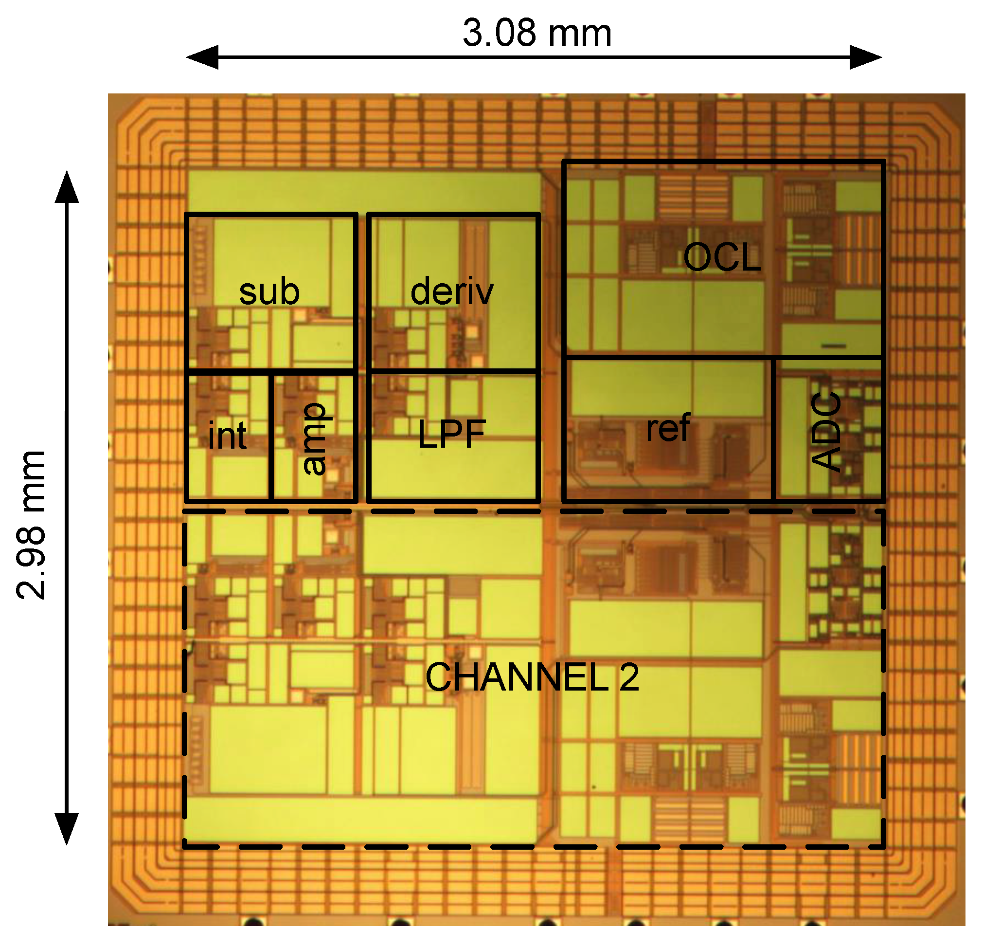
3.1. Implementation
3.2. Noise Measurements
3.3. Offset Compensation Loop and Subtractor
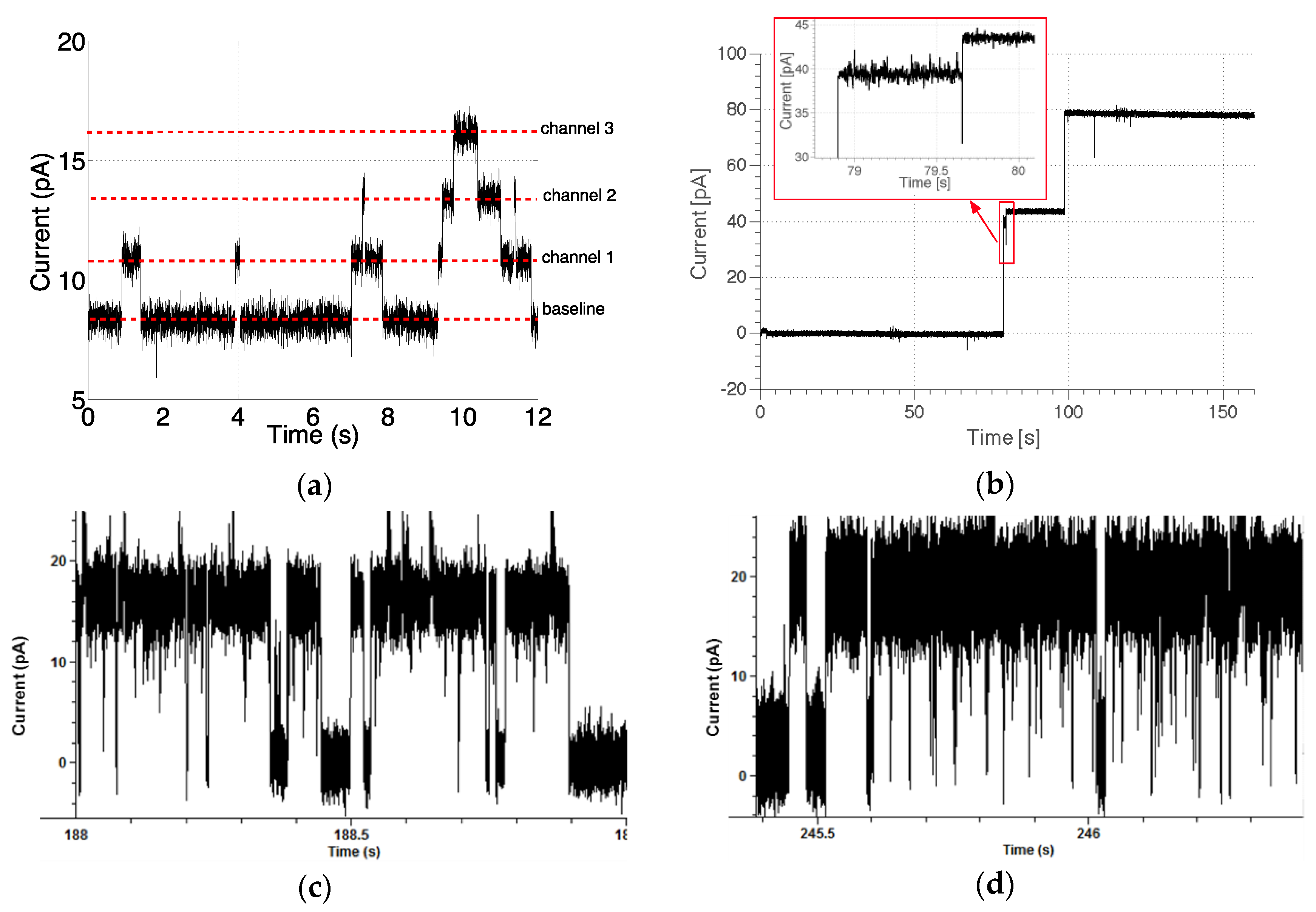
3.4. Ion Channel Recording
3.4.1. Gramicidin-A
3.4.2. α-Haemolysin
3.4.3. KcsA Potassium Channel
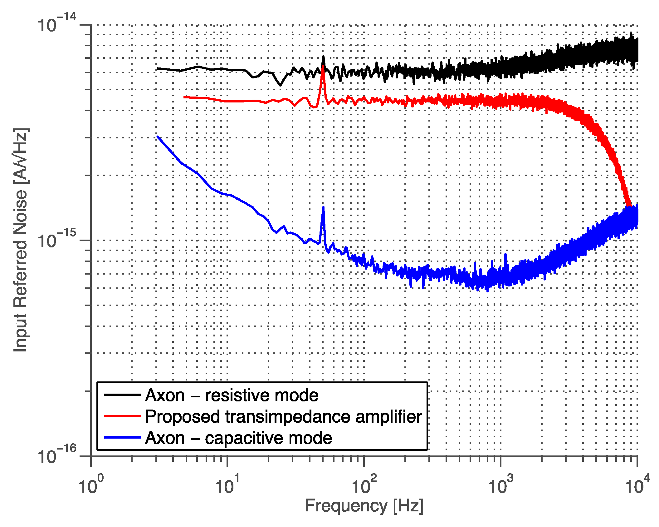
3.5. State-of-the-Art Comparison
4. Conclusions
Acknowledgments
Author Contributions
Conflicts of Interest
References
- Hille, B. Ion Channels of Excitable Membranes, 3rd ed.; Sinauer Associates: Sunderland, MA, USA, 2001. [Google Scholar]
- Bayley, H.; Cremer, P.S. Stochastic sensors inspired by biology. Nature 2001, 413, 226–230. [Google Scholar] [CrossRef] [PubMed]
- Sakmann, B.; Neher, E. Single-Channel Recording, 2nd ed.; Springer-Verlag: Berlin, Germany, 2009. [Google Scholar]
- Fertig, N.; Blick, R.H.; Behrends, J.C. Whole cell patch clamp recording performed on a planar glass chip. Biophys. J. 2002, 82, 3056–3062. [Google Scholar] [CrossRef]
- Tien, H.T. Bilayer Lipid Membranes (BLM): Theory and Practice; Dekker: New York, NY, USA, 1974. [Google Scholar]
- Suzuki, H.; Takeuchi, S. Microtechnologies for membrane protein studies. Anal. Bioanal. Chem. 2008, 391, 2695–2702. [Google Scholar] [CrossRef] [PubMed]
- Kreir, M.; Farre, C.; Beckler, M.; George, M.; Fertig, N. Rapid screening of membrane protein activity: Electrophysiological analysis of OmpF reconstituted in proteoliposomes. Lab Chip 2008, 8, 587–595. [Google Scholar] [CrossRef] [PubMed]
- Suzuki, H.; Le Pioufle, B.; Takeuchi, S. Ninety-six-well planar lipid bilayer chip for ion channel recording fabricated by hybrid stereolithography. Biomed. Microdevices 2009, 11, 17–22. [Google Scholar] [CrossRef] [PubMed]
- Zagnoni, M. Miniaturised technologies for the development of artificial lipid bilayer systems. Lab Chip 2012, 12, 1026–1039. [Google Scholar] [CrossRef] [PubMed]
- Rosenstein, J. The promise of nanopore technology: Nanopore DNA sequencing represents a fundamental change in the way that genomic information is read, with potentially big savings. IEEE Pulse 2014, 5, 52–54. [Google Scholar] [CrossRef] [PubMed]
- Thei, F.; Rossi, M.; Bennati, M.; Crescentini, M.; Lodesani, F.; Morgan, H.; Tartagni, M. Parallel Recording of Single Ion Channels: A Heterogeneous System Approach. IEEE Trans. Nanotechnol. 2010, 9, 295–302. [Google Scholar] [CrossRef]
- Saha, S.C.; Thei, F.; de Planque, M.R.R.; Morgan, H. Scalable micro-cavity bilayer lipid membrane arrays for parallel ion channel recording. Sens. Actuators B Chem. 2014, 199, 76–82. [Google Scholar] [CrossRef]
- Crescentini, M.; Thei, F.; Bennati, M.; Saha, S.; de Planque, M.R.R.; Morgan, H.; Tartagni, M. A Distributed Amplifier System for Bilayer Lipid Membrane (BLM) Arrays With Noise and Individual Offset Cancellation. IEEE Trans. Biomed. Circuits Syst. 2015, 9, 334–344. [Google Scholar] [CrossRef] [PubMed]
- Crescentini, M.; Bennati, M.; Carminati, M.; Tartagni, M. Noise Limits of CMOS Current Interfaces for Biosensors: A Review. IEEE Trans. Biomed. Circuits Syst. 2013, 8, 278–292. [Google Scholar] [CrossRef] [PubMed]
- Kim, D.; Goldstein, B.; Tang, W.; Sigworth, F.J.; Culurciello, E. Noise Analysis and Performance Comparison of Low Current Measurement Systems for Biomedical Applications. IEEE Trans. Biomed. Circuits Syst. 2013, 7, 52–62. [Google Scholar]
- LeMasurier, M.; Heginbotham, L.; Miller, C. KcsA: It’s a potassium channel. J. Gen. Physiol. 2001, 118, 303–314. [Google Scholar] [CrossRef] [PubMed]
- Goldstein, B.; Kim, D.; Magoch, M.; Astier, Y.; Culurciello, E. CMOS low current measurement system for nanopore sensing applications. In Proceedings of the IEEE Biomedical Circuits and Systems Conference (BioCAS), San Diego, CA, USA, 10–12 November 2011; pp. 265–268.
- Axon Instruments, Inc. The Axon Guide for Electrophysiology & Biophysics Laboratory Techniques; Axon Instruments, Inc.: Foster City, CA, USA, 1993. [Google Scholar]
- Hsu, C.-L.; Venkatesh, A.G.; Jiang, H.; Hall, D.A. A hybrid semi-digital transimpedance amplifier for nanopore-based DNA sequencing. In Proceedings of the IEEE Biomedical Circuits and Systems Conference (BioCAS), Lausanne, Switzerland, 22–24 October 2014; pp. 452–455.
- Jafari, H.M.; Genov, R. Chopper-Stabilized Bidirectional Current Acquisition Circuits for Electrochemical Amperometric Biosensors. IEEE Trans. Circuits Syst. I Regul. Pap. 2013, 60, 1149–1157. [Google Scholar] [CrossRef]
- Rosenstein, J.; Wanunu, M.; Merchant, C.A.; Drndic, M.; Shepard, K.L. Integrated nanopore sensing platform with sub-microsecond temporal resolution. Nat. Methods 2012, 9, 487–492. [Google Scholar] [CrossRef] [PubMed]
- Schreier, R.; Temes, G.C. Understanding Delta-Sigma Data Converters; Wiley-IEEE Press: Piscataway, NJ, USA, 2004. [Google Scholar]
- Crescentini, M.; Rossi, M.; Bennati, M.; Thei, F.; Baschirotto, A.; Tartagni, M. A nanosensor interface based on delta-sigma Arrays. In Proceedings of the 3rd International Workshop on Advances in Sensors and Interfaces (IWASI), Trani, Italy, 25–26 June 2009; pp. 163–167.
- Shinwari, M.W.; Zhitomirsky, D.; Deen, I.A.; Selvaganapathy, P.R.; Deen, M.J.; Landheer, D. Microfabricated reference electrodes and their biosensing applications. Sensors 2010, 10, 1679–1715. [Google Scholar] [CrossRef] [PubMed]
- Matsumoto, T.; Ohashi, A.; Ito, N. Development of a micro-planar Ag/AgCl quasi-reference electrode with long-term stability for an amperometric glucose sensor. Anal. Chim. Acta 2002, 462, 253–259. [Google Scholar] [CrossRef]
- Polk, B.J.; Stelzenmuller, A.; Mijares, G.; MacCrehan, W.; Gaitan, M. Ag/AgCl microelectrodes with improved stability for microfluidics. Sens. Actuators B Chem. 2006, 114, 239–247. [Google Scholar] [CrossRef]
- Thei, F.; Rossi, M.; Bennati, M.; Crescentini, M.; Tartagni, M. An automatic offset correction platform for high-throughput ion-channel electrophysiology. Procedia Eng. 2010, 5, 816–819. [Google Scholar] [CrossRef]
- Enz, C.; Temes, G. Circuit techniques for reducing the effects of op-amp imperfections: Autozeroing, correlated double sampling, and chopper stabilization. Proc. IEEE 1996, 84, 1584–1614. [Google Scholar] [CrossRef]
- Fischer, J.H. Noise sources and calculation techniques for switched capacitor filters. IEEE J. Solid-State Circuits 1982, 17, 742–752. [Google Scholar] [CrossRef]
- Phillips, J.; Kundert, K. An Introduction to Cyclostationary Noise: Noise in mixers, oscillators, samplers, and logic. In Proceedings of the IEEE 2000 Custom Integrated Circuits Conference (CICC), Orlando, FL, USA, 21 May 2000; pp. 431–438.
- Gardner, W.A. Introduction to Random Processes with Applications to Signal & Systems, 2nd ed.; McGraw-Hill: New York, NY, USA, 1990. [Google Scholar]
- Proakis, J.G. Digital Communications; McGraw-Hill: New York, NY, USA, 2000. [Google Scholar]
- Woolley, G.A.; Wallace, B.A. Model ion channels: Gramicidin and alamethicin. J. Membr. Biol. 1992, 129, 109–136. [Google Scholar] [PubMed]
- Allen, T.W.; Andersen, O.S.; Roux, B. Energetics of ion conduction through the gramicidin channel. Proc. Natl. Acad. Sci. USA 2004, 101, 117–122. [Google Scholar] [CrossRef] [PubMed]
- Hromada, L.P.; Nablo, J.P.; Kasianowicz, J.J.; Gaitan, M.A.; DeVoe, D.L. Single molecule measurements within individually membrane- bound ion channels using a polymer-based bilayer lipid membrane chip. Lab Chip 2008, 8, 602–608. [Google Scholar] [CrossRef] [PubMed]
- Kawano, R.; Osaki, T.; Sasak, H.; Takinoue, M.; Yoshizawa, S.; Takeuchi, S. Rapid detection of a cocaine-binding aptamer using biological nanopores on a chip. Am. Chem. Soc. J. 2011, 133, 8474–8477. [Google Scholar] [CrossRef] [PubMed]
- Ferrari, G.; Farina, M.; Guagliardo, F.; Carminati, M.; Sampietro, M. Ultra-low-noise CMOS current preamplifier from DC to 1 MHz. Electron. Lett. 2009, 45, 1278–1280. [Google Scholar] [CrossRef]
- Ferrari, G.; Gozzini, F.; Molari, A.; Sampietro, M. Transimpedance amplifier for high sensitivity current measurements on nanodevices. IEEE J. Solid-State Circuits 2009, 44, 1609–1616. [Google Scholar] [CrossRef]
- Goldstein, B.; Kim, D.; Rottigni, A.; Xu, J.; Vanderlick, T.K.; Culurciello, E. CMOS low current measurement system for biomedical applications. In Proceedings of the IEEE International Symposium of Circuits and Systems (ISCAS), Rio de Janeiro, Brazil, 15–18 May 2011; pp. 1017–1020.
- Dai, S.; Rosenstein, J.K. A dual-mode low-noise nanosensor front-end with 155-dB dynamic range. In Proceedings of the IEEE Biomedical Circuits and Systems Conference (BioCAS), Atlanta, GA, USA, 22–24 October 2015; pp. 1–4.


| Component | C1 | C2 | C3 | C4 | R4 | R3 | TR | τR |
|---|---|---|---|---|---|---|---|---|
| Value | 1 pF | 22 pF | 1 pF | 102.4 pF | 1 MΩ | 2.2 kΩ | 102.4 μs | 4.8 μs |
| Theory (18) | Simulation | Measure | |
|---|---|---|---|
| RMS NOISE at 10 kHz | 380 fA | 400 fA | 420 fA |
| Conditions | CIN = CP = 3 pF | CIN = CP = 3 pF | Open-input |
| Paper | Noise floor @ Room Temperature | Embedded ADC | Analog Power Consumption | Digital Power Consumption | Input Capacitance for Characterization of Noise Floor | Operating Bandwidth [kHz] | Gain [GΩ] | Technology Node |
|---|---|---|---|---|---|---|---|---|
| [21] | 12 fA/√Hz | NO | - | - | - | 10.000 | <1 | CMOS 0.13 μm |
| [20] | 2 fA/√Hz | NO | 3 μW | - | - | 6 | >1 | CMOS 0.13 μm |
| [37] | 0.5 fA/√Hz | NO | - | - | 1 pF | 1000 | *1 | - |
| [39] | 6 fA/√Hz | NO | 1.5 mW | - | 7 pF | 50 | - | CMOS 0.5 μm |
| [38] | 4 fA/√Hz | NO | 45 mW | - | 800 fF | 10,000 | 0.06 | CMOS 0.35 μm |
| [40] | 11.6 fA/√Hz | NO | 5.22 mW | - | - | 1400 | 0.01 | CMOS 0.18 μm |
| [13] | 3 fA/√Hz@B = 625 Hz 12 fA/√Hz @B = 10 kHz | YES | 20 mW | 20 mW | 3 pF | 10 | 2.25 | CMOS 0.35 μm |
| This work | 4 fA/√Hz*2 @B = 7.5 kHz 6 fA/√Hz *2 @B = 175 kHz | YES | 21 mW | 20 mW | 3 pF | 100 | 2.25 | CMOS 0.35 μm |
© 2016 by the authors; licensee MDPI, Basel, Switzerland. This article is an open access article distributed under the terms and conditions of the Creative Commons Attribution (CC-BY) license (http://creativecommons.org/licenses/by/4.0/).
Share and Cite
Crescentini, M.; Bennati, M.; Saha, S.C.; Ivica, J.; De Planque, M.; Morgan, H.; Tartagni, M. A Low-Noise Transimpedance Amplifier for BLM-Based Ion Channel Recording. Sensors 2016, 16, 709. https://doi.org/10.3390/s16050709
Crescentini M, Bennati M, Saha SC, Ivica J, De Planque M, Morgan H, Tartagni M. A Low-Noise Transimpedance Amplifier for BLM-Based Ion Channel Recording. Sensors. 2016; 16(5):709. https://doi.org/10.3390/s16050709
Chicago/Turabian StyleCrescentini, Marco, Marco Bennati, Shimul Chandra Saha, Josip Ivica, Maurits De Planque, Hywel Morgan, and Marco Tartagni. 2016. "A Low-Noise Transimpedance Amplifier for BLM-Based Ion Channel Recording" Sensors 16, no. 5: 709. https://doi.org/10.3390/s16050709
APA StyleCrescentini, M., Bennati, M., Saha, S. C., Ivica, J., De Planque, M., Morgan, H., & Tartagni, M. (2016). A Low-Noise Transimpedance Amplifier for BLM-Based Ion Channel Recording. Sensors, 16(5), 709. https://doi.org/10.3390/s16050709