1. Introduction
Resistive sensor arrays are important for tactile sensing [
1,
2,
3,
4,
5,
6,
7,
8], infrared sensing [
9,
10], light sensing [
11],
etc. For limited space in sensitive areas, many resistive sensor arrays used in robotic applications are connected with their test circuits with different length cables. Fernando
et al. [
1] designed a 16 × 9 force sensor patch with its test cable’s length more than 55 mm to cover large distances within robots and machines for interacting with human beings. Speeter [
2] reported a flexible sensing system with its test cable’s length more than 60 mm and achieved a sampling rate of more than 60 Hz in scanning 16 × 16 resistive taxels. Fernando
et al. [
3] realized and compared three circuits of networked piezoresistive sensor arrays with test cable length longer than 70 mm based on standard microcontrollers, programmable systems on chip, and field programmable gate arrays. Yang
et al. [
4] designed a 32 × 32 flexible array with a test cable length longer than 70 mm using PI-copper films within a 160 mm × 160 mm temperature and tactile sensing area, which could be used to recognize large objects of different shapes. Zhang
et al. [
5] reported a 3 × 3 thin tactile force sensor array with its test cable length longer than 95 mm based on conductive rubber. Castellanos-Ramos
et al. [
6] reported a 16 × 16 tactile sensor array with its test cable length greater than 100 mm based on conductive polymers with screen-printing technology. Kim
et al. [
7] reported a new concept of a flexible tactile sensor array with more length capable of sensing contact force and position with high performance and high spatial resolution. Lazzarini
et al. [
8] reported a 16 × 16 tactile sensor array for practical applications requiring manipulation with its test cable’s length of 500 mm. Saxena
et al. designed a 16 × 16 bolometer array of IR detectors [
9,
10] and a 16 × 16 imaging array of light-dependent resistors [
11]. With longer flexible test cables, the resistive sensor array modules are more flexible for robotic operations and easier to be connected with their test circuits.
In connected cables with fewer wires (
M +
N wires for a
M ×
N resistive array), sensor modules of networked resistive arrays in shared row-column fashion were connected with their test circuits [
11]. With equal length and the same material, wires of long cables had similar wire resistances which increased with the increase of cables’ length. Between the plugs of the connected cables and the sockets of the test circuits, there existed contacted resistances which varied in the range from 0 ohms to several ohms with the change of the contacted conditions caused by mechanical vibration and time variation. As for the voltage feedback circuits of the resistive networked sensor arrays in shared row-column fashion, the voltage differences between the circuits’ test ports and the sensor modules’ ports of the same connected wires were caused by the similar wire resistances and the different contacted resistances. Thus, the ideal feedback conditions in the voltage feedback circuits of the 2-D networked resistive sensor arrays were destroyed and crosstalk caused by the test cables existed. As such, good cable crosstalk suppression methods should be further studied.
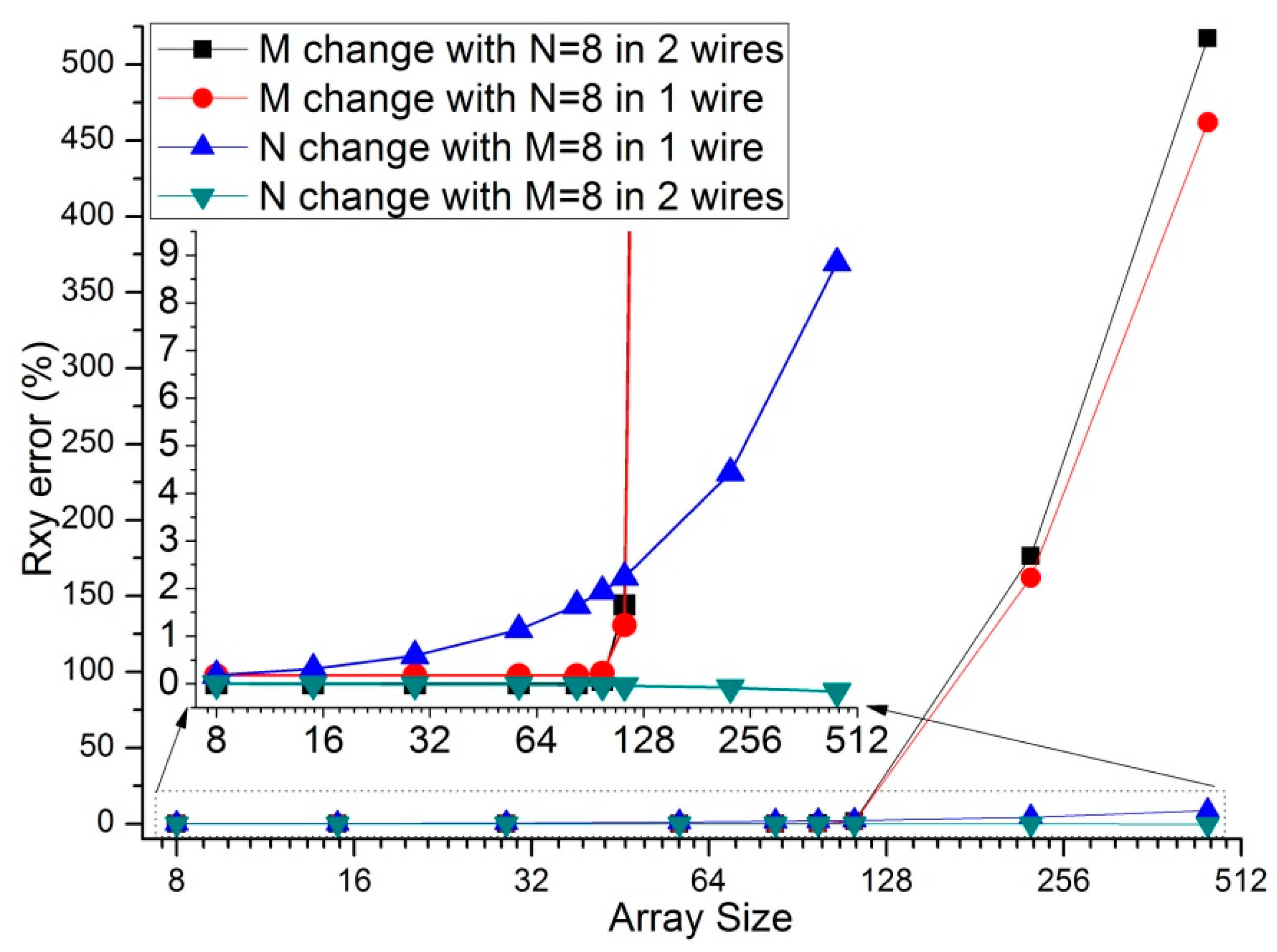
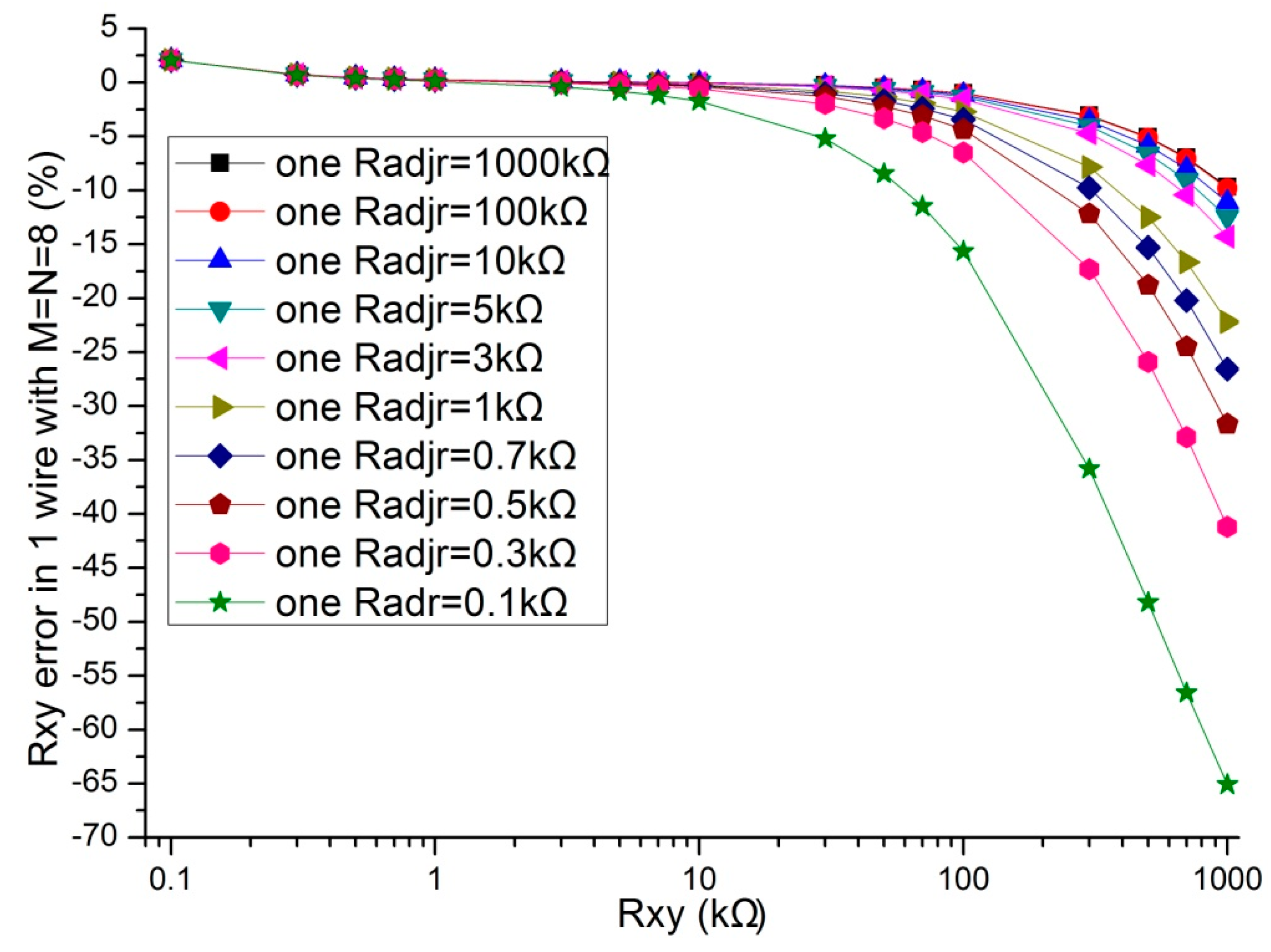
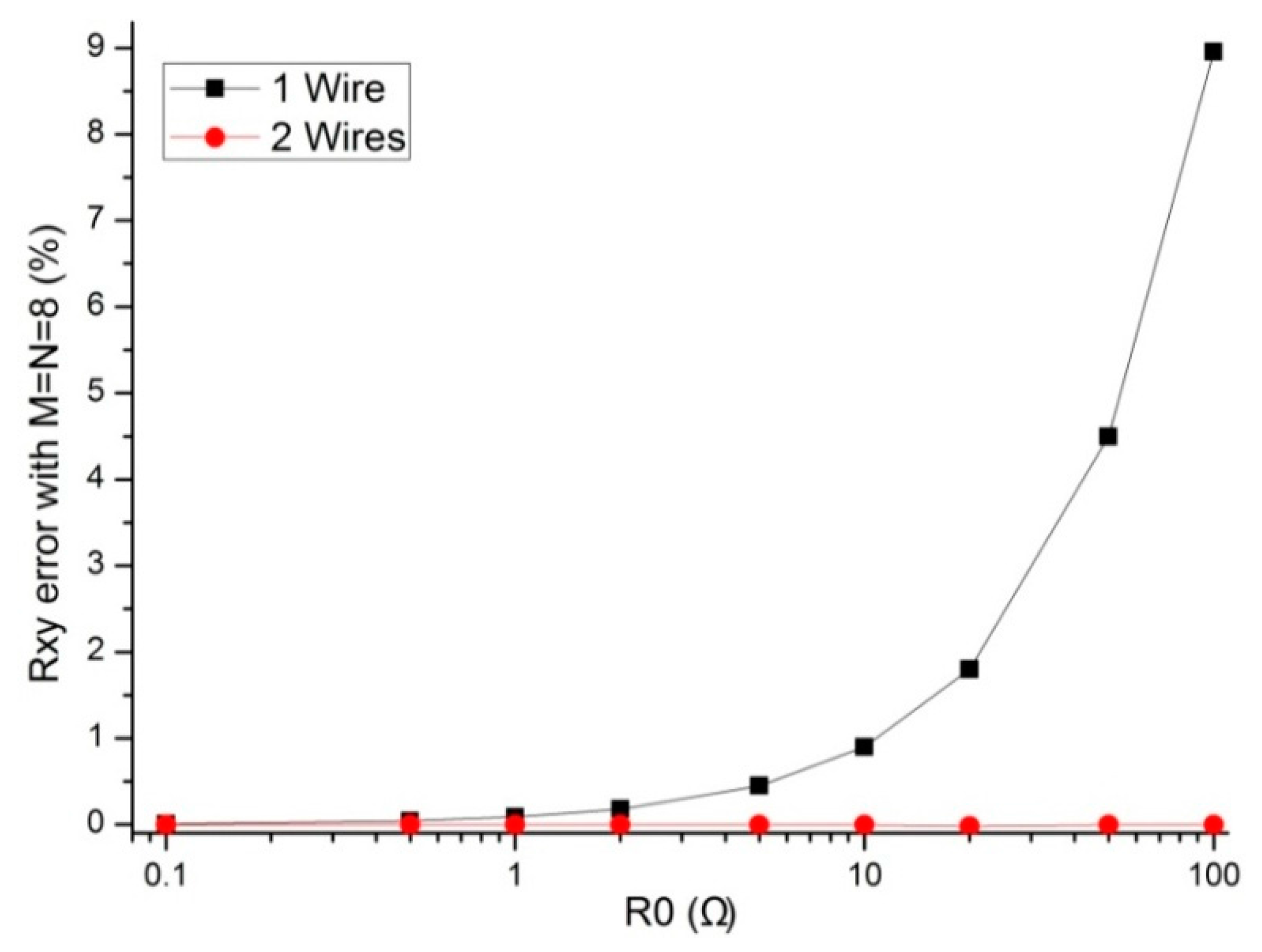
For this purpose, we present a novel cable crosstalk suppression method with less cost for the 2-D networked resistive sensor arrays in the row-column fashion. This paper begins with an overview of the application fields of the 2-D networked resistive sensor arrays. Secondly, a novel cable crosstalk suppression method will be proposed and its equivalent resistance expression of the element being tested will be analytically derived. Followed, experiments will be implemented to evaluate this method with different parameters such as the wire resistances and contacted resistances of the cables, the array size, the measurement range of the EBT, and the adjacent elements’ resistances of 2-D networked resistive sensor arrays. Finally, the results of experiments will be analyzed and conclusions for the method will be given.
2. Principle Analysis
With the row-column fashion, few wires were use in the 2-D networked resistive circuits. However, these circuits suffered from the crosstalk for parasitic parallel paths in the 2-D networked resistive sensor arrays, and some theoretical analyses had been implemented for suppressing it. Fernando
et al. [
1,
3,
4,
5,
6,
7,
8,
12,
13,
14] suppressed the crosstalk caused by the adjacent elements and the multiplexers with larger number of op-amps using virtual ground technique. With the Improved Isolated Drive Feedback Circuit (IIDFC) [
15], Wu
et al. depressed the crosstalk error caused by the adjacent column elements. With the Improved Isolated Drive Feedback Circuit with Compensation (IIDFCC) [
16], Wu
et al. reduced the influence on the EBT caused by parasitic parallel paths for the multiplexers’ channel resistor and the adjacent elements. In these methods, the measurement accuracy of the EBT still suffered from the interferences of cables’ parameters, such as wire resistances and contacted resistances. Liu
et al. [
17] defined the voltage feedback method including the voltage feedback non-scanned-electrode (VF-NSE) method, the voltage feedback non-scanned-sampling-electrode (VF-NSSE) method, and the voltage feedback non-scanned-driving-electrode (VF-NSDE) method. Wu
et al. [
18] proposed a general voltage feedback circuit model for the two-dimensional networked resistive sensor array.
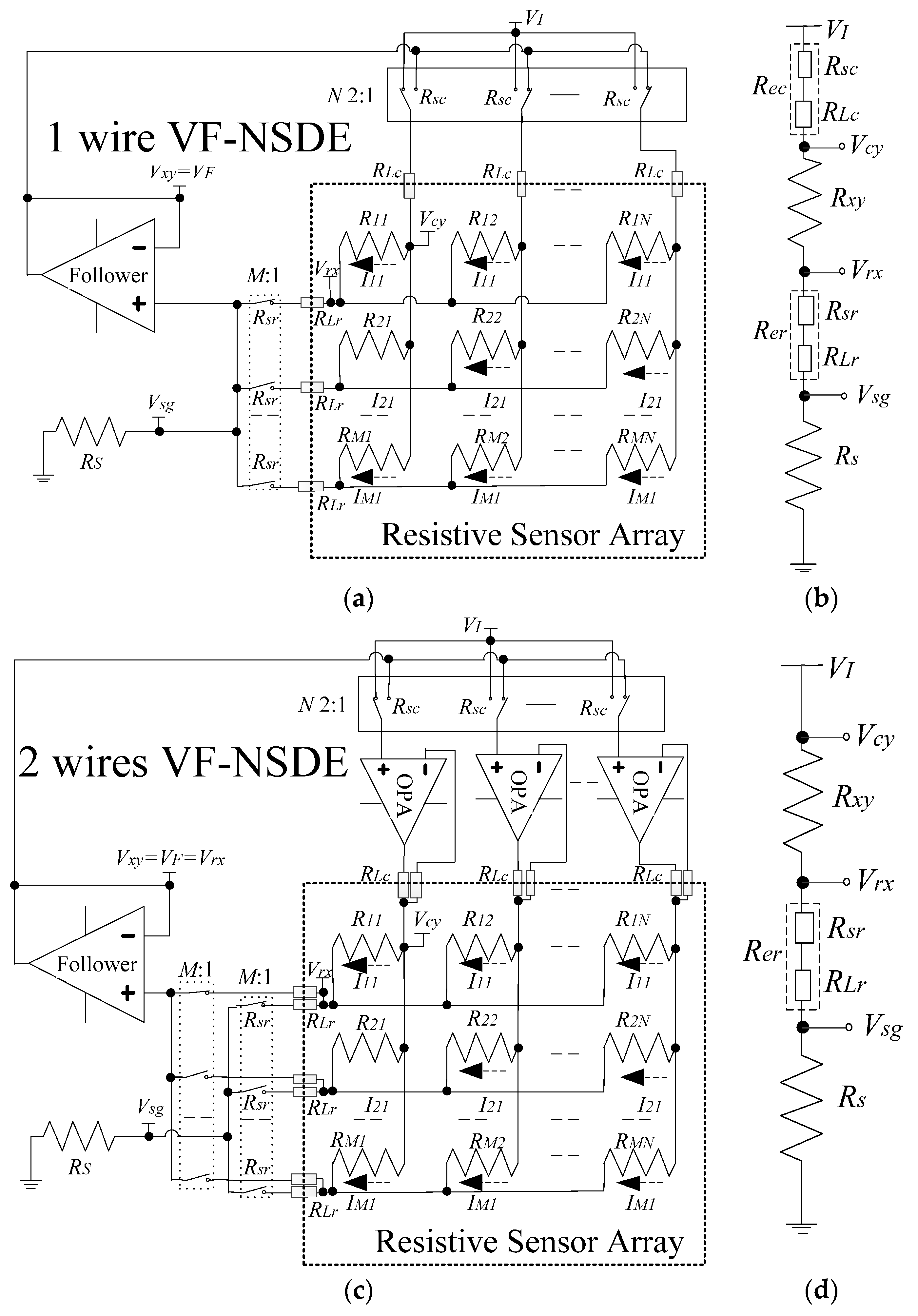
In this analysis, a VF-NSDE circuit was taken as the example. A traditional VF-NSDE circuit of a resistive networked sensor array in a shared row-column fashion is shown as Circuit A in
Figure 1a. In Circuit A,
R11 in the
M ×
N resistive array was the element being tested (EBT); only one connected wire was used for every row line and every column line between the array and the circuit; only one equal current
M:1 multiplexer was used between the sampling resistor (
Rs) and the row lines of the sensor module. On the column lines of the circuit, 2:1 multiplexers had multiplexer switch resistances (
Rscs); column wires had column resistances (
RLcs) including column wire resistances and contacted resistances. On row lines of the circuit, the equal current
M:1 multiplexers had multiplexer switch resistances (
Rsrs); row wires had row resistances (
RLrs) including row wire resistances and contacted resistances. Thus, the Circuit A had one voltage feedback op-amp,
N 2:1 multiplexers, and
M +
N wires.
Under an ideal condition, all
Rscs and all
RLcs were omitted. Thus, the voltage (
Vcy) on the column line of EBT was equal to the set voltage (
VI), and the voltages on non-scanned column lines were equal to the feedback voltage (
VF). At the same time, all
Rsrs and all
RLrs were omitted. Thus, the voltage (
Vsg) on
Rs was equal to the voltage (
Vrx) on the row line of EBT. Under the effect of the ideal op-amp,
VF followed the change of
Vsg. Thus,
VF,
Vrx, and
Vsg were equal. As the voltages on non-scanned column lines were equal to
Vrx, the currents on the adjacent row elements of EBT were equal to zero. At the same time, the current on the non-inverting input of the ideal op-amp was omitted for its infinite input impedance, the current (
Ixy) on the EBT was equal to the current (
Is =
Vsg/
Rs = (
VI −
Vrx)/
Rxy = (
VI −
Vsg)/
Rxy) on
Rs. As
VI and
Rs were known,
Vsg =
VF could be measured by ADC, so the equivalent resistance value (
Rxy) of the EBT in the Circuit A could be calculated with Equation (1):
However, under real conditions, as shown in
Figure 1b,
Vcy was not equal to
VI for
Rsc and
RLc, and
Vsg was not equal to
Vrx for
Rsr and
RLr. The ideal feedback condition was destroyed by the row wires and the column wires, so extra measurement errors of the EBT occurred. For suppression crosstalk of the cables in the 2-D networked resistive arrays, we proposed a two-wire voltage feedback method as shown in
Figure 1c.
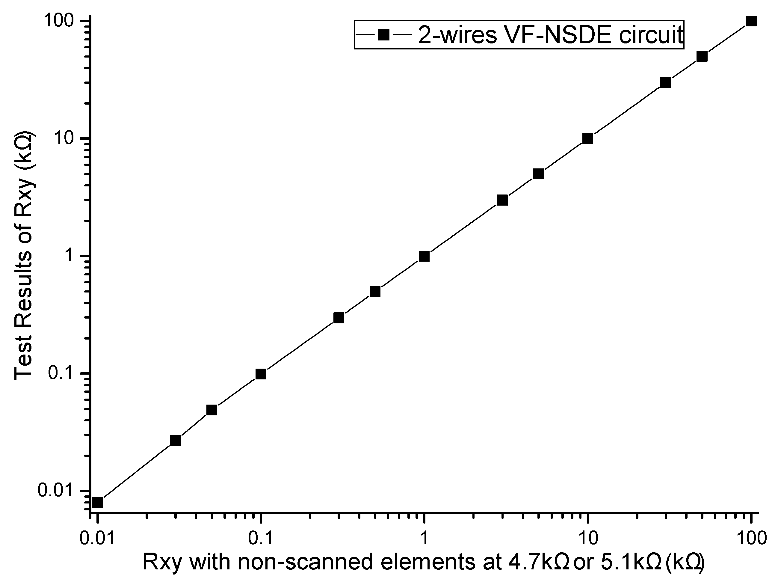
In the Circuit C, we used two wires for every row line and every column line between the sensor module and the test circuit; also we used one column driving op-amp for every column line and one equipotential M:1 multiplexer between the row lines and the voltage feedback op-amp. Thus, Circuit C had one voltage feedback op-amp, N column driving op-amps, N 2:1 multiplexers, two M:1 multiplexers, and 2(M + N) wires.
Every column line in the sensor module was connected with the output of its column driving op-amp by one driving wire and it was also connected with the inverting input of its column driving op-amp by one driving sampling wire. The non-inverting input of every column driving op-amp was connected with the common port of its column 2:1 multiplexer, thus every non-inverting input was connected with VI or VF. The non-inverting input of the EBT’s column driving op-amp was connected with VI while the non-inverting inputs of other column driving op-amps were connected with VF.
As the input impedance of every column driving op-amp was much bigger than its Rsc, the effect of all Rscs could be omitted. Thus, the voltage on the non-inverting input of its column driving op-amp was equal to the input voltage (VI or VF) on its 2:1 multiplexer. If the column driving op-amps had sufficient driving ability, the voltage on every column line followed the change of the voltage on the non-inverting input of its column driving op-amp. So Vcy was equal to VI, and the voltages on non-scanned column lines were equal to VF. Thus the crosstalk effect of RLcs and Rscs were suppressed.
By one equal current wire, every row line in the sensor module was connected with one channel of the equal current M:1 multiplexer with its common port connected with Rs. In the equal current M:1 multiplexer, only the row line of EBT was gated and all other non-scanned lines were suspended. So, only the row line of the EBT was connected with Rs.
By one equipotential wire, every row line in the sensor module was also connected with one channel of the equipotential M:1 multiplexer with its common port connected with the non-inverting input of the voltage feedback op-amp. In the equipotential M:1 multiplexer, only the row line of EBT was gated and all other non-scanned lines were suspended. Only the row line of the EBT was connected with the non-inverting input of the voltage feedback op-amp. From the EBT’s column driving op-amp, the test current firstly flowed through the EBT, then it flowed through the equal current wire, followed it flowed through the equal current M:1 multiplexer, finally it flowed through Rs to ground.
As the input impedance of the voltage feedback op-amp was much larger than its series resistances including the switch-on resistance of the equipotential M:1 multiplexer, and the wire resistance and the contacted resistance of the equipotential, the voltage on the non-inverting input of the voltage feedback op-amp was equal to the voltage (Vrx) of the EBT’s row line. Under the effect of the voltage feedback op-amp, VF followed the change of Vrx. Thus, VF was equal to Vrx. As the input impedance of the voltage feedback op-amp was much larger than its parallel resistances, such as Rs, Rsr, and RLr, the leak current on the non-inverting input of the voltage feedback op-amp could be omitted, as the voltage on every non-scanned column line was equal to VF, which was equal to Vrx. Thus, the currents on the EBT’s (N − 1) row adjacent elements were zero. The current (Is) on Rs was equal to the current (Ixy) on the EBT. The current with equal value also flowed through Rsr and RLr. As Rs was known and Is was equal to Ixy, we know Ixy if the voltage (Vsg) on Rs and the voltage (Vxy = Vcy − Vrx = VI − Vrx) on the EBT were known. Then we could get Rxy of the EBT.
However,
Vsg was not equal to
VF =
Vrx for
Rer (
Figure 1d) which was the crosstalk caused by the row wire. Thus, extra measurement error of the EBT was created. From the above discussion, we could know that the currents on
Rxy,
Rs, and
Rer had equal values. We could use Equation (2) to calculate
Rxy in the Circuit C. We could find that no
Rer existed in Equation (2). As
VI and
Rs were known,
Vsg and
VF could be measured by ADC, so the equivalent resistance value (
Rxy) of the EBT in the Circuit C could be calculated with Equation (2). Thus, the crosstalk caused by the row wires was suppressed.
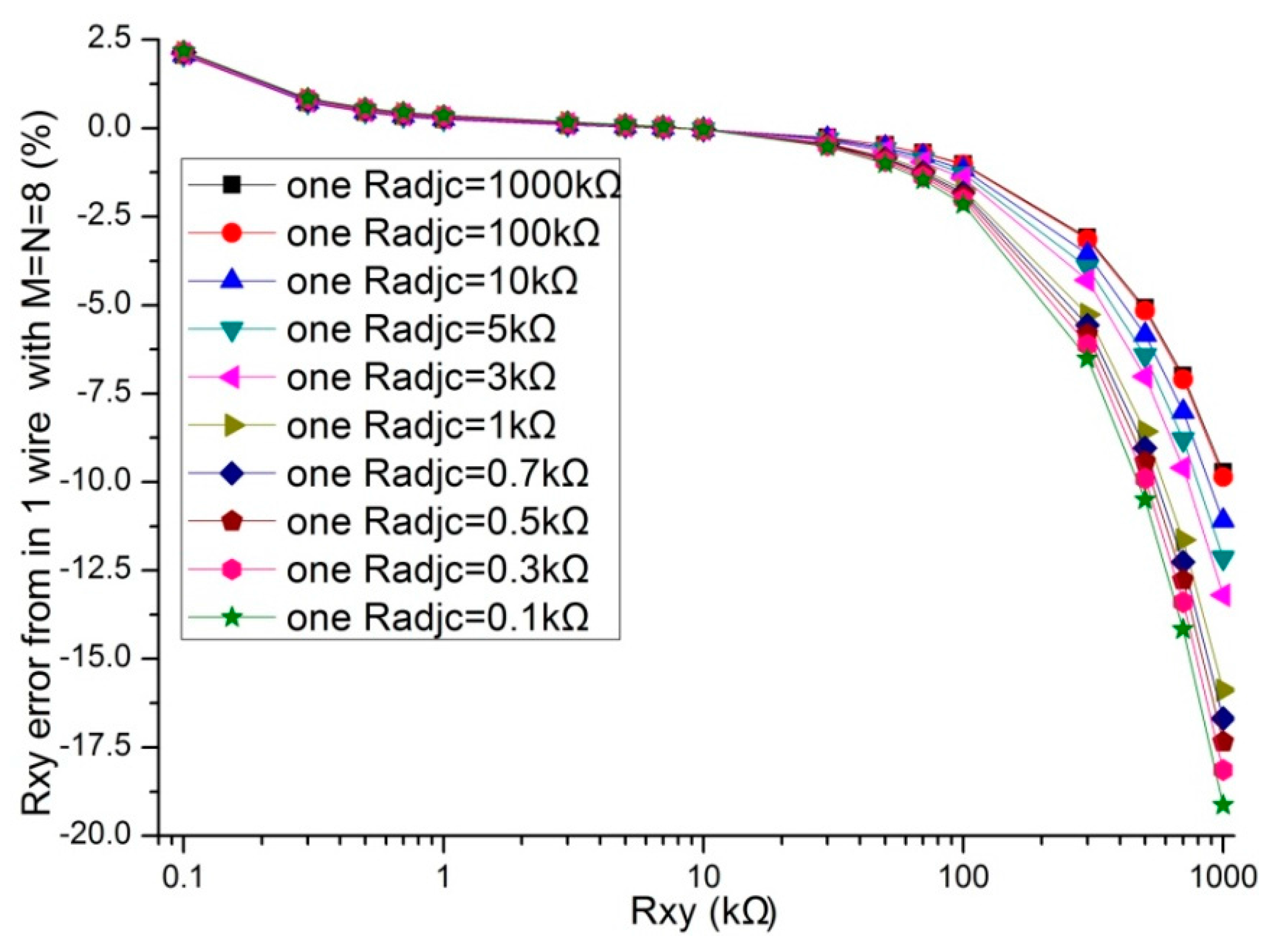
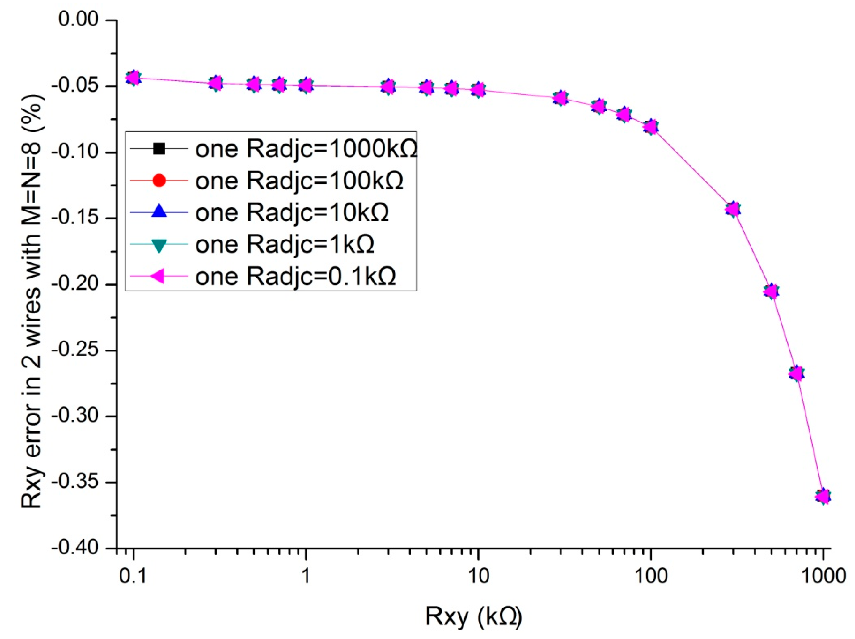
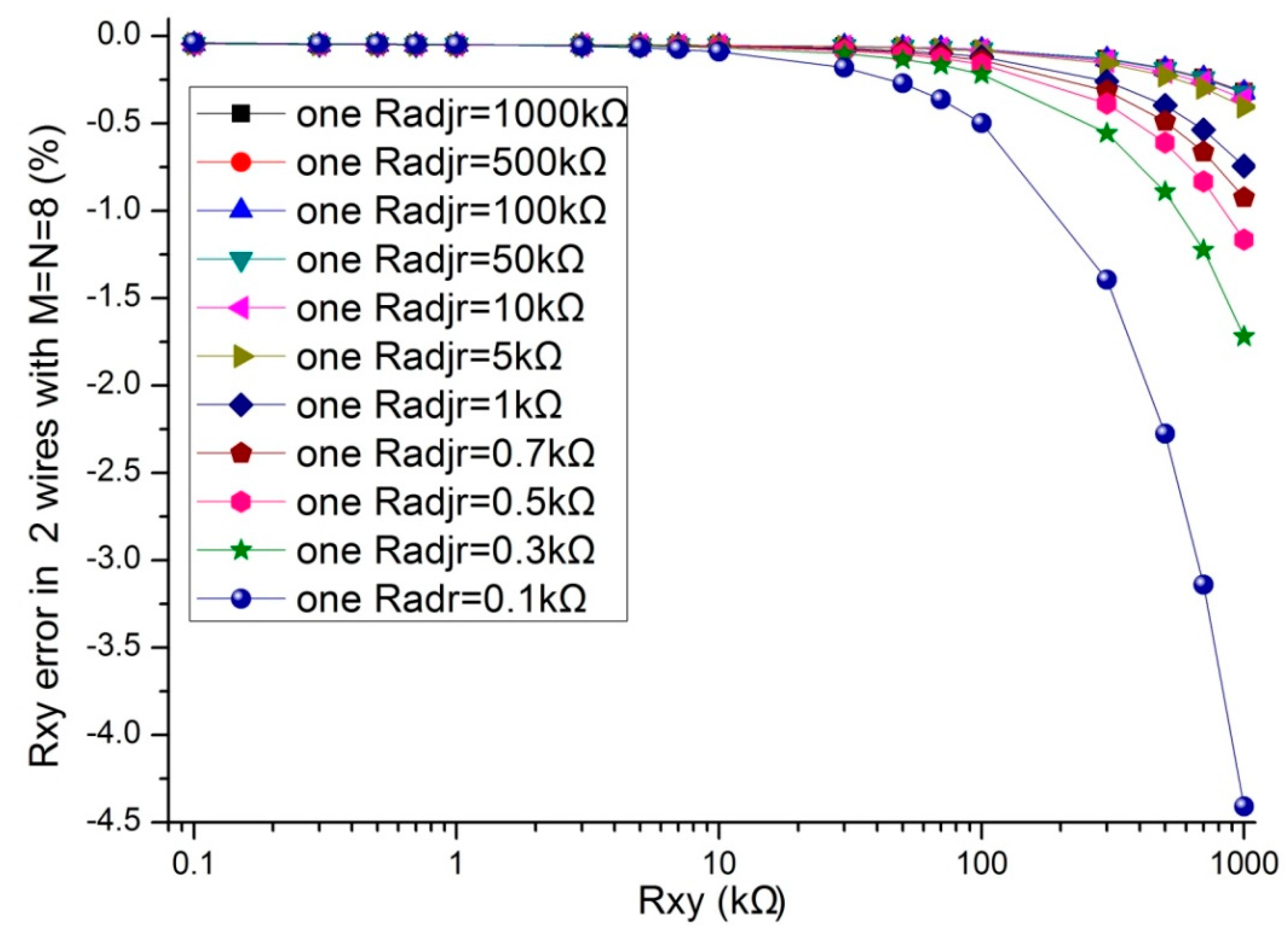
From the above discussion, the two-wire voltage feedback method can suppress the crosstalk caused by the row wires and the column wires, such as Rsrs, RLrs, Rscs, and RLcs.


