Article

Tunable Multiple-Step Plasmonic Bragg Reflectors with Graphene-Based Modulated Grating

1
School of Science, Jiangsu Provincial Research Center of Light Industrial Optoelectronic Engineering and Technology, Jiangnan University, Wuxi 214122, China
2
Key Laboratory of Semiconductor Materials Science, Institute of Semiconductors, Chinese Academy of Sciences, P.O. Box 912, Beijing 100083, China
*
Author to whom correspondence should be addressed.
Sensors 2016, 16(12), 2039; https://doi.org/10.3390/s16122039
Submission received: 17 October 2016 / Revised: 25 November 2016 / Accepted: 25 November 2016 / Published: 1 December 2016
(This article belongs to the Section Physical Sensors)

Abstract

:
We propose a novel plasmonic Bragg reflector (PBR) based on graphene with multiple-step silicon structure. The monolayer graphene bears locally variable optical properties by modulation of electric fields, and the periodical change of effective refractive index on graphene can be obtained by external bias voltage in the mid-infrared region. Through patterning the PBR units into multiple-step structures, we can decrease the insertion loss and suppress the rippling in transmission spectra. By introducing the defect into the multiple-step PBRs, the multiple resonance modes are formed inside the stopband by increasing the step number. This work may pave the ways for the further development of ultra-compact low-cost hyperspectral sensors in the mid-infrared region.

1. Introduction

Recently, graphene has become a popular research field and has attracted an increasing amount of attention [1]. Graphene, as a monolayer of carbon atoms arranged in a honeycomb lattice, offers a promising platform to overcome these obstacles [2,3]. Due to the unique electronic structure and dynamic tunability, graphene bears stronger mode confinement and lower propagation losses, and can be tuned by applying external gate voltages [4,5]. Graphene plasmonics, similar to metal plasmonics at the visible region, can be easily induced in the near-infrared to terahertz (THz) regime. In particular, the surface charge density, namely the chemical potential, can be actively modified via chemical doping or with the external gate voltage, thus giving rise to dramatic changes in the optical properties [6]. Surface plasmon polaritons (SPPs) bound to graphene display a strong field confinement, already verified by experiments [7,8]. These remarkable and outstanding properties enable a utility optical material in optoelectronic applications. Consequently, more attention has been focused on graphene-based plasmonic waveguides [9,10,11,12,13,14,15,16,17] in recent years. In addition, the tunable nano-modulators based on graphene plasmonic waveguide modulators have been proposed and numerically demonstrated [18]. Lu et al. have designed a slow-light waveguide based on graphene and silicon graded grating [19]. The tunable plasmonic Bragg reflectors based on graphene silicon waveguide have been presented and studied [20].
In this paper, the plasmonic Bragg reflector (PBR) structure based on graphene with multiple-step units are numerically presented in the mid-infrared region. External bias voltages are applied to control the optical properties of the graphene, and the periodical modulation of effective refractive index on graphene is obtained to form a forbidden band on transmitted spectrum. The insertion loss is lower and the rippling in transmission is suppressed by increasing the step number of multiple-step structures. Furthermore, multiple peaks appear in the stopband while the defect introduces into the multiple-step PBRs. The finite element method (FEM) has been utilized to perform simulation work.

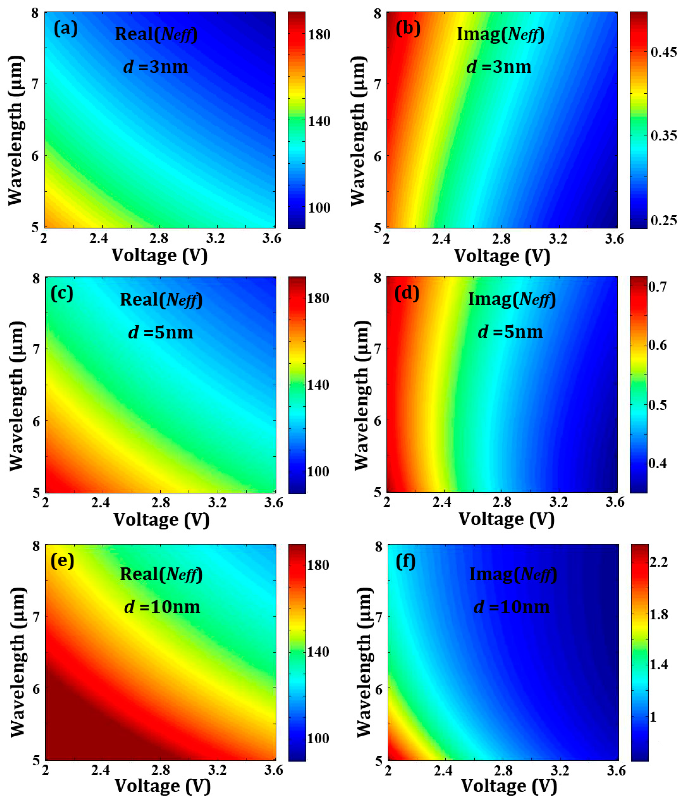
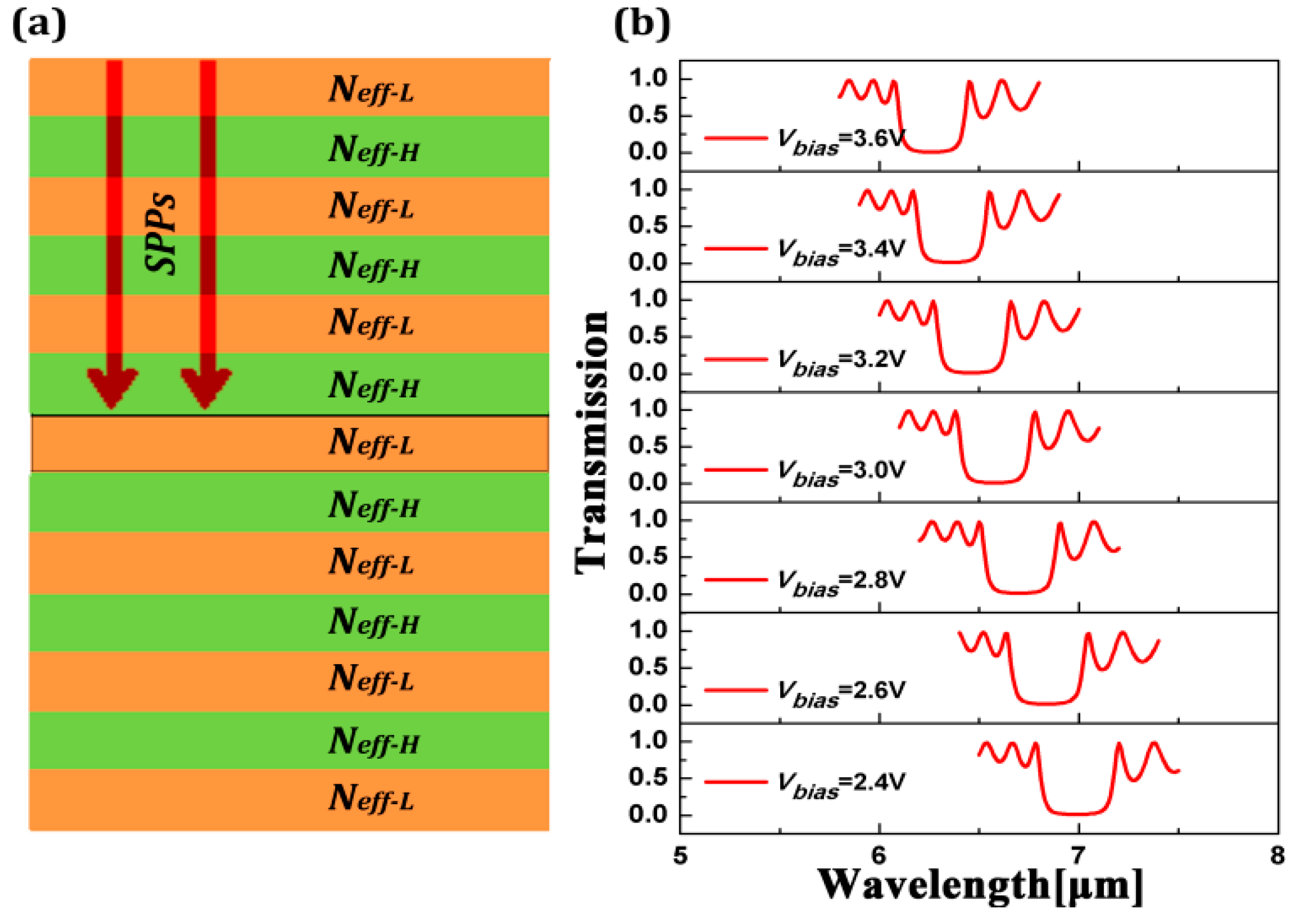
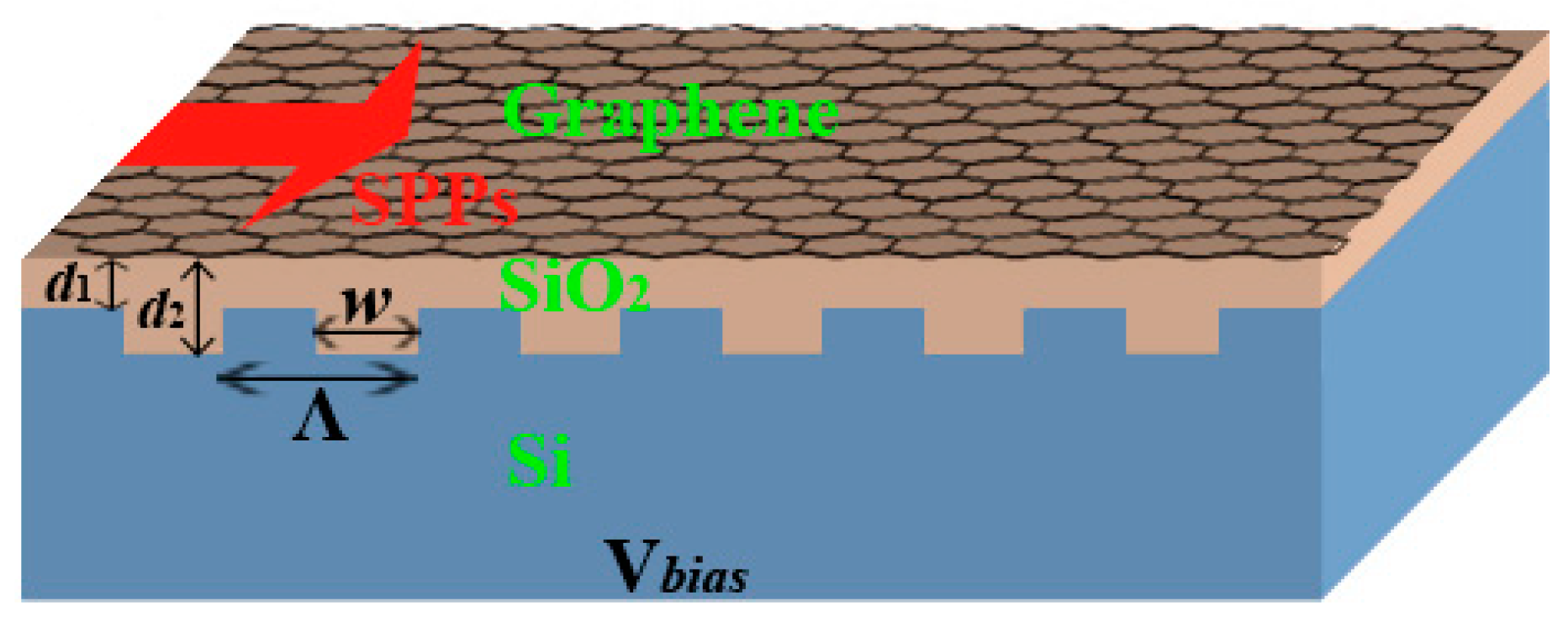
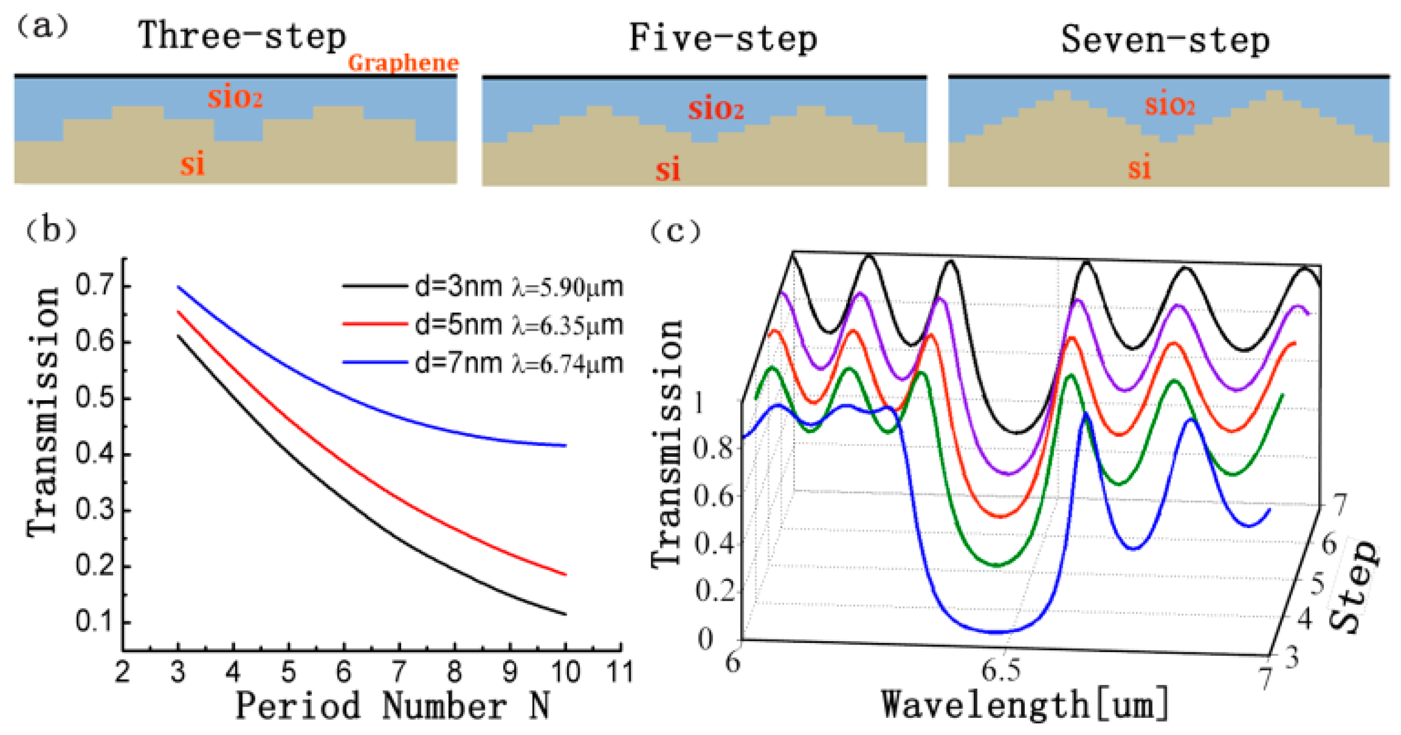
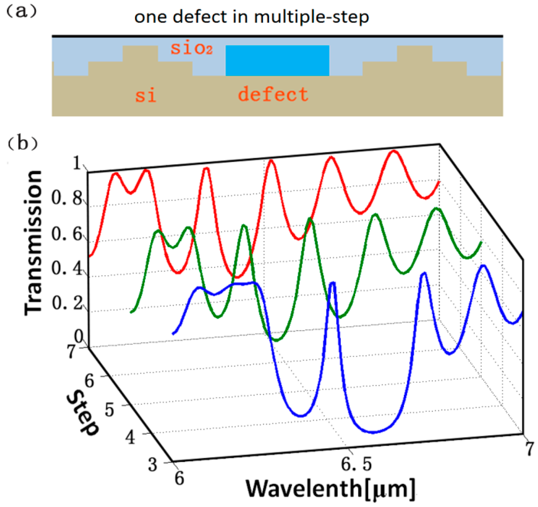
2. Model and Theoretical Analysis

The schematic of the PBR structure we proposed is shown in Figure 1. It consists of a monolayer graphene and a finite array of periodic highly doped silicon-based grating, and they are separated by a thin layer of silica. When a biased voltage Vbias is applied between graphene and silicon grating, the periodic induced electric field can be obtained and modulated in graphene due to the periodic grating structure. This theoretic structure is not hard to build up experimentally. The grating silica/silicon substrate can be fabricated via electron beam lithography. The monolayer graphene can be prepared by the chemical vapor deposition method and then placed on the grating substrate. When a broadband mid-infrared irradiation is incident on the structure from the left interface, SPPs will be excited and propagate along the graphene layer. According the Bragg condition, only a narrowband of the spectrum can pass through the graphene waveguide and the rest will be reflected away., We set d(y), i.e., d1 and d2 labeled in Figure 1, as the thickness of the SiO2 thin layer, which is a periodic step function of y, and it is far less than the width of the trench in the grating. We assume the field is given by the equation E(y) = εSiO2V/d(y); here, V = Vbias, and εSiO2 is the relative permittivity of SiO2. Then, the surface charge density of graphene can be approximated by n(y) = [ε0E(y)]/e = ε0εSiO2V/ed(y); here, ε0 is the vacuum permittivity, and e is the elementary charge. Further, we can modulate the Fermi level according to Ef(y) = ħνf(πns)1/2; here, νf = 106 m/s is the Fermi velocity of the electron in the graphene, and ħ is the reduced Planck constant. The Fermi level affects the scattering of electrons, characterized by the relaxation time τ = μEf(y)/f2; here, μ is the carrier mobility. According to Kubo formula, the optical properties of a monolayer graphene can be characterized by a complex surface conductivity σG [11]:
σ G ( y ) = 2 i e 2 k B T π 2 [ ω + i τ ( y ) 1 ] l n [ 2 c o s h [ E f ( y ) 2 k B T ] ] + i e 2 4 π l n [ 2 E f ( y ) [ ω + i τ ( y ) 1 ] 2 E f ( y ) + [ ω + i τ ( y ) 1 ] ]
The first term and the second term correspond to intraband transitions and interband transitions, respectively, where kB is the Boltzmann constant, T is the temperature, and w is the angular frequency of optical excitation.
In our work, the permittivity of graphene layer [21,22,23] can be characterized by a dielectric function:
ε G = ε b + i σ G ε 0 ω t G
where εb and tG are typically chosen as 2.5 and 1 nm, respectively. The optical parameters of other involved materials are εAir = 1, εSiO2 = 3.9, and εSi = 11.7 in the spectral region of interest. In our study, the values of voltages and the parameters of the structure are dependent on each other and should be reasonably chosen.
We regard the structure as an Air-Graphene-SiO2-Si multi-layer structure. According to Maxwell’s equations and the boundary conditions, the general dispersion relation for the graphene waveguide in the multilayer structures can be solved by the following equation:
ε 1 N e f f 2 ε 1 + ε 2 N e f f 2 ε 2 = i σ G η 0
where η0 is the intrinsic impedance of free space. If ε1 = ε2 = ε, the effective refractive can be reduced from Equation (3) as follows:
N e f f = Re ( 1 ( 2 σ G η 0 ) 2 )
The relation of the effective refractive Neff (both real and imaginary parts) with bias voltage V and wavelength λ is well depicted in Figure 2a–d. Here, the carrier mobility is μ = 2 m2·V−1·s−1, and the real parts are invariant while the imaginary parts decrease dramatically as μ increases.

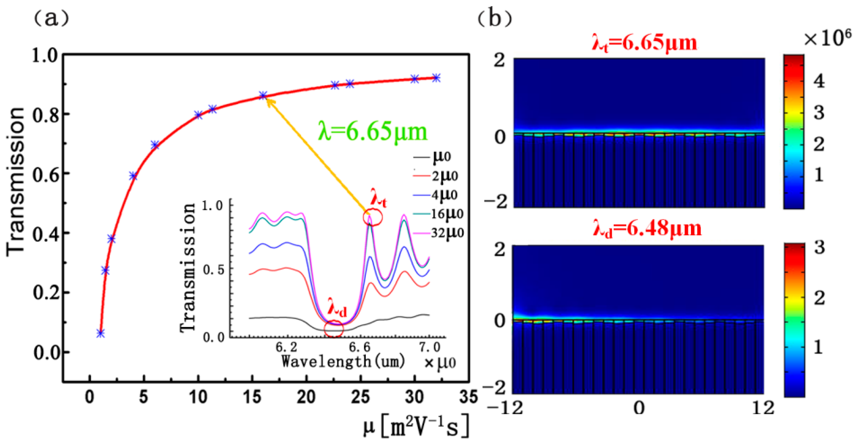
3. Simulations and Results

The loss of the graphene-based structure is mainly caused by the imaginary part of complex permittivity of graphene. Here, we firstly consider the real part of complex permittivity of graphene and its lossless style. When SPPs propagate in periodically modulating media, we can regard the graphene-based silica grating structure as a Bragg reflector made of alternating layers with a high reflective index (Neff-H) and a low reflective index (Neff-L), as shown in Figure 3a. The partial reflection will happen in each boundary due to the mismatch between the adjacent effective refractive index. High reflection will occur if the reflected beams superpose constructively and a stop-band will appear in the transmission spectrum, as shown in Figure 3b. We can see that the position of the stop-band is blue-shifted as Vbias increases. Here, the parameters are set as d1 = 5 nm, d2 = 10 nm, w = 40 nm, and Ʌ = 80 nm.
Furthermore, we design the PBR units into the multi-step pattern to deal with the high insertion loss and severe rippling in the transmission spectra resulting from the abrupt change of Neff in the groove depth [24,25]. The 2D schematic of the three-step, five-step, and seven-step versions of the PBR units are illustrated in Figure 4a. For the three-step PBR unit, we plot the transmission spectra in Figure 4b versus the period number N changing with deferent SiO2 thickness d and wavelength λ. After comparing the transmission spectra in Figure 4c, we find the expected enhancement on transmission spectra and rippling suppression. Additionally, the stopband is gradually narrowed when the PBR unit is changed into more steps. The multiple steps in a PBR unit actually adding multiple reflections in the Bragg reflections process make it harder to satisfy the Bragg conditions, which results in sidelobe suppression and a narrowed stopband.
In order to make the practical application of this ideal platform more extensive, we designed one defect structure in the multiple-step PBR reflectors to realize the filtering, as shown in Figure 5a. The parameters of the structures and the gate voltage are the same as those in Figure 4a, where the width of the defect t = 100 nm, and the gate voltage Vg = 2.2 V. From Figure 5b, we can see that one peak appears in the stopband of the transmission spectrum for the three-step structure with the defect and two peaks for the five-defect and seven-defect structures, and that their resonance wavelengths of the projection have a slight red-shift and the transmissions of the peak are almost invariant when increasing the step number. The relative wide bandgaps near those peaks always exist. Those sharp projections, obtained by the hybrid effects of the first order mode resonance and high order mode resonance, can be regularly adjusted in a reasonable wavelength range.
Finally, we need to consider the material losses of graphene. As shown in Figure 6a, using the three-step structure as an example, the value of the transmission peak will increase with the increasing of carrier mobilities. In other words, the carrier mobility exerts an effect on the imaginary part of the effective refractive Neff of graphene. This corresponds to the preceding statement. Another conspicuous feature is that the effect decreases with the increase in carrier mobility when it exceeds 20 m2·V−1·s−1. Thus, we can consider the losses negligible in this case, and it can be realized by using proper doping or compensating the gain media. In Figure 6b, we plot the distributions of the electric field at excitation wavelengths λt and λr in the case of Vbias = 3.2 V in order to visualize the propagating principle of the excited SPPs.

4. Conclusions

We have here presented some plasmonic Bragg reflectors based on graphene to realize the tunable low-loss filtering effect in the broadband multiple-step structures, and PBRs feasibilities have been adequately verified by FEM. By modulating the bias voltages of graphene, we can turn the transmission spectrum according to our need. Moreover, the transmission can reach above 80%, which means the losses are quite low as long as the carrier mobility is large enough. In addition, by designing the PRB units into multi-step structures, we can mitigate the insertion loss and suppress the rippling in transmission spectra. We introduced the defect structure in the multiple-step PBR reflectors to realize multiple filtering phenomena. These proposed designs were easily carried out in experiment. We hope they can help pave new ways in actively tunable sensoring applications.

Acknowledgments

This work is supported by the National Natural Science Foundation of China (Grant No. 11504139), the Natural Science Foundation of Jiangsu Province (Grant No. BK20140167), the Fundamental Research Funds for the Central Universities (Grant No. JUSRP51517), and the Key Laboratory Open Fund of Institute of Semiconductors of CAS (Grant No. KLSMS-1405).

Author Contributions

J.W. and H.S. conceived the idea. Q.Q., Y.L., M.Z. and Y.L. calculated properties of the proposed structure, analyzed the data, and wrote the manuscript. J.W., H.Y. and Y.L. revised the manuscript. J.W. supervised the project. All authors read and approved the final manuscript.

Conflicts of Interest

The authors declare no conflict of interest.

References

  1. Li, Z.Q.; Henriksen, E.A.; Jiang, Z.; Hao, Z.; Martin, M.C.; Kim, P.; Stormer, H.L.; Basov, D.N. Dirac charge dynamics in graphene by infrared spectroscopy. Nat. Phys. 2008, 4, 532–535. [Google Scholar] [CrossRef]
  2. Novoselov, K.S.; Geim, A.K.; Morozov, S.V.; Jiang, D.; Zhang, Y.; Dubonos, S.V.; Grigorieva, I.V.; Firsov, A.A. Electric Field Effect in Atomically Thin Carbon Films. Science 2004, 306, 666–669. [Google Scholar] [CrossRef] [PubMed]
  3. Geim, A.K.; Novoselov, K.S. The rise of graphene. Nat. Mater. 2007, 6, 183–191. [Google Scholar] [CrossRef] [PubMed]
  4. Polman, A.; Atwater, H.A. Photonic design principles for ultrahigh-efficiency photovoltaics. Nat. Mater. 2012, 11, 174–177. [Google Scholar] [CrossRef] [PubMed]
  5. Liu, M.; Zhang, X. Silicon photonics: Graphene benefits. Nat. Photonics 2013, 7, 851–852. [Google Scholar] [CrossRef]
  6. Wang, F.; Zhang, Y.; Tian, C.; Girit, C.; Zettl, A.; Crommie, M.; Shen, Y.R. Gate-variable optical transitions in graphene. Science 2008, 320, 206–209. [Google Scholar] [CrossRef] [PubMed]
  7. Fei, Z.; Rodin, A.S.; Andreev, G.O.; Bao, W.; McLeod, A.S.; Wagner, M.; Zhang, L.M.; Zhao, Z.; Thiemens, M.; Dominguez, G.; et al. Gate-tuning of graphene plasmons revealed by infrared nano-imaging. Nature 2012, 487, 82–85. [Google Scholar] [CrossRef] [PubMed]
  8. Brar, V.W.; Jang, M.S.; Sherrott, M.; Lopez, J.J.; Atwater, H.A. Highly confined tunable mid-infrared plasmonics in graphene nanoresonators. Nano Lett. 2013, 13, 2541–2547. [Google Scholar] [CrossRef] [PubMed]
  9. Lu, H.; Cumming, B.P.; Gu, M. Highly efficient plasmonic enhancement of graphene absorption at telecommunication wavelengths. Opt. Lett. 2015, 40, 3647–3650. [Google Scholar] [CrossRef] [PubMed]
  10. Wang, X.; Xia, X.; Wang, J.; Zhang, F.; Hu, Z.D.; Liu, C. Tunable plasmonically induced transparency with unsymmetrical graphene-ring resonators. J. Appl. Phys. 2015, 118, 013101. [Google Scholar] [CrossRef]
  11. Wang, B.; Zhang, X.; Vidal, F.J.G.; Yuan, X.C.; Teng, J.H. Strong coupling of surface plasmon polaritons in monolayer graphene sheet arrays. Phys. Rev. Lett. 2012, 109, 073901. [Google Scholar] [CrossRef] [PubMed]
  12. Liu, P.Q.; Luxmoore, I.J.; Mikhailov, S.A.; Savostianova, N.A.; Valmorra, F.; Faist, J.; Nash, G.R. Highly tunable hybrid metamaterials employing split-ring resonators strongly coupled to graphene surface plasmons. Nat. Commun. 2015, 6, 8969. [Google Scholar] [CrossRef] [PubMed] [Green Version]
  13. Atre, A.C.; Brenny, B.J.; Coenen, T.; Polman, A.; Dionne, J.A. Nanoscale optical tomography with cathodoluminescence spectroscopy. Nat. Nanotechn. 2015, 10, 429–436. [Google Scholar] [CrossRef] [PubMed]
  14. Deng, H.; Yan, Y.; Xu, Y. Tunable flat-top bandpass filter based on coupled resonators on a graphene sheet. IEEE Photon. Techn. Lett. 2015, 27, 1161–1164. [Google Scholar] [CrossRef]
  15. Wang, X.; Chen, C.; Pan, L.; Wang, J. A graphene-based Fabry-Pérot spectrometer in mid-infrared region. Sci. Rep. 2016, 6, 32616. [Google Scholar] [CrossRef] [PubMed]
  16. Chen, Y.; Song, Z.; Li, Y.; Hu, M.; Xing, Q.; Zhang, Z.; Chai, L.; Wang, C.Y. Effective surface plasmon polaritons on the metal wire with arrays of subwavelength grooves. Opt. Express 2006, 14, 13021–13029. [Google Scholar] [CrossRef] [PubMed]
  17. Chen, Y.; Zhang, Z.; Yu, M. Tunable out-of-plane slow light in resonance induced transparent grating waveguide structures. Appl. Phys. Lett. 2013, 103, 061109. [Google Scholar] [CrossRef]
  18. Lao, J.; Tao, J.; Wang, Q.; Huang, X. Tunable graphene-based plasmonic waveguides: Nano modulators and nano attenuators. Laser Photonics Rev. 2014, 8, 569–574. [Google Scholar] [CrossRef]
  19. Lu, H.; Zeng, C.; Zhang, Q.; Liu, X.; Hossain, M.M.; Reineck, P.; Gu, M. Graphene-based active slow surface plasmon polaritons. Sci. Rep. 2015, 5, 8443. [Google Scholar] [CrossRef] [PubMed]
  20. Tao, J.; Yu, X.; Hu, B.; Dubrovkin, A.; Wang, Q.J. Graphene-based tunable plasmonic Bragg reflector with a broad bandwidth. Opt. Lett. 2014, 39, 271–274. [Google Scholar] [CrossRef] [PubMed]
  21. Nesterov, M.L.; Abad, J.B.; Nikitin, A.Y.; Vidal, F.J.G.; Moreno, L.M. Graphene supports the propagation of subwavelength optical solitons. Laser Photon. Rev. 2013, 7, L7–L11. [Google Scholar] [CrossRef]
  22. Vakil, A.; Engheta, N. Transformation optics using graphene. Science 2011, 332, 1291–1294. [Google Scholar] [CrossRef] [PubMed]
  23. Gao, W.; Shu, J.; Qiu, C.; Xu, Q. Excitation of Plasmonic Waves in Graphene by Guided-Mode Resonances. ACS Nano 2012, 6, 7806–7813. [Google Scholar] [CrossRef] [PubMed]
  24. He, X.Y.; Li, R. Comparison of Graphene-Based Transverse Magnetic and Electric Surface Plasmon Modes. IEEE J. Sel. Top. Quantum Electron. 2014, 20, 4600106. [Google Scholar]
  25. Qu, S.; Song, C.; Xia, X.; Liang, X.; Tang, B.; Hu, Z.D.; Wang, J. Detuned plasmonic Bragg grating sensor based on defect metal-insulator-metal waveguide. Sensors 2016, 16, 784. [Google Scholar] [CrossRef] [PubMed]
Figure 1. Schematic of the structure of a plasmonic Bragg reflector and the structure parameters are w = 40 nm and Ʌ = 80 nm. Voltage Vbias is applied between graphene and silicon grating.
Sensors 16 02039 g001
Figure 2. (a,c,e) The real part and (b,d,f) the imaginary part of the effective reflective index of graphene Neff as a function of applied voltage V and wavelength λ for d = 3 nm, d = 5 nm, and d = 10 nm. Here, the carrier mobility is μ = 2 m2·V−1·s−1.
Sensors 16 02039 g002
Figure 3. (a) The principle model of the graphene waveguide, and Neff-L and Neff-H are the effective reflective index of graphene at sections of d1 = 5 nm and d2 = 10 nm, respectively; (b) The position of the stop-band in the transmission spectrum can be controlled by changing the bias voltage Vbias.
Sensors 16 02039 g003
Figure 4. (a) The 2D schematic illustration of the PBR unit designed into multiple-step patterns: three-step PBR unit, five-step PRB unit, and seven-step PBR unit, respectively; (b) The transmission of the three-step PBR with a different period number N; (c) The transmission of the PBRs for different cases from the three-step to seven-step pattern structures, respectively. Here, d is set as 5 nm, w = 20 nm, the period number N = 6, and the bias voltages Vbias = 3.2 V.
Sensors 16 02039 g004
Figure 5. (a) Schematic illustration of 2D profiles of multiple-step structure with one defect; (b) The transmission of PBRs with the defect for different cases from the three-step to seven-step pattern structures, respectively. The parameters of the structures and the bias voltages are the same as those in Figure 4a. Here, the width of the defect t = 100 nm, and the gate voltage Vg = 2.2 V.
Sensors 16 02039 g005
Figure 6. (a) The transmission at λt = 6.65 μm as a function of carrier mobility for the three-step structure considering the material losses of graphene. The inset is the transmission spectrum for a different carrier mobility μ. Here, μ0 is set as 1 m2·V−1·s−1, and the bias voltages are Vbias = 3.2 V; (b) The 2D distributions of the electric field |E|2 at excitation wavelengths λt and λr when Vbias = 3.2 V.
Sensors 16 02039 g006

