
A Low-Power All-Digital on-Chip CMOS Oscillator for a Wireless Sensor Node

Abstract
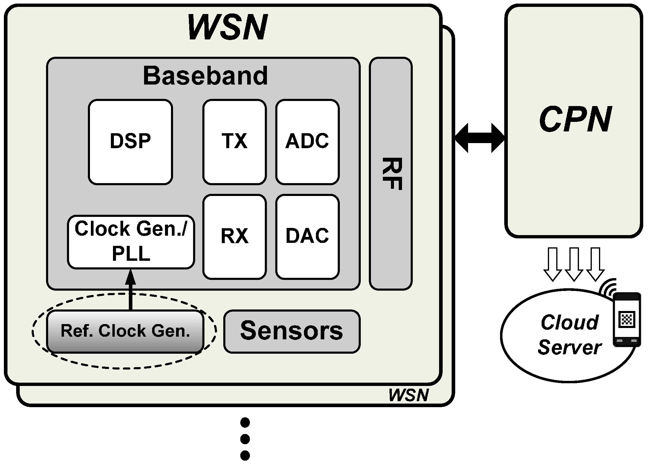
:1. Introduction
2. Review of Conventional DCOs
3. Proposed DCO Design
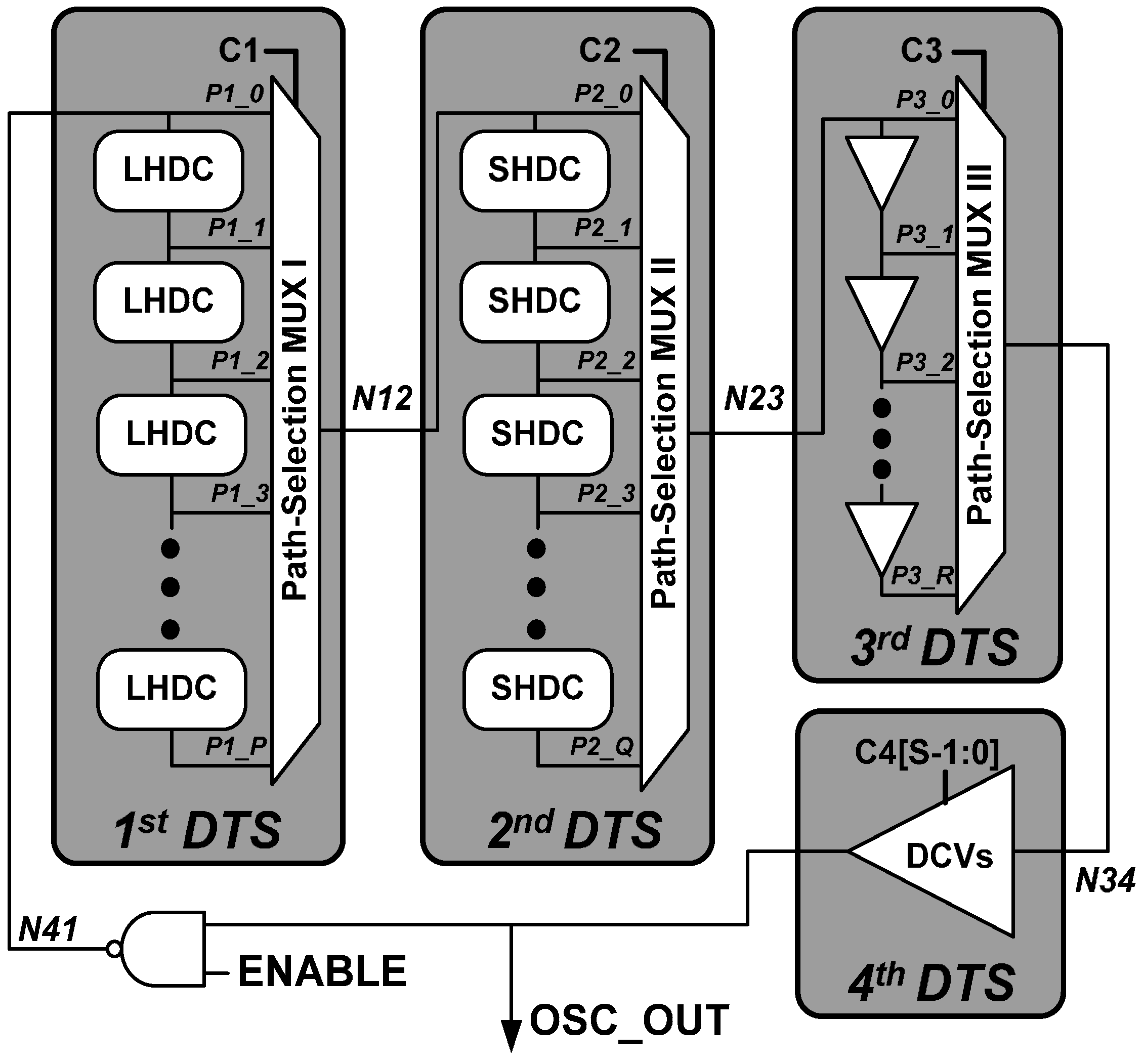
3.1. Architecture
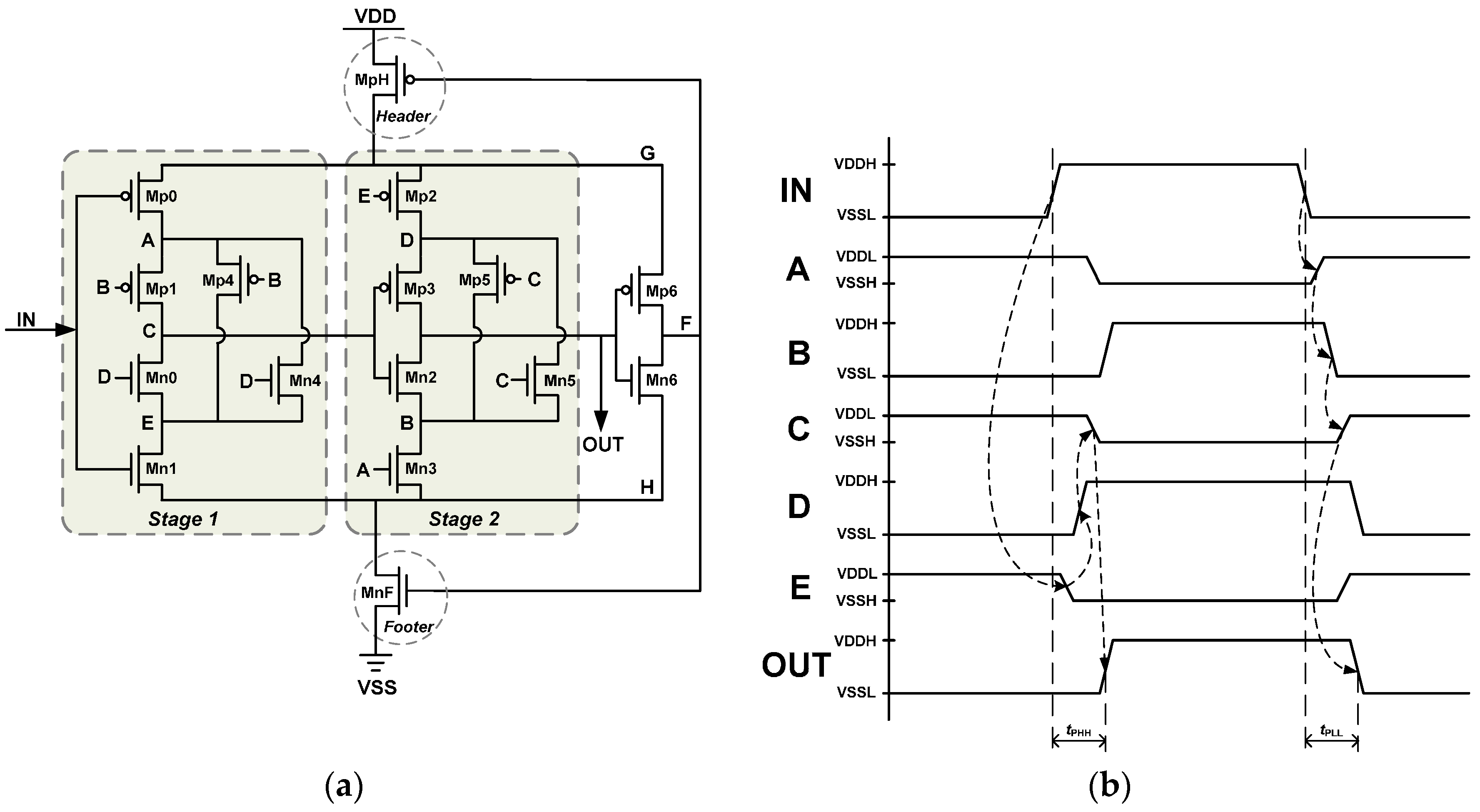
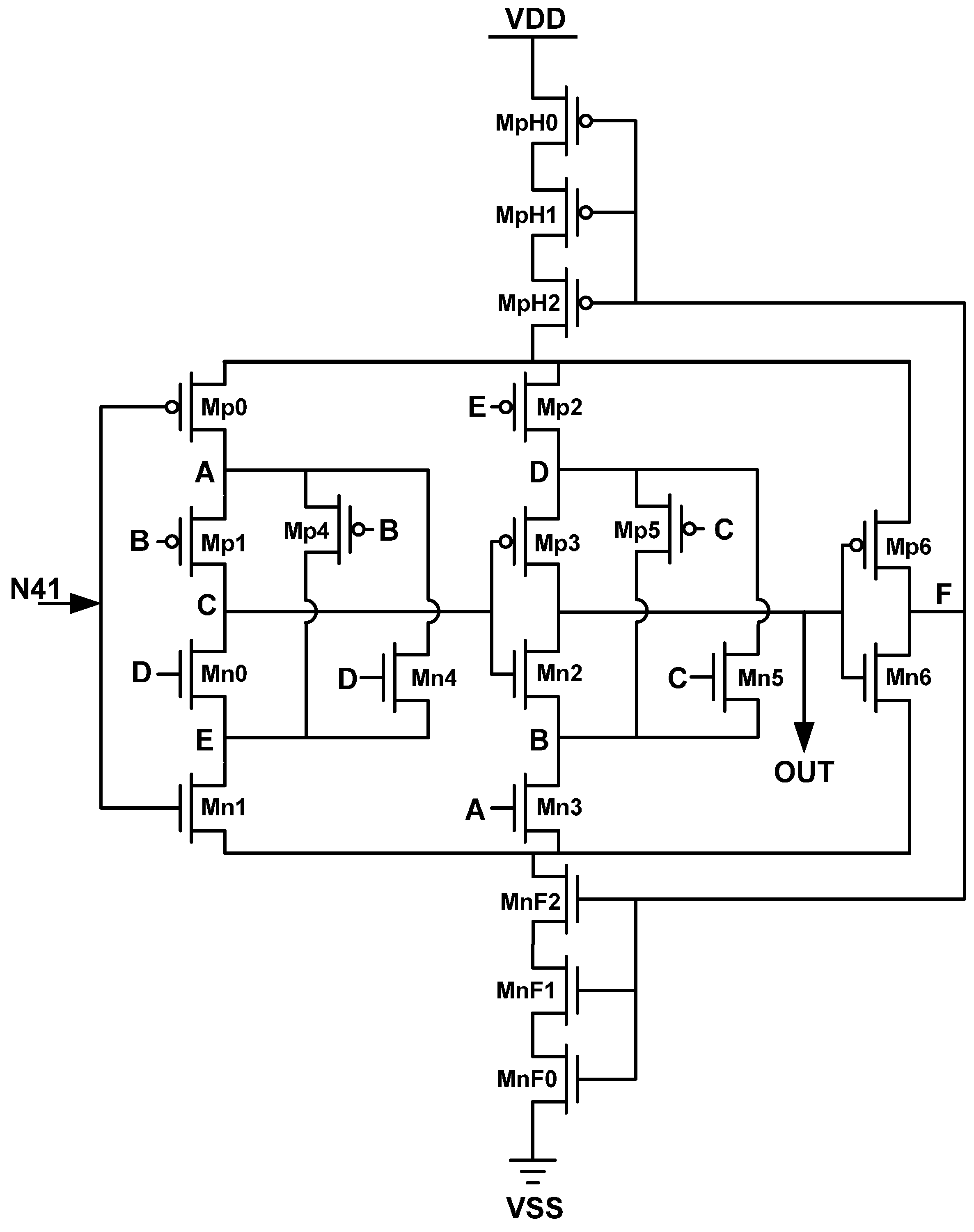
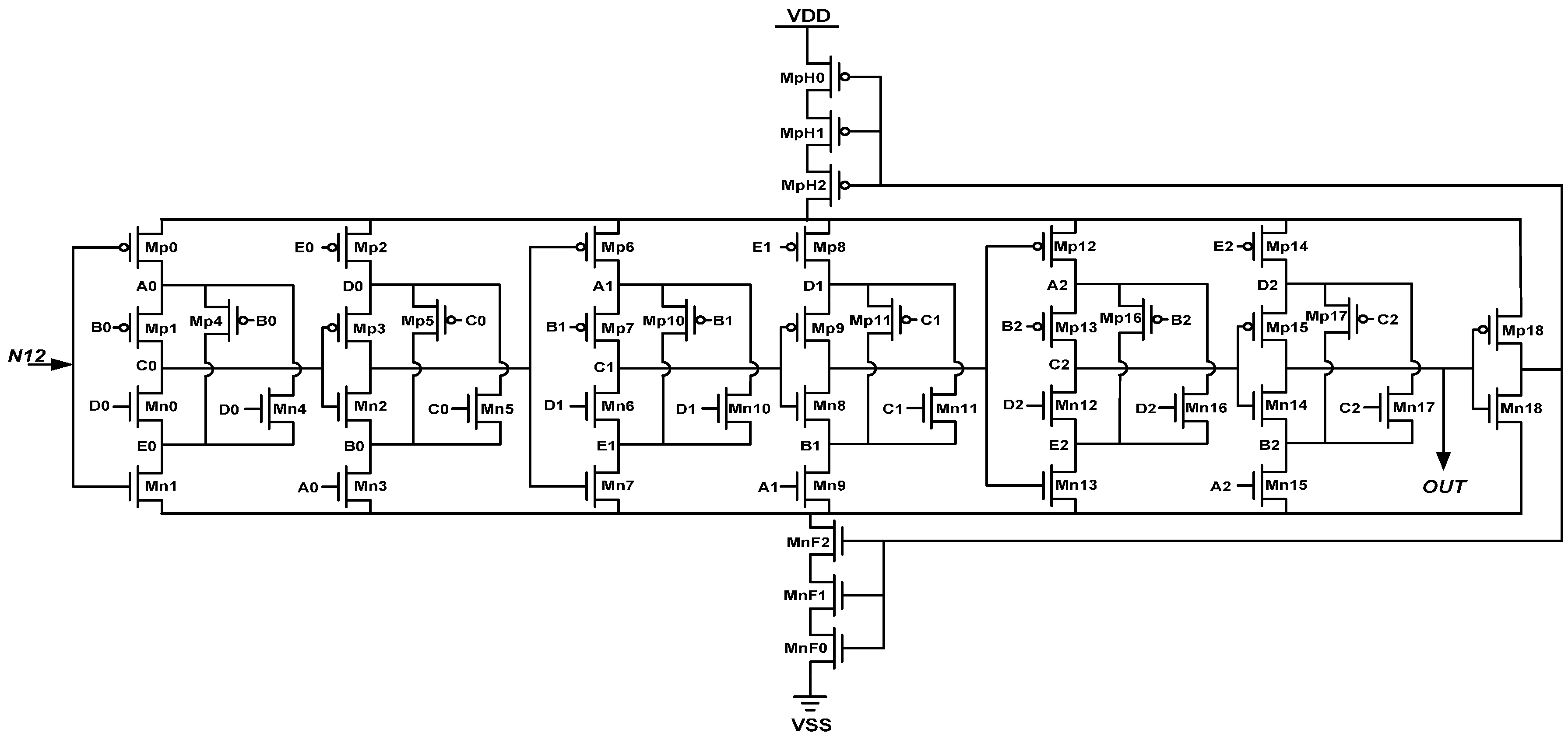
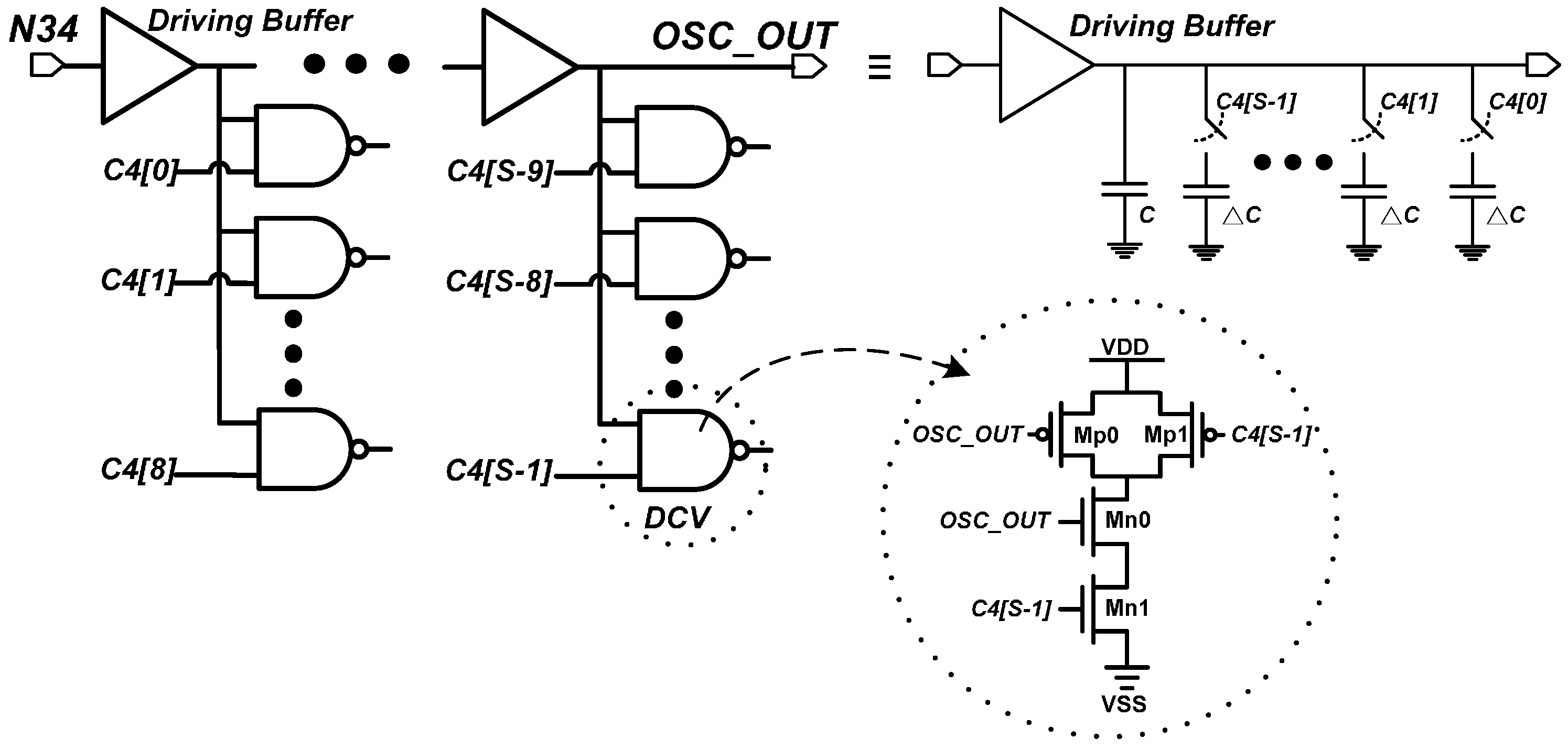
3.2. Circuit Implementation
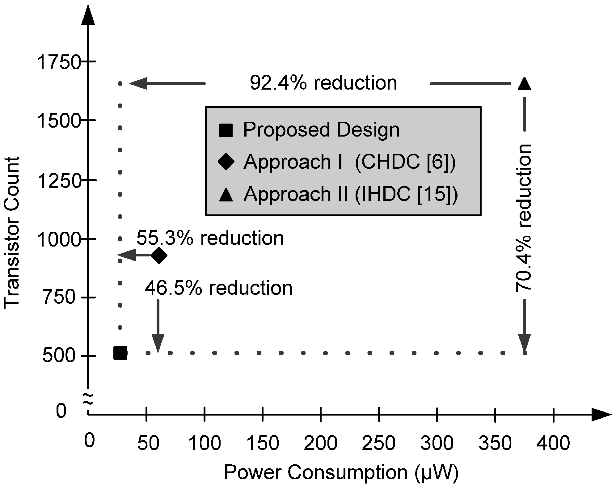
4. Delay Cell Comparisons
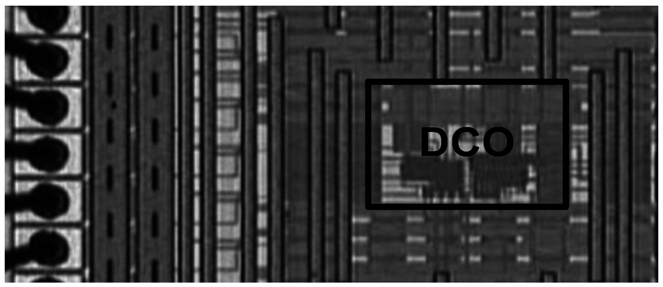
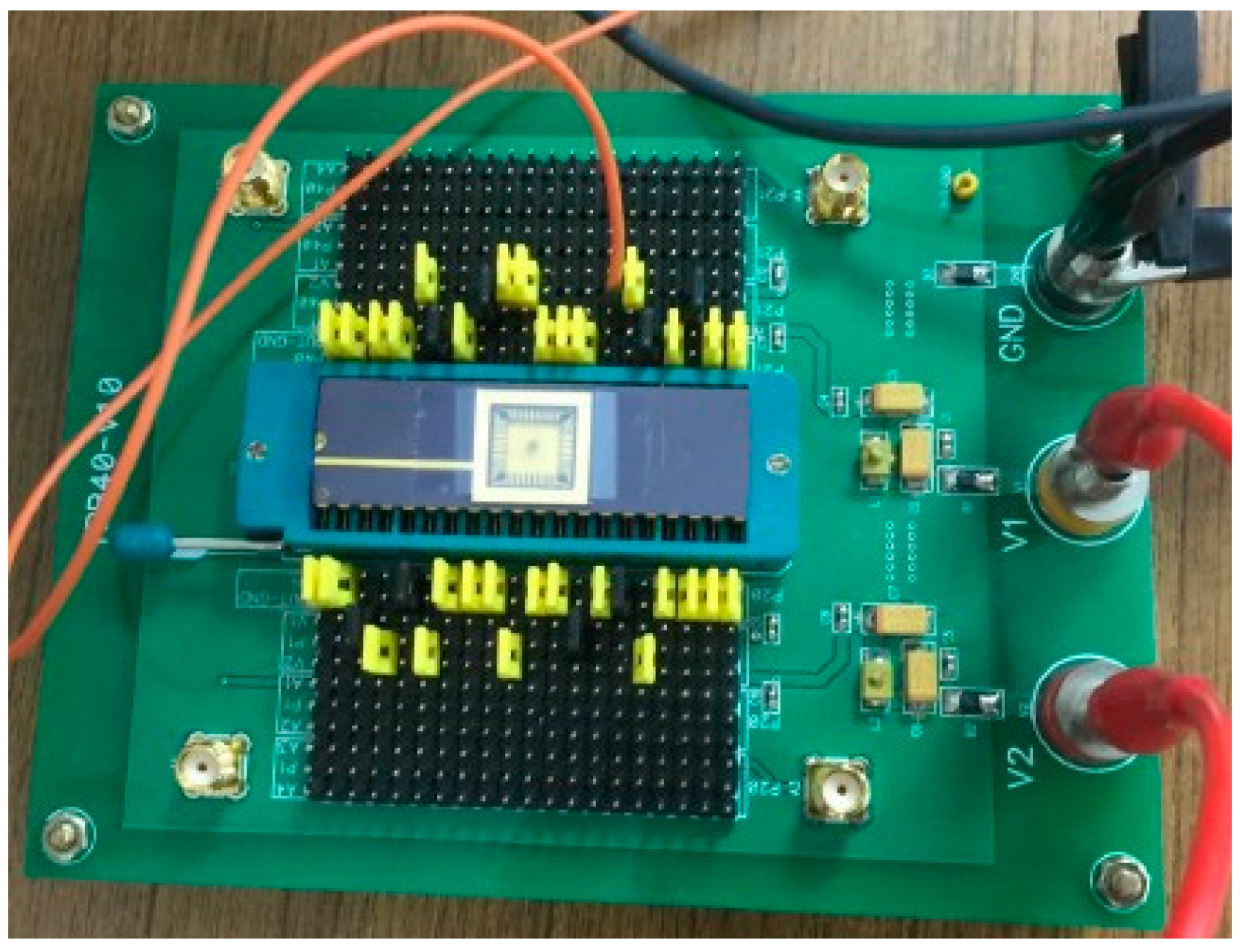
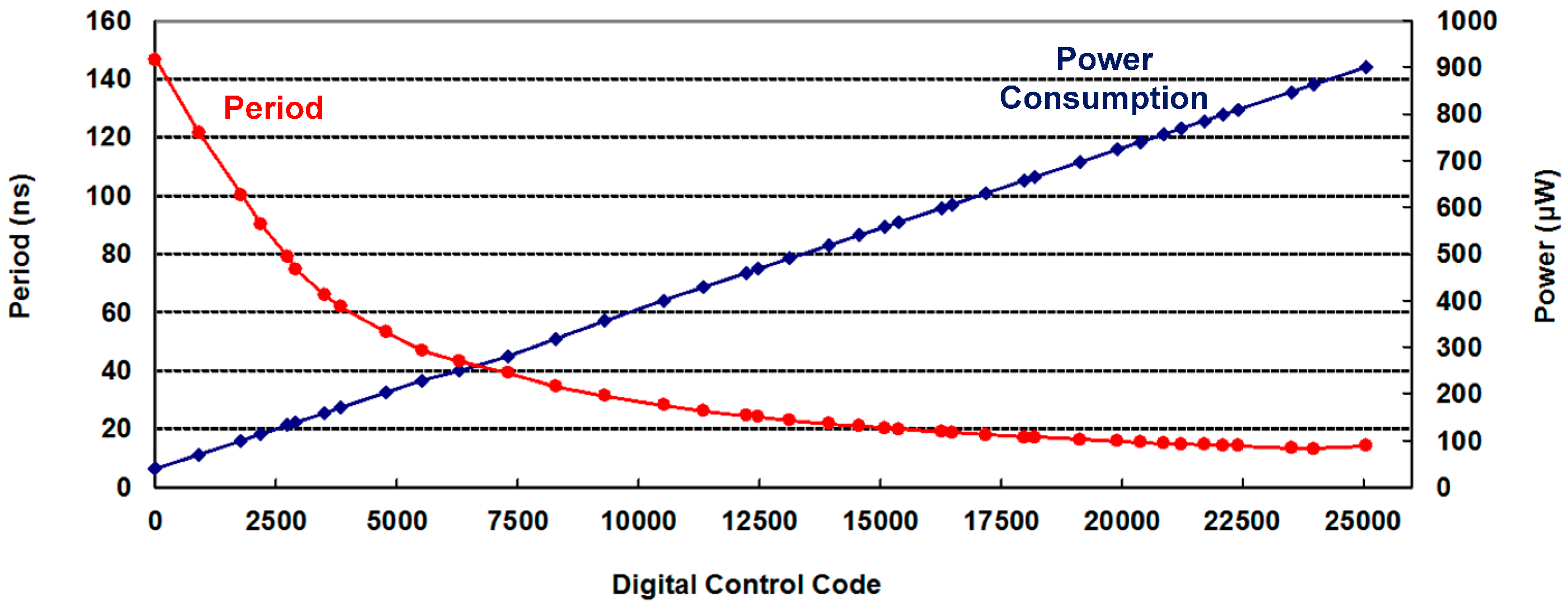
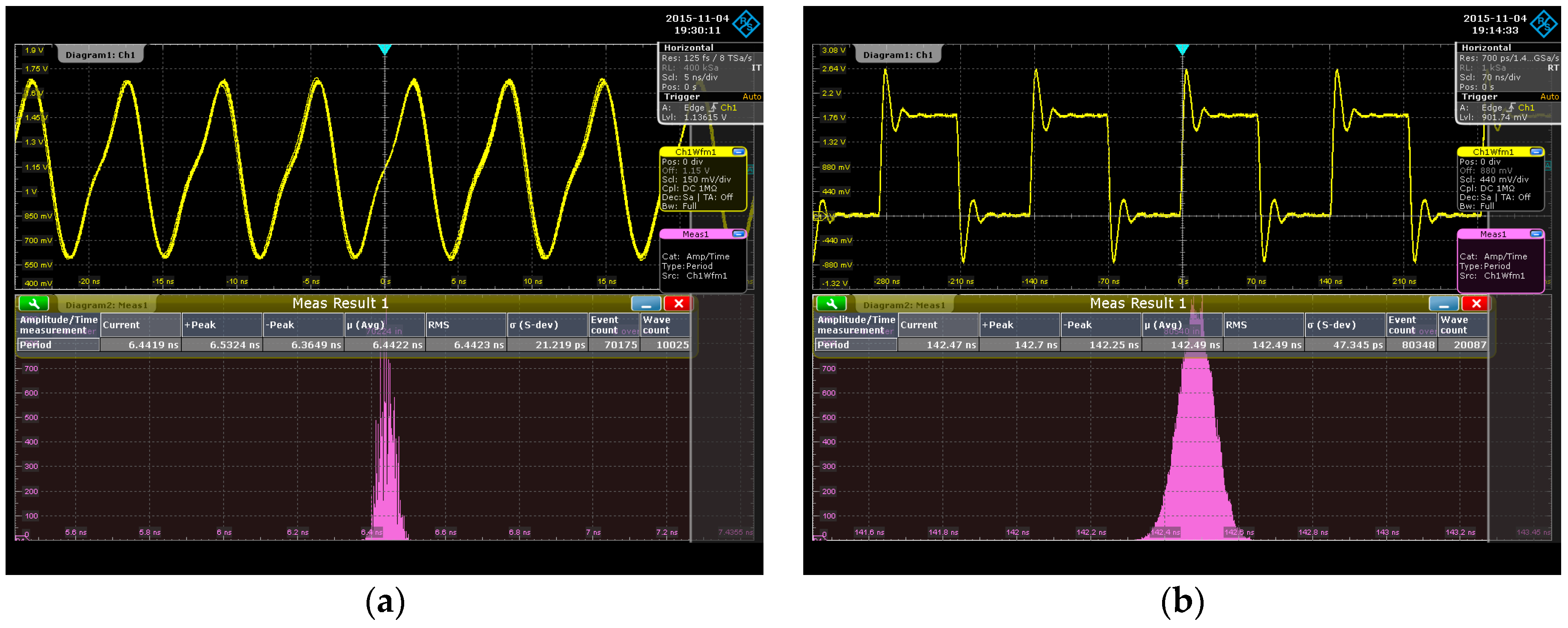
5. Experimental Results and Discussions
6. Conclusions
Acknowledgments
Author Contributions
Conflicts of Interest
References
- Otto, C.A.; Jovanov, E.; Milenkovic, A.A. WBAN-based system for health monitoring at home. In Proceedings of the 3rd IEEE-EMBS International Summer School and Symposium on Medical Devices and Biosensors, Boston, MA, USA, 4–6 September 2006; pp. 20–23.
- Chen, T.-W.; Yu, J.-Y.; Yu, C.-Y.; Lee, C.-Y. A 0.5 V 4.85 Mbps dual-mode baseband transceiver with extended frequency calibration for biotelemetry applications. IEEE J. Solid-State Circuits 2009, 44, 2966–2976. [Google Scholar] [CrossRef] [Green Version]
- Body Area Networks (BAN), IEEE 802.15 WPAN Task Group 6, November 2007. Available online: http://www.ieee802.org/15/pub/TG6.html (accessed on 1 July 2014).
- Sung, W.-H.; Yu, J.-Y.; Lee, C.-Y.L. A robust frequency tracking loop for energy-efficient crystal-less WBAN systems. IEEE Trans. Circuits Syst. II Express Briefs 2011, 58, 637–641. [Google Scholar] [CrossRef]
- Lhermet, H.; Condemine, C.; Plissonnier, M.; Salot, R.; Audebert, P.; Rosset, M. Efficient power management circuit: Thermal energy harvesting to above-IC microbattery energy storage. In Proceedings of the IEEE International Solid-State Circuits Conference Digest of Technical Papers, San Francisco, CA, USA, 11–15 February 2007.
- Hsu, S.-Y.; Yu, J.-Y.; Lee, C.-Y. A sub-10-μW digitally controlled oscillator based on hysteresis delay cell topologies for WBAN applications. IEEE Trans. Circuits Syst. II Express Briefs 2010, 57, 951–955. [Google Scholar] [CrossRef]
- Choi, P.; Park, H.C.; Kim, S.; Park, S.; Nam, I.; Kim, T.W.; Park, S.; Shin, S.; Kim, M.S.; Kang, K.; et al. An experimental coin-sized radio for extremely low-power WPAN (IEEE 802.15.4) application at 2.4 GHz. IEEE J. Solid-State Circuits 2003, 38, 2258–2268. [Google Scholar] [CrossRef]
- Razavi, B. RF Microelectronics; Prentice-Hall: Englewood Cliffs, NJ, USA, 1998. [Google Scholar]
- Maymandi-Nejad, M.; Sachdev, M. A monotonic digitally controlled delay element. IEEE J. Solid-State Circuits 2005, 40, 2212–2219. [Google Scholar] [CrossRef]
- Staszewski, R.B.; Leipold, D.; Muhammad, K.; Balsara, P.T. Digitally controlled oscillator (DCO)-based architecture for RF frequency synthesis in a deep-submicrometer CMOS process. IEEE Trans. Circuits Syst. II Analog Digit. Signal. Process. 2003, 50, 815–828. [Google Scholar] [CrossRef]
- Olsson, T.; Nilsson, P. A digitally controlled PLL for SoC applications. IEEE J. Solid-State Circuits 2004, 39, 751–760. [Google Scholar] [CrossRef]
- Chung, C.-C.; Lee, C.-Y. An all digital phase-locked loop for high-speed clock generation. IEEE J. Solid-State Circuits 2003, 38, 347–351. [Google Scholar] [CrossRef]
- Chen, P.-L.; Chung, C.-C.; Lee, C.-Y. A portable digitally controlled oscillator using novel varactors. IEEE Trans. Circuits Syst. II Express Briefs 2005, 52, 233–237. [Google Scholar] [CrossRef]
- Sheng, D.; Chung, C.-C.; Lee, C.-Y. An ultra-low-power and portable digitally controlled oscillator for SoC applications. IEEE Trans. Circuits Syst. II Exp. Briefs 2007, 54, 954–958. [Google Scholar] [CrossRef]
- Yu, C.-Y.; Chung, C.-C.; Yu, C.-J.; Lee, C.-Y. A low-power DCO using interlaced hysteresis delay cells. IEEE Trans. Circuits Syst. II Exp. Briefs 2012, 59, 673–677. [Google Scholar] [CrossRef]
- Al-Sarawi, S.F. Low power Schmitt trigger circuits. Electron. Lett. 2002, 38, 1009–1010. [Google Scholar] [CrossRef]
- Chen, M.-C.; Yu, J.-Y.; Lee, C.-Y. A Sub-100 μW Area-Efficient Digitally-Controlled Oscillator Based on Hysteresis Delay Cell Topologies. In Proceedings of the IEEE Asian Solid-State Circuits Conference (ASSCC), Taipei, Taiwan, 16–18 November 2009; pp. 89–92.
- Sedra, A.S.; Simth, K.C. Microelectronic Circuits, 7th ed.; Oxford University Press: Oxford, UK, 2014. [Google Scholar]
- Chung, C.-C.; Ko, C.-Y.; Shen, S.-E. Built-in self-calibration circuit for monotonic digitally controlled oscillator design in 65-nm CMOS technology. IEEE Trans. Circuits Systems II Express Briefs 2011, 58, 149–153. [Google Scholar] [CrossRef]
- Moon, B.-M.; Park, Y.-J.; Jeong, D.-K. Monotonic wide-range digitally controlled oscillator compensated for supply voltage variation. IEEE Trans. Circuits Syst. II Exp. Briefs 2008, 55, 1036–1040. [Google Scholar] [CrossRef]


| Approach | Frequency (MHz) | Power (μW) | Transistor Count |
|---|---|---|---|
| Proposed HDC | 9.8 | 28.4 | 44 × 12 = 528 |
| CHDC [6] | 9.8 | 63.5 | 40 × 23 = 920 |
| IHDC [15] | 10 | 375 | 20 × 83 = 1660 |
| Range (ns) | Step (ns) | |
|---|---|---|
| 1st DTS | 111.69 | 11.169 |
| 2nd DTS | 18.66 | 4.665 |
| 3rd DTS | 6.436 | 0.257 |
| 4th DTS | 0.26 | 0.0046 |
| Performance Indices | Proposed DCO | CHDC [6] | IHDC [15] | TCASII‘11 [19] | TCASII‘08 [20] |
|---|---|---|---|---|---|
| Process | 0.18 μm CMOS | 90 nm CMOS | 90 nm CMOS | 65 nm CMOS | 0.13 μm CMOS |
| Supply Voltage (V) | 1.8 | 1 | 1 | 1 | 1.28 |
| Operation Range (MHz) | 7~155 | 3.4~163.2 | 180~530 | 47.8~538.7 | 300~1300 |
| LSB Resolution (ps) | 4.6 | 2.05 | 3.5 | 17.4 | 12 |
| Power Consumption (μW) | 916.2 @155 MHz | 166 @163.2 MHz | 190.1 @480 MHz | 205 @481.6 MHz | 4480 @950 MHz |
| 79.6 @7 MHz | 5.4 @3.4 MHz | 105 @200 MHz | 142 @58.7 MHz | ||
| RMS Jitter (% of Period) | 21.22 ps @155 MHz (0.33%) | 49.3 ps @5 MHz (0.02%) | N/A | 13.2 ps @64.49 MHz (8.51%) | 10.4 ps @950 MHz (1.09%) |
| 47.35 ps @7 MHz (0.03%) | |||||
| Area (μm2) | 10,787 | 6400 | N/A | 10,000 | 7500 |
© 2016 by the authors; licensee MDPI, Basel, Switzerland. This article is an open access article distributed under the terms and conditions of the Creative Commons Attribution (CC-BY) license (http://creativecommons.org/licenses/by/4.0/).
Share and Cite
Sheng, D.; Hong, M.-R. A Low-Power All-Digital on-Chip CMOS Oscillator for a Wireless Sensor Node. Sensors 2016, 16, 1710. https://doi.org/10.3390/s16101710
Sheng D, Hong M-R. A Low-Power All-Digital on-Chip CMOS Oscillator for a Wireless Sensor Node. Sensors. 2016; 16(10):1710. https://doi.org/10.3390/s16101710
Chicago/Turabian StyleSheng, Duo, and Min-Rong Hong. 2016. "A Low-Power All-Digital on-Chip CMOS Oscillator for a Wireless Sensor Node" Sensors 16, no. 10: 1710. https://doi.org/10.3390/s16101710
APA StyleSheng, D., & Hong, M.-R. (2016). A Low-Power All-Digital on-Chip CMOS Oscillator for a Wireless Sensor Node. Sensors, 16(10), 1710. https://doi.org/10.3390/s16101710