2.1. Structure and Principle of Operation
A SPAD is typically operated in so called Geiger mode—indicating the analogy with gas filled detectors. The operation is based on reverse biased P-N junction of the SPAD above breakdown voltage. Standard operation cycle is depicted in I–V characteristic of the diode in
Figure 1. At point 1, the bias is below breakdown voltage, thus the SPAD is disabled. Pushing the bias above breakdown voltage (point 2), the SPAD sensitivity is sharply increased. Due to an extremely high electric field inside the structure caused by a reverse bias on the thin p-n junction layer, the electron–hole pair generated by single incident photon or internal phonon is accelerated so that it generates another electron–hole pairs by collision with the semiconductor lattice. The new generated pairs collide again with the lattice, which results in self-sustaining avalanche—electric current multiplication (point 3). Based on employed circuitry, the avalanche is subsequently actively or passively quenched by decreasing the bias imposed on the P-N junction (point 1). At this moment, the diode can be again biased above breakdown voltage and next detection can occur [
7]. The quenching time is an important property of the control electronics. For the active quenching nowadays reset times are limited by a transient delay of comparators and are in order of a few nanoseconds. For the passive quenching electronics the process is in principle stochastic and the actual value of reset time depends on a tolerance of application to the poorly defined detector state before next detection.
Figure 1.
Current–voltage characteristic of a Single Photon Avalanche Diode (SPAD) operated in Geiger mode indicating three main states of the detection process. UB denotes breakdown voltage.
Figure 1.
Current–voltage characteristic of a Single Photon Avalanche Diode (SPAD) operated in Geiger mode indicating three main states of the detection process. UB denotes breakdown voltage.
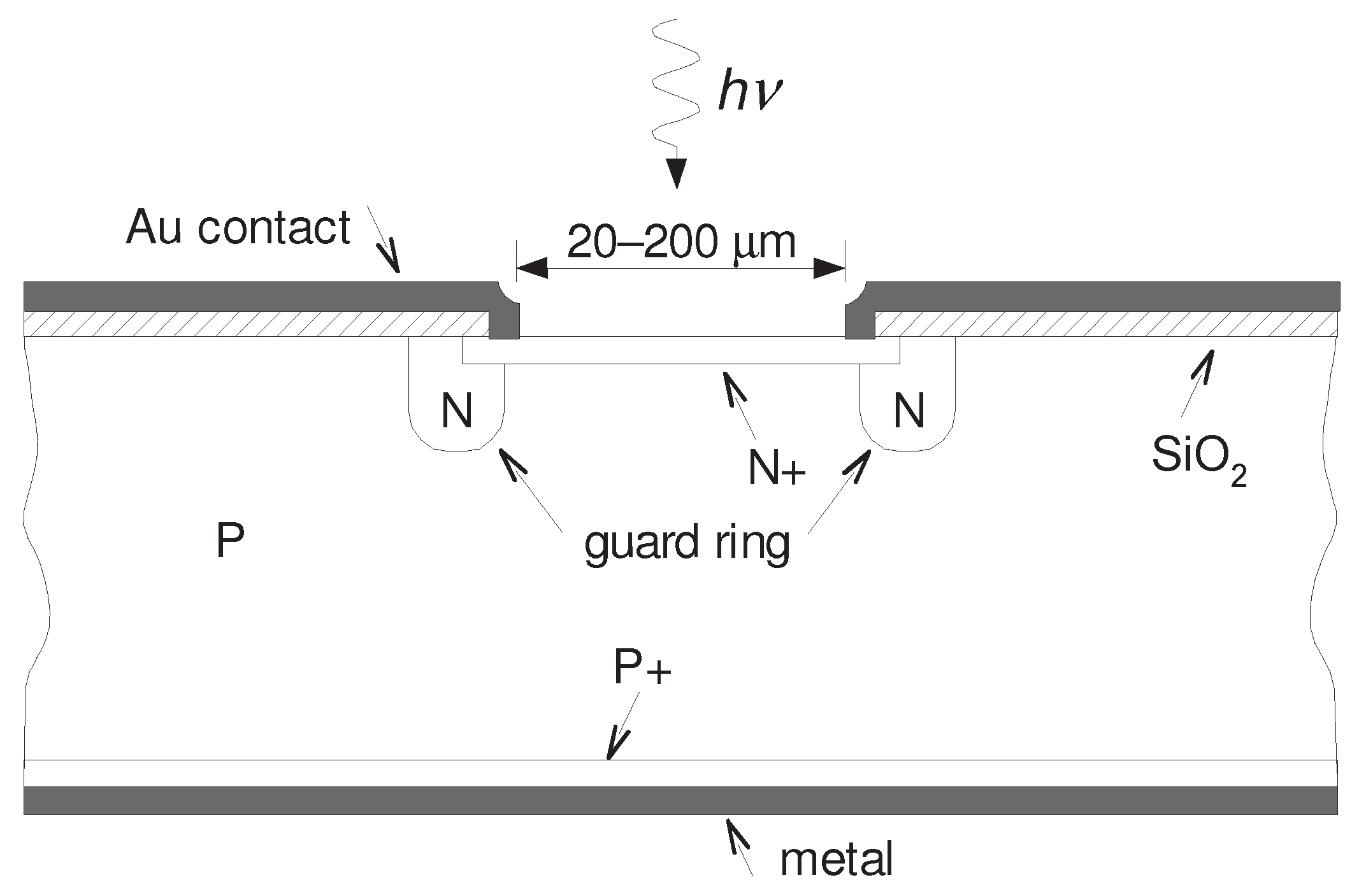
Figure 2.
Cross-section of the K14 SPAD structure. The silicon bulk is p-doped, typical thickness of whole structure is 500 µm.
Figure 2.
Cross-section of the K14 SPAD structure. The silicon bulk is p-doped, typical thickness of whole structure is 500 µm.
The SPAD sensor developed at Czech Technical University was manufactured by custom manufacturing process called K14, based on standard planar epitaxial technology [
6]. The structure of K14 diode is depicted in
Figure 2. The K14 diode is so-called thin SPAD pointing out that the depletion layer of p-n junction is thin, around 1 µm. Compared to thick SPADs (with depletion layer 20–150 µm), this results in better timing performance, low timing jitter and low breakdown voltage on order of tens of volts; about 28 V for K14. On the other hand, thin SPADs have reduced quantum efficiency due to lower volume where the photon can be absorbed [
6,
8].
There is a guard ring around the photon sensitive area made of n-type semiconductor reducing the danger of microplasma breakdown caused by steep gradient typical for SPAD sensors. Moreover, the guard ring restricts the multiplication area to specific region [
3]. There were manufactured K14 diodes with sensitive area of several diameters ranging from 20 µm to 200 µm with outstanding uniformity regardless of the sensitive area. The pictures of a K14 SPAD chip can be found in
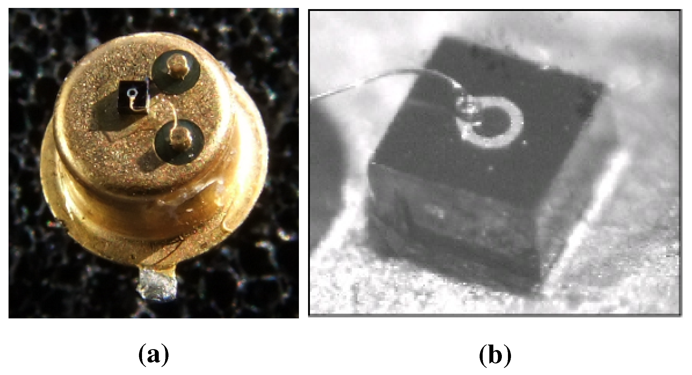
Figure 3.
Figure 3.
(
a) The picture of K14 SPAD chip mounted onto a standard TO (Transistor Outline) package. The anode is at the bottom of the chip mounted to the package via an electrical conductive adhesive [
9]; (
b) The detail of the chip active area diameter of 100 µm with wire bonding of the diode cathode. The sensitive area is inside the circle formed by cathode metal contact [
6].
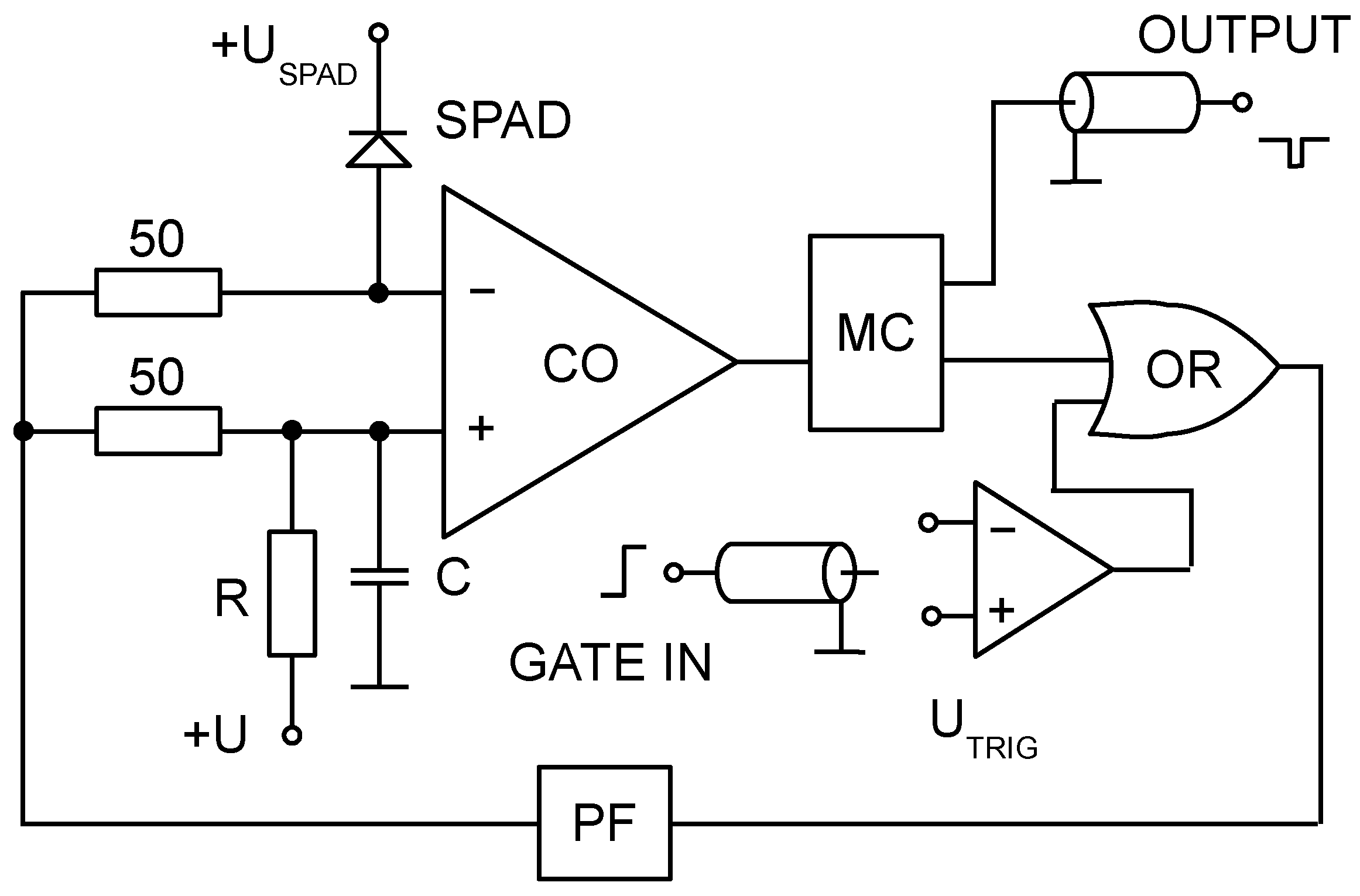
Figure 4.
Block diagram of active quenching and gating circuit [
10]. The reset (quenching) time of detector is determined mainly by a propagation delay of the comparator CO and the gate OR.
Figure 4.
Block diagram of active quenching and gating circuit [
10]. The reset (quenching) time of detector is determined mainly by a propagation delay of the comparator CO and the gate OR.
The K14 SPAD is operated coupled with a custom made active quenching and gating circuits inspired by Cova [
11]. These slightly vary according to target application in which the detector containing the K14 diode is used. A common block diagram of such a circuitry can be found in
Figure 4. The avalanche is sensed by a comparator (CO). The generated pulse is stretched by a monostable circuit and logically ORed with gate input. The output drives a pulse-forming circuit, output of which controls the bias on the SPAD.
Beside active quenching, also passive quenching may be employed. In such a circuit, there is a resistor in series with the diode. When a breakdown occurs, the current increase due to the avalanche causes increase of voltage at the resistor, hence, decrease of voltage at the diode, resulting in avalanche quenching. The advantage over active quenching is simplicity of the circuit. On the other hand, active quenching may be used at higher count rates [
8]. Not only because the quenching time is generally longer in passive case, but also because the passive circuit results in longer biasing time of thediode [
12].
2.2. Detector Properties
Several parameters of the K14 SPAD and its supporting electronics are described in following section. Especially parameters which are outstanding [
4] compared to other SPAD detectors are emphasized. The point of view on each parameter depends on intended application [
13]. The dark count noise of the K14 SPAD is relatively high, but for many space application with high background flux its importance is negligible. On the other hand, its stability of temporal response and uniformity of sensitivity within sensitive area allow few-photon recognition [
14] and multi-photon compensation [
15].
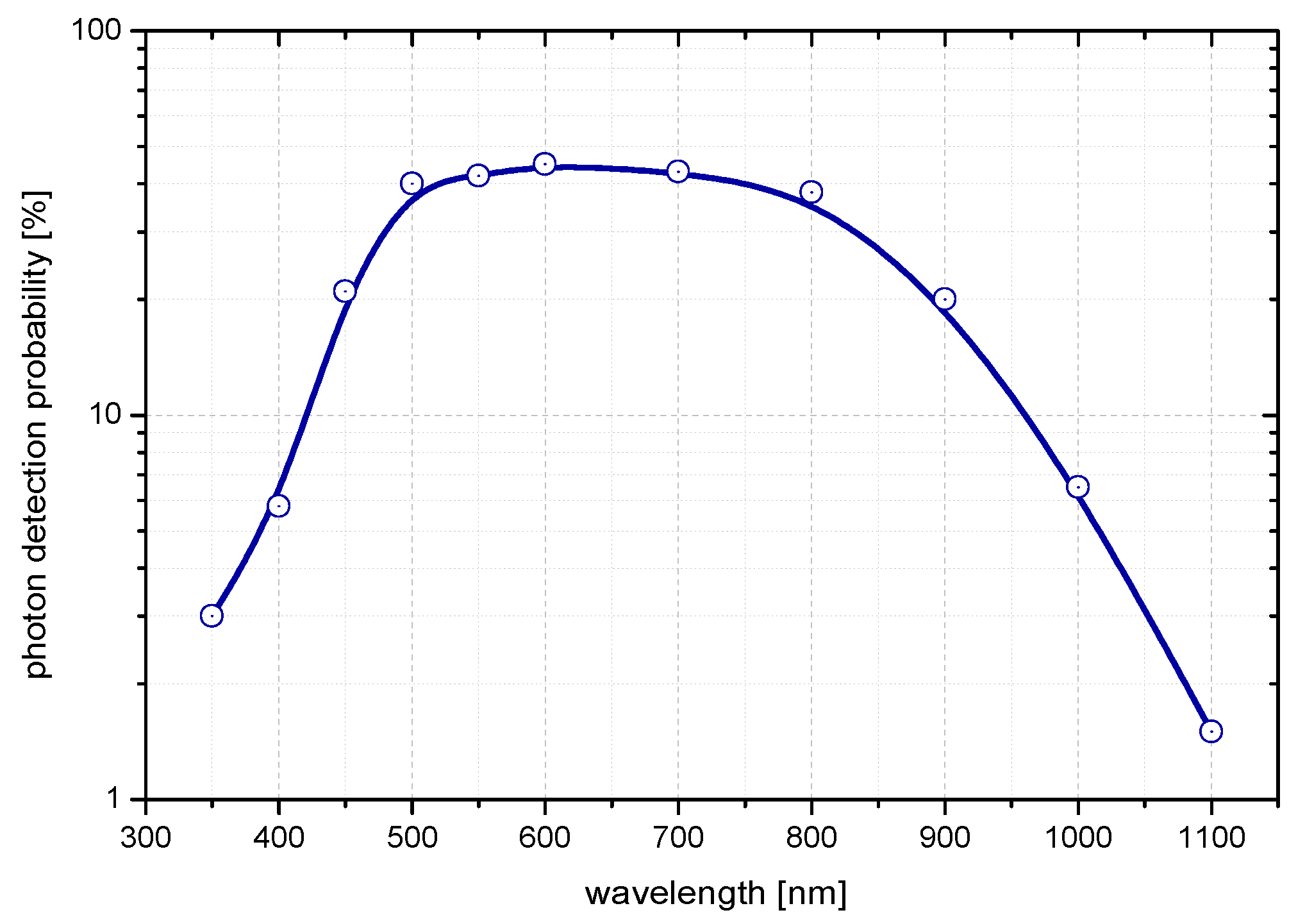
The K14 sensor spectral sensitivity with 1 V bias voltage at room temperature is depicted in
Figure 5 and is determined by its core material—silicon. Note that the detection probability is increased with increasing bias voltage and it is red-enhanced with increasing temperature of detector. It can be up to five times higher for 4 V bias above breakdown voltage. Selected bias voltage is always a deal between the detection probability, temporal resolution and dark count probability. All three factors are directly proportional to the bias voltage.
Figure 5.
Typical detection probability versus wavelength [
16] for a chip with a sensitive area of 20 µm and 1 V bias above breakdown voltage at room temperature.
Figure 5.
Typical detection probability versus wavelength [
16] for a chip with a sensitive area of 20 µm and 1 V bias above breakdown voltage at room temperature.
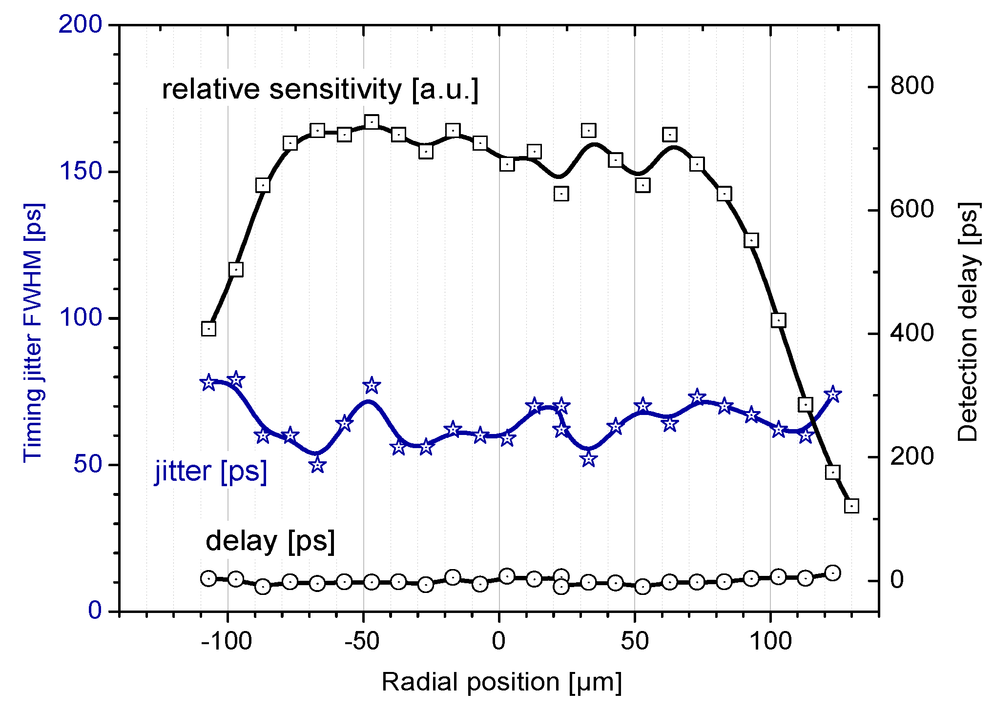
Figure 6.
Uniformity of a typical 200 µm K14 SPAD. Note the detection delay, independent on position of seed photoelectron. This uniformity is absolutely crucial property for any photon-number dependent application such as few-photon detection and multi-photon time-walk compensation. It is also necessary for application where exact position of incident photon is unpredictable, e.g. in focus of a large telescope.
One of the unique properties of the K14 SPAD is its uniformity. That means the detection delay remains the same regardless on the position in active area, in which the incident photon is absorbed. This maintains high temporal resolution and low jitter even for detectors with large sensitive area (200 µm) [
6]. An experiment was performed to verify the K14 uniformity [
6]. A light spot of size of few micrometers scanned the surface of active area by employing micrometer shifts with accuracy of few micrometers. Relative sensitivity, timing resolution and detection delay across the SPAD structure was measured at several points of the active area. The results are depicted in
Figure 6. Note that the data spread of the detection delay is caused by a statistical nature of the measured parameter.
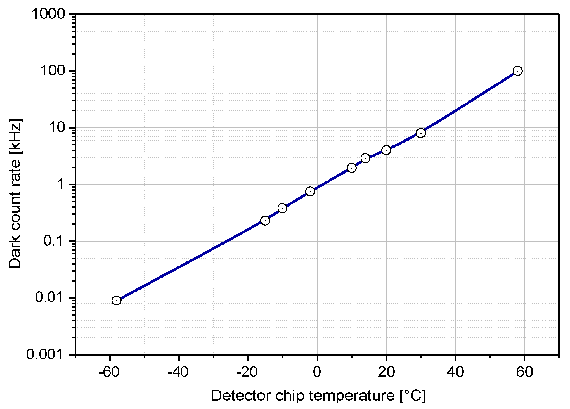
An electron–hole pair generation and avalanche establishment can occur after biasing of the SPAD even without the incident photon. This events are caused by lattice thermal vibrations together with crystal defects and impurities, and they are called dark counts. These cause false detections and determine the internal noise of the detector. The dark counts—thus the noise—can be diminished by cooling the sensor [
17]. Dependence of dark count on temperature of K14 diode is shown in
Figure 7.
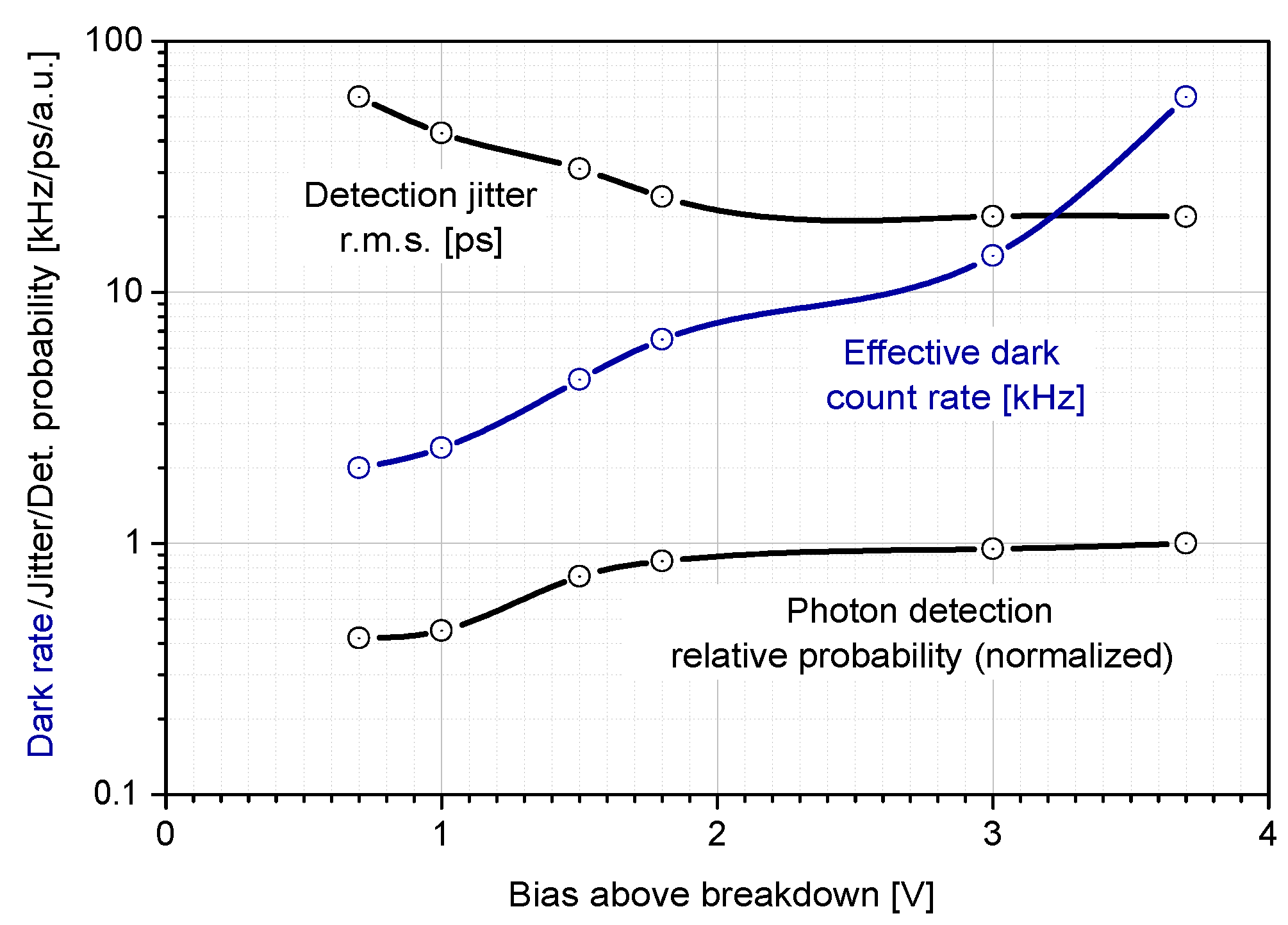
Most of the monitored properties of the K14 SPAD are dependent on the bias. Some properties (see below) are better with higher bias operation, some of them deteriorate. For this reason, the bias have to be carefully selected with respect to target application. Having in mind key detector properties for respective application, a trade-off is usually undertaken [
18]. Three important detector parameters—timing jitter, dark count rate, and detection probability—are plotted against the bias in
Figure 8. Note that with increasing bias, the detection probability and timing jitter is improved while the number of darkcounts increases.
Figure 7.
Dark count rate of the detector is strongly dependent on temperature of the structure. Depicted dependence is valid for typical K14 SPAD of 40 µm active area operated 0.7 V above breakdown voltage. Note the slope of one decade decrease of dark count rate per 30 K. The absolute value of dark count rate depends on bias, see
Figure 8.
Figure 8.
Three important and interconnected parameters of typical 200 µm K14 sensor cooled at −60 °C plotted against the bias voltage.
Figure 8.
Three important and interconnected parameters of typical 200 µm K14 sensor cooled at −60 °C plotted against the bias voltage.
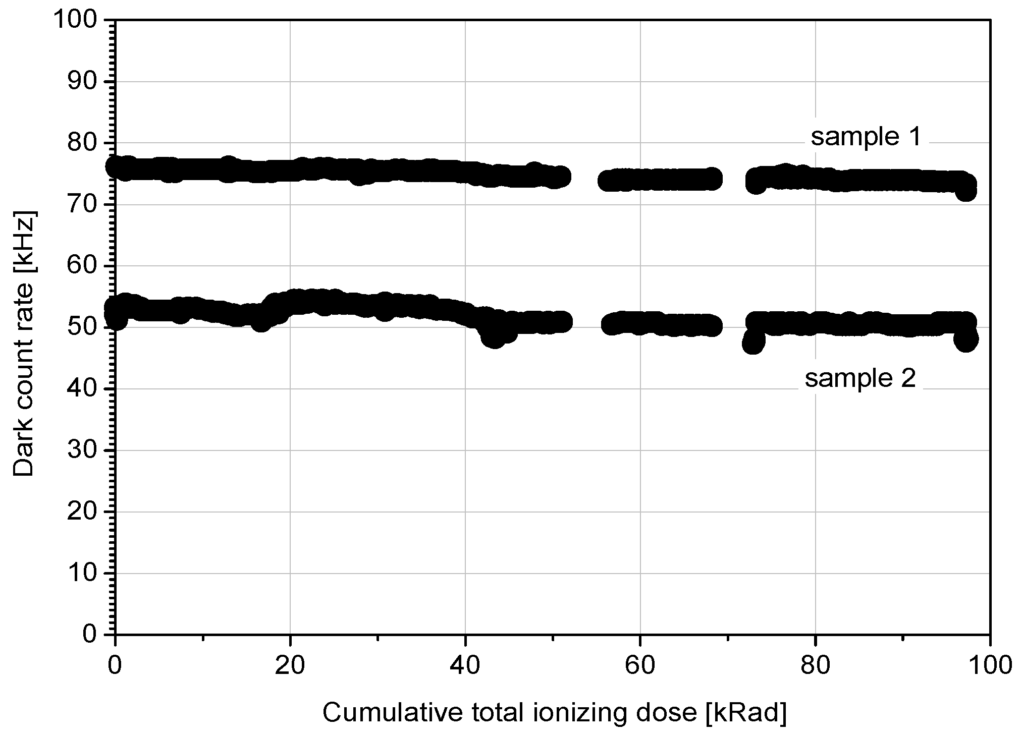
An important feature of the K14 sensor is its radiation hardness. This was verified during the years in three main tests. Moreover, the radiation hardness was proved in practice via in orbit operation onboard Jason-2 and COMPASS satellites. The terrestrial radiation tests were performed in three different laboratories. One of them were performed in CNES laboratory in Toulouse, France in frame of T2L2 project. The diodes underwent Total Ionizing Dose (TID) of 100 krad. The dark count rate of the detector operated in Geiger mode was recorded regularly as the dose grew, see
Figure 9.
Figure 9.
Dark count rate stability of two selected K14 100 µm diodes while irradiated. Note two different dark count rate values demonstrating variation in dark count rate sample by sample whereas it is independent on imposed radiation dose.
Figure 9.
Dark count rate stability of two selected K14 100 µm diodes while irradiated. Note two different dark count rate values demonstrating variation in dark count rate sample by sample whereas it is independent on imposed radiation dose.
Beside the dark count, timing resolution and sensitivity were monitored after the irradiation. In
Figure 10, these parameters are compared among irradiated and not irradiated samples of the diodes. The experiment has shown that the K14 SPAD is fairly radiation resistant and has no measurable change in monitored parameters—dark count rate, timing resolution, and sensitivity—after TID of 100 krad [
18].
Figure 10.
Timing resolution and sensitivity of reference (not irradiated samples) 1, 4, 5 and 100 krad irradiated samples 2, 3. The irradiated samples does not exhibit any measurable parameter change.
Figure 10.
Timing resolution and sensitivity of reference (not irradiated samples) 1, 4, 5 and 100 krad irradiated samples 2, 3. The irradiated samples does not exhibit any measurable parameter change.
Next radiation experiment was performed at Nuclear Research Institute in Řež, Czech Republic. A radiation source of
60Co was employed in a geometrical setup that results in radiation speed of 2.5 rad/s. The total irradiation time was 225 min resulting in TID of 34 krad. Similarly to above mentioned experiment, such a radiation dose did not degrade monitored parameters—timing jitter, dark count rate, and breakdown voltage. However, it must be noted that the present gamma radiation increase the effective dark count rate during the experiment as the gamma photons triggered the avalanche. The dark count rate increased from 0.2 MHz to 1.2 MHz. It dropped back to 0.2 MHz after the source of gamma radiation was shielded [
18].
Final radiation experiment with K14 SPADs were performed at Indiana University Cyclotron Facility in Bloomington, USA. In comparison with above mentioned experiments, a proton flux instead of gamma rays was employed as a radiation source. Various fluxes of 53 MeV protons struck the K14 diodes in several scenarios—diode operated in active quenching and gating circuit, diode under steady bias below breakdown voltage, and diode with shorted pins. In contrast to gamma radiation, proton flux caused significant deterioration (increase) of dark count rate due to displacement damage in the structure of the diode. This happened for much lower TID than used in previous gamma rays experiments. It was shown that the increase in dark count rate is not only dependent on TID but also on proton flux value. The higher value of proton flux, the higher increase in dark count rate was observed. The diodes exposed to proton fluxes of values in range of 10
4 cm
−2s
−1 to 2.3 × 10
8 cm
−2s
−1 exhibit increase of dark count rate on average from 0.27 MHz to 0.55 MHz at TID of 0.3 krad, 2.33 MHz at 3 krad, and 4.9 MHzat 6.65 krad [
19].
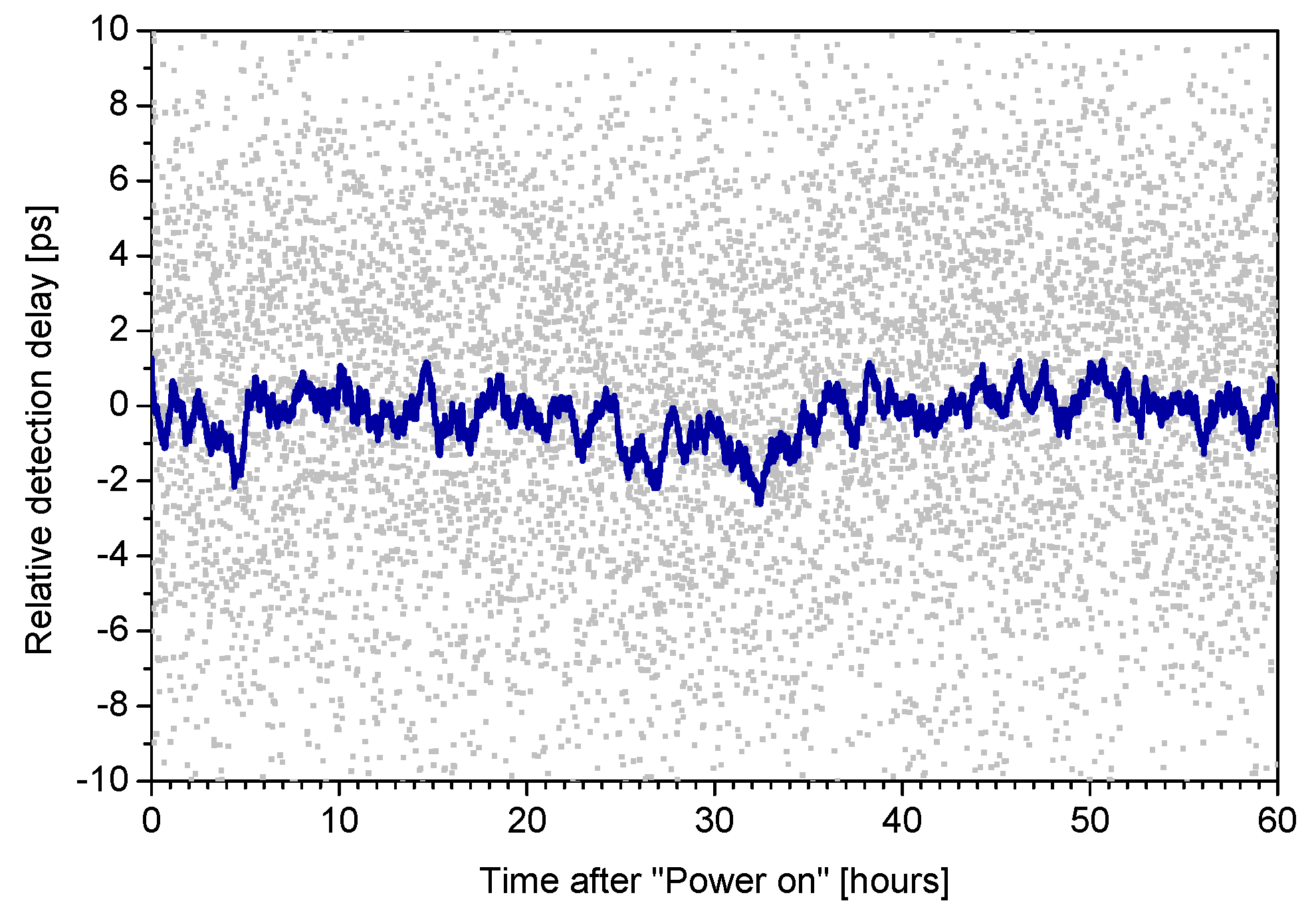
Figure 11.
The verification of detector stability. Detection delay readings averaged over 1000 s during a Time-Correlated Single Photon Counting (TCSPC) experiment [
20] in more than two days.
Figure 11.
The verification of detector stability. Detection delay readings averaged over 1000 s during a Time-Correlated Single Photon Counting (TCSPC) experiment [
20] in more than two days.
One of the most important key features of the K14 sensor and the detector electronics for intended applications is its detection delay stability. The stability was among others verified in a Time Correlated Single Photon Counting (TCSPC) experiment lasting more than 2 days. A short pulse (42 ps) laser diode of 778 nm wavelength and in house built NPET timing system (New Picosecond Event Timing device) with sub-picosecond resolution and great timing stability [
21] was employed. The results are depicted in
Figure 11 and
Figure 12.
Figure 11 shows delay detection measurements averaged over 1000 s. The delay remains within ±1 ps while the ambient temperature fluctuations during the experiment were within ±1 K.
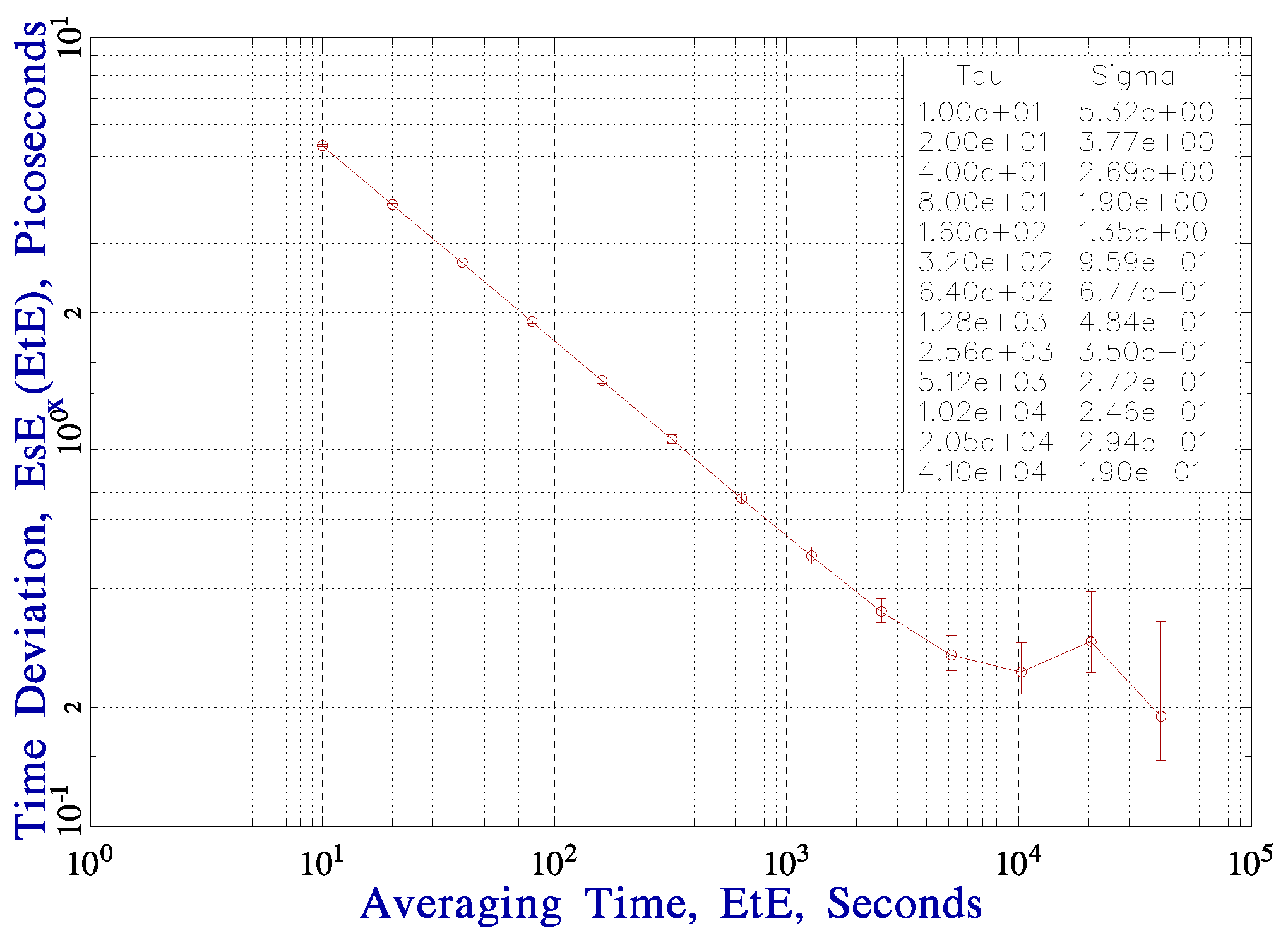
Figure 12 shows time deviation (TDEV) of the whole TCSPC experiment including stabilities of laser, start detector and NPET timing system. Note the plateau below 200 fs at averaging times of few hours. Same results were obtained for thermo-electrically cooled 200 µm chips as well as 100 µm chips without thermal management [
20].
Figure 12.
Time deviation of the entire TCSPC experiment [
20]. In the sense of TDEV the long-term detection stability is better than 200 fs after several hours. In other words, it is meaningful to process data collected in several hours acquisition.
Figure 12.
Time deviation of the entire TCSPC experiment [
20]. In the sense of TDEV the long-term detection stability is better than 200 fs after several hours. In other words, it is meaningful to process data collected in several hours acquisition.
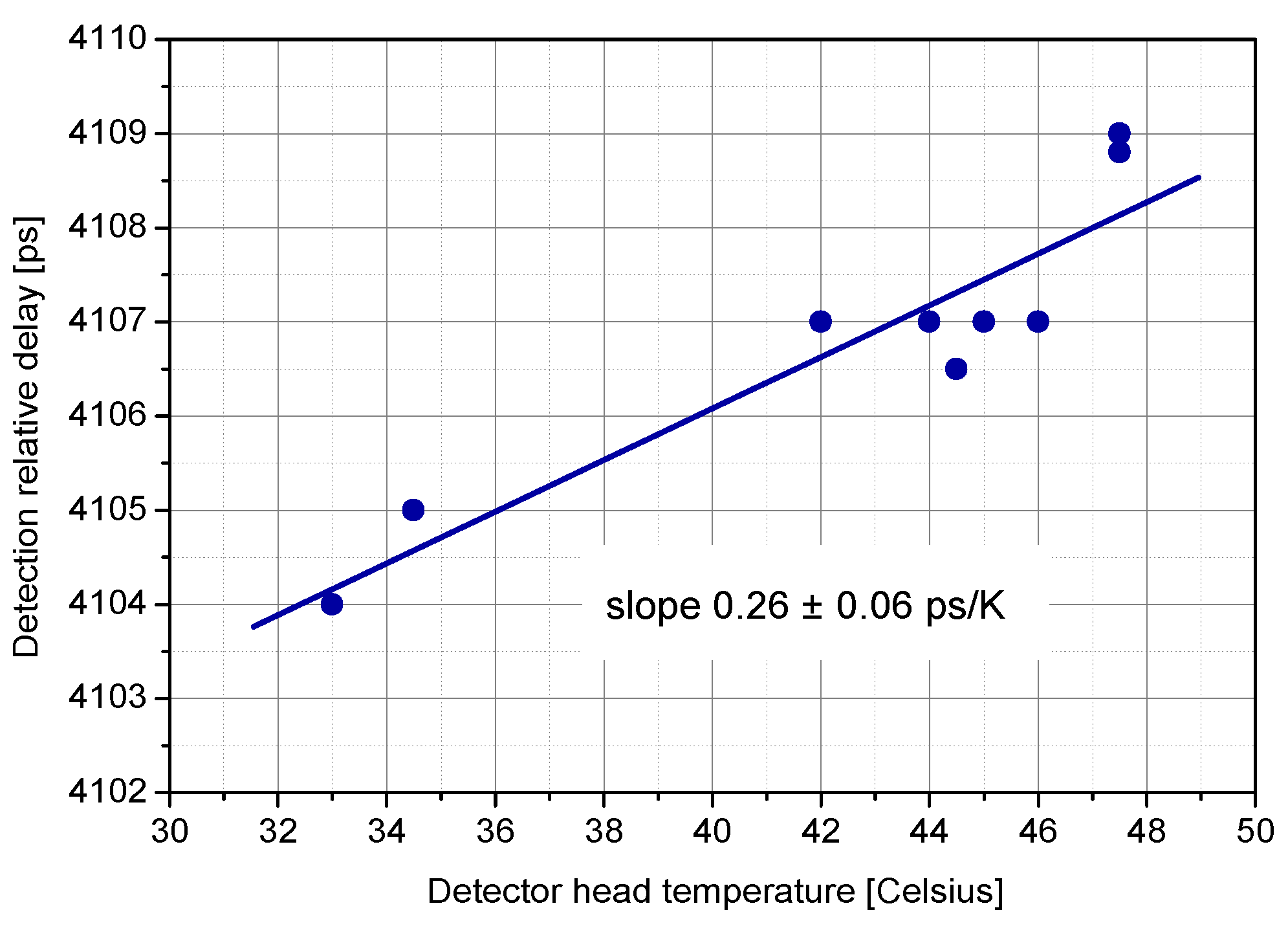
The detection delay stability is affected by mainly two influences, namely, temperature and the number of incident photons. The dependence of detection delay on temperature changes was measured in a TCSPC experiment with the result of 0.26 ps/K, see
Figure 13.
Figure 13.
Temperature dependence of detection delay [
20] for typical chip and active quenching circuit with the built-in temperature compensation.
Figure 13.
Temperature dependence of detection delay [
20] for typical chip and active quenching circuit with the built-in temperature compensation.
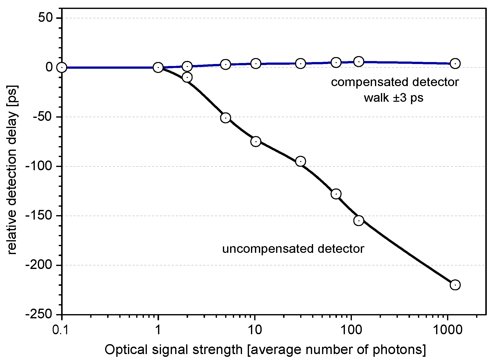
Another detection delay fluctuations are caused by varying optical input strength, thus incident number of photons. The degree of such an influence is dependent among others on voltage bias and pulse width in case of multiphoton level. The level of so called time walk is not acceptable for sub-centimeter Satellite Laser Ranging (SLR). For this reason, an effort in compensation of such an effect was made. It was shown that the rise time of avalanche pulse is slightly shorter for multiphoton level than for single photon level. This observation was employed by the SLR group in Graz to develop a time walk compensating circuit [
15]. The detection delay dependence on the number of incident photons of compensated and uncompensated K14 detector is shown in
Figure 14. Another way to mitigate the time walk caused by varying signal strength is to ensure the single-photon level at the detector input; this approach is used for instance in the European Laser Timing project [
22].
Figure 14.
Detection delay of compensated (C-SPAD) [
7] and uncompensated SPAD dependence on number of incident photons. The core of ground-segments of many photon-counting space projects.
Figure 14.
Detection delay of compensated (C-SPAD) [
7] and uncompensated SPAD dependence on number of incident photons. The core of ground-segments of many photon-counting space projects.
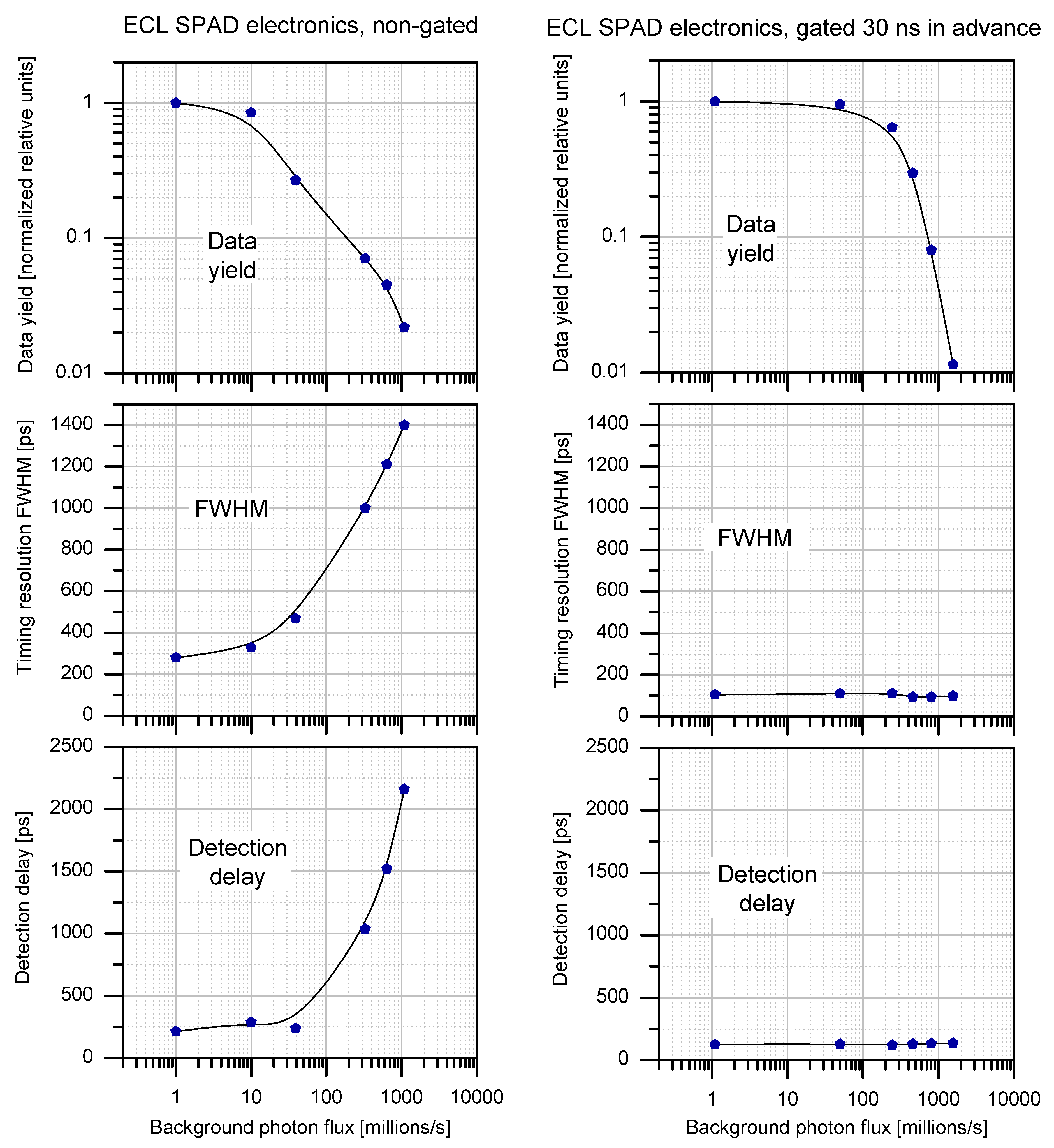
Note well the number of incident photons mentioned above means number of signal photons from the laser pulse concentrated in few tens of picosecond. On the other hand, the detection delay is fairly stable under various background photon flux in range of 1 to several million photons per second when operated in gated mode.


