
Amorphous Silicon p-i-n Structure Acting as Light and Temperature Sensor


Abstract
:1. Introduction
2. Material and Methods
Fabrication Process of the Device
- Cleaning of the glass substrate:
- ultrasonic cleaning in Detergent 8 (by Alconox) diluted at 5% in deionized water (DI) for 30 min;
- ultrasonic rinse in DI at 50 °C for 15 min;
- ultrasonic cleaning in Liquinox (by Alconox) diluted at 2% in DI for 30 min;
- ultrasonic rinse in DI at 50 °C for 15 min;
- drying in nitrogen flow; and
- immediately positioning of the glass substrate inside the RF magnetron sputtering system.
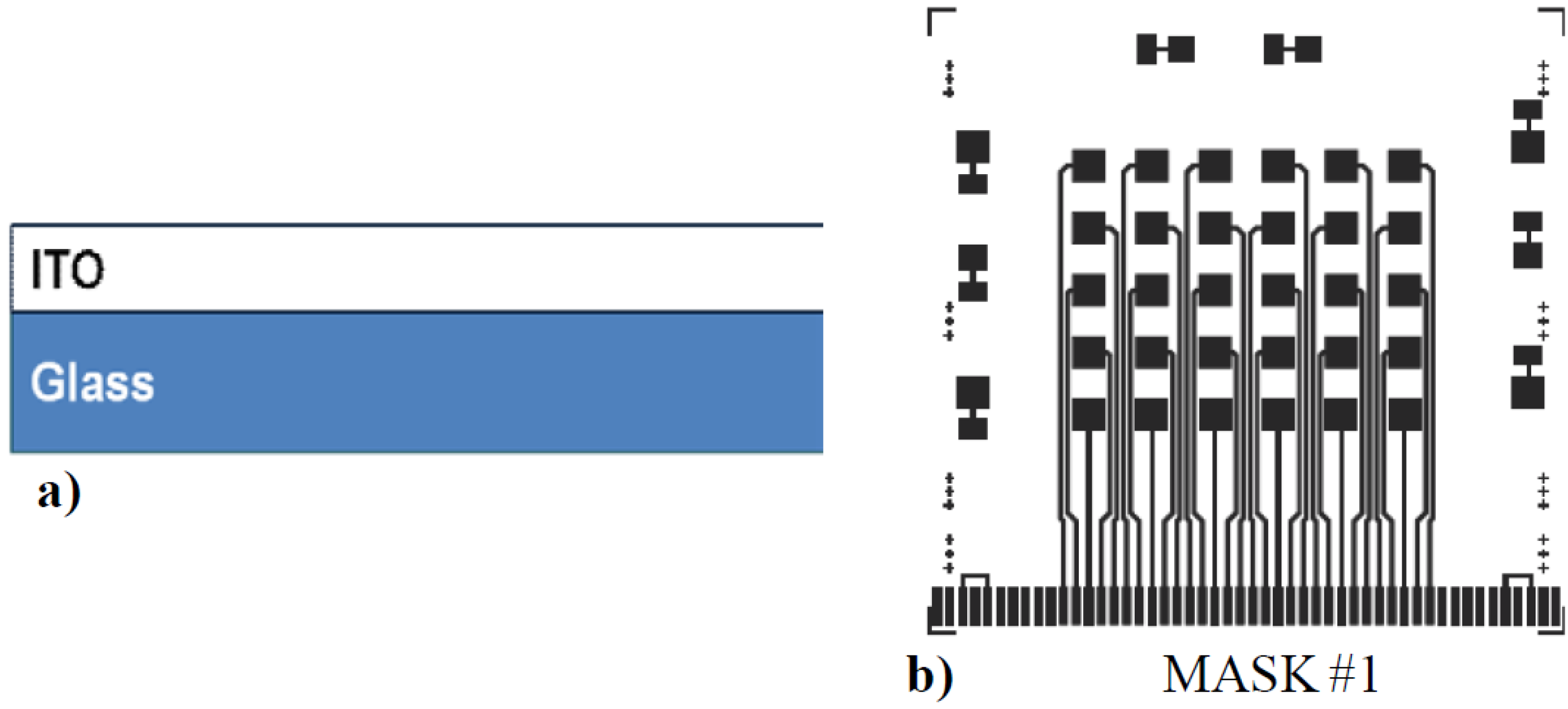
- Sputter deposition (in Material Research Corporation system) of 200 nm thick layers from a 6-in-diameter Indium Tin Oxide (ITO) target (with 90% In2O3–10% SnO2 in weight composition), at 200 W of RF power, 2.7 mTorr of pressure process, 25 sccm of argon flow and 120 °C substrate temperature (Figure 1a).
- First lithographic step:
- spin coating of photoresist (AZ1518 from Shipley);
- soft bake at 100 °C for 1 min;
- UV exposure through a lithographic mask at 320 mJ/cm2 for 45 s; and
- development of the photoresist in AZ351B diluted at 25% in DI for 45 s.
- Patterning of ITO layer (with mask #1 in Figure 1b) by Sputter Etching at 180 W, 50 sccm Argon flow and 90 mTorr.Figure 1. (a) Structure of the sensor after step 4 of the fabrication process. (b) Photolithographic mask used for the patterning of ITO bottom electrode of the device.Figure 1. (a) Structure of the sensor after step 4 of the fabrication process. (b) Photolithographic mask used for the patterning of ITO bottom electrode of the device.
![Sensors 15 12260 g001]()
- Covering the ITO markers with kapton tape to allow the subsequent alignments.
- Sequential deposition, by Plasma Enhanced Chemical Vapor Deposition (PECVD) in a three UHV chamber system, of the hydrogenated p-type a-SiC, intrinsic and n-type a-Si layers, that constitute the stacked structure of the diode. The following Table 1 reports the deposition parameters of the PECVD process.Table 1. PECVD parameters used in the deposition of the a-Si:H and a-SiC:H layers. The gases are: SiH4 pure silane, PH3 silane diluted (5%), B2H6 helium diluted (5%), CH4 pure methane; PD is the process pressure; PRF is the power density of the plasma discharge; TD is the substrate temperature; tD is the deposition time. The thicknesses reported above have been estimated from the growth rate of the different materials.
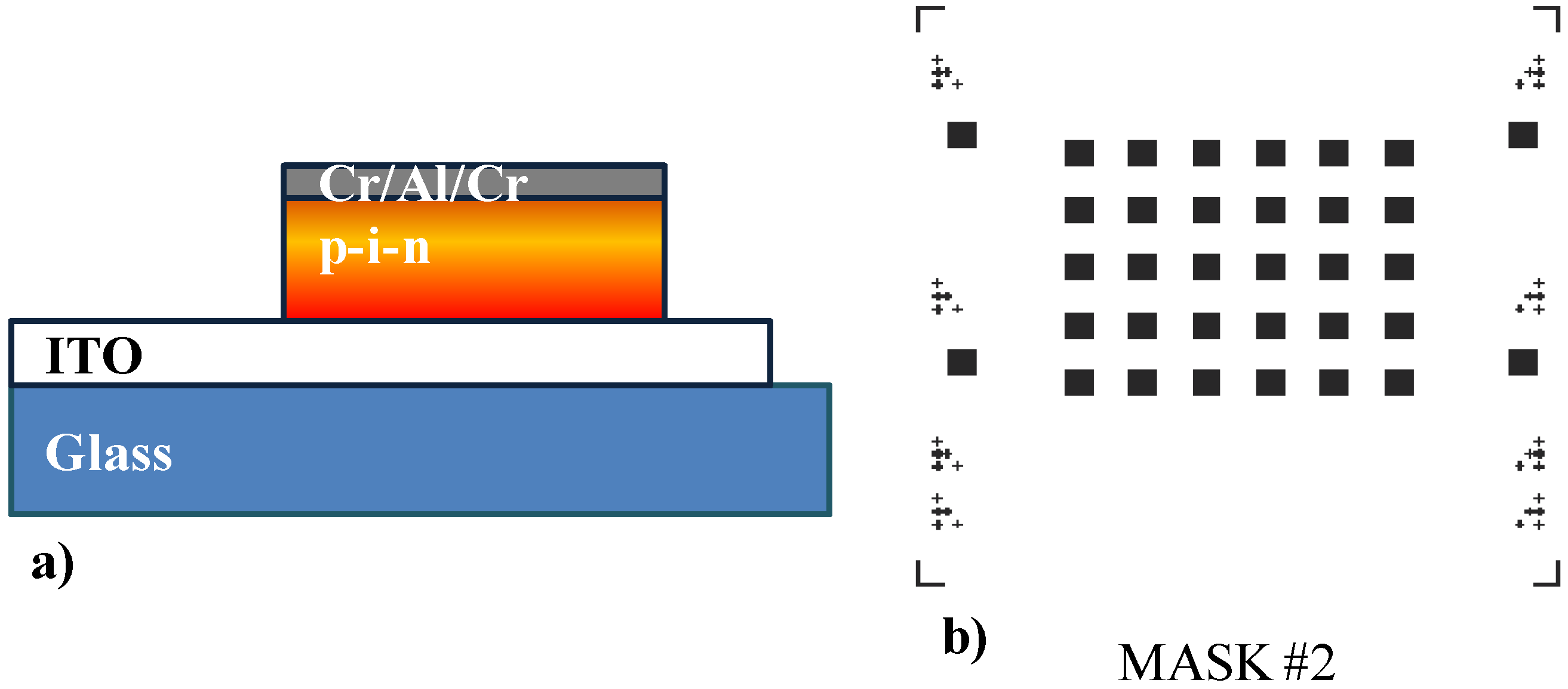
Table 1. PECVD parameters used in the deposition of the a-Si:H and a-SiC:H layers. The gases are: SiH4 pure silane, PH3 silane diluted (5%), B2H6 helium diluted (5%), CH4 pure methane; PD is the process pressure; PRF is the power density of the plasma discharge; TD is the substrate temperature; tD is the deposition time. The thicknesses reported above have been estimated from the growth rate of the different materials. Layer type/material SiH4 (sccm) PH3 (sccm) B2H6 (sccm) CH4 (sccm) PD (Torr) PRF (mW/cm2) TD (°C) tD (sec) Thickness (nm) p/a-SiC:H 40 5 60 0.7 25 150 60 10 i/a-Si:H 40 0.68 25 180 2100 400 n/a-Si:H 40 10 0.3 25 200 180 50 - Deposition of a three metal layer stack of Cr/Al/Cr with thickness of 30/200/30 nm, respectively, in an Ultra Vacuum system (thermal evaporator by Balzers) with measured growth rate of 0.3 nm for Cromium and 1 nm for Aluminum.
- Peeling of the kapton tape, for the subsequent alignments.
- Lithographic steps (see point 3) with Mask #2 in Figure 2b.
- Patterning of the Cr layer by wet etching in a solution of 30 g Ce(NH4)2(NO3)6, 9 mL CH3COOH and 200 mL DI for 1 min.
- Patterning of the Aluminum layer by wet etching in a solution of 80 mL H3PO4 (85%), 5 mL HNO3 and 10 mL DI.
- Patterning of the Cr layer by wet etching (see point 10).
- Patterning of the a-Si:H n-i-p structure by dry etching in a Reactive Ion Etching system (by IONVAC) (Figure 2a) with the following parameters:
- Oxigen (O2) flow O2: 10 sccm;
- Carbon tetrafluoride (CF4) flow: 100 sccm; and
- Radio Frequency Power Density: 300 mW/cm2.
Figure 2. (a) Structure of the sensor after the step 13 of the fabrication process. (b) Photolithographic mask used for the patterning of the mesa structure of the device.Figure 2. (a) Structure of the sensor after the step 13 of the fabrication process. (b) Photolithographic mask used for the patterning of the mesa structure of the device.![Sensors 15 12260 g002]()
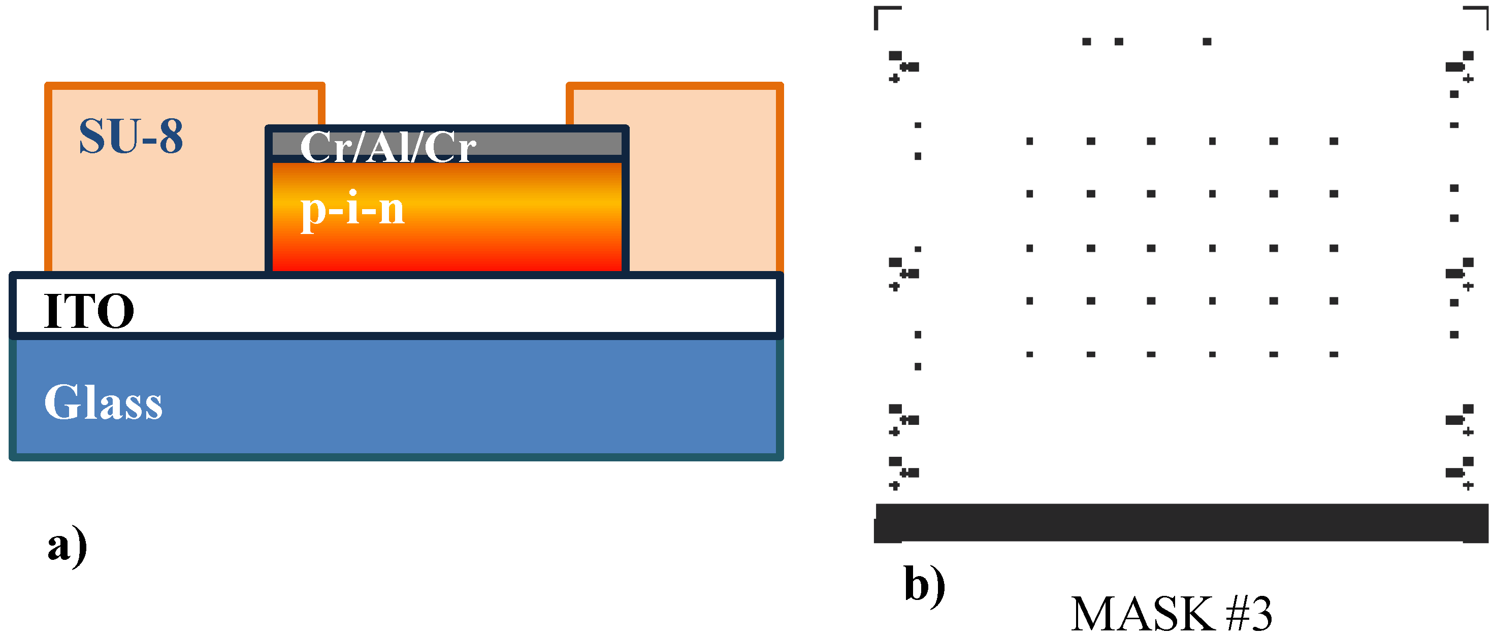
- Deposition by spin coating of a 5 µm-thick SU8 (from Micro-Chem, MA, USA) and its pattering through Mask #3 in Figure 3b for opening via holes over the diodes (Figure 3a). The deposition of the SU-8 film is implemented through the following steps:
- spin coating at 500 rpm for 5 s followed by another run at 3000 rpm for 30 s;
- bake at 65 °C for 1 min followed by another bake at 95 °C for 2 min;
- UV-light exposition at 250 mJ/cm2;
- bake at 65 °C for 1 min followed by another bake at 95 °C for 1 min;
- developing in SU-8 remover;
- rinse in isopropyl alcool; and
- hard bake at 150 °C for 30 min.
Figure 3. (a) Structure of the sensor after step 14 of the fabrication process. (b) Photolithographic mask used for the patterning of the via on the SU8 insulation layer.Figure 3. (a) Structure of the sensor after step 14 of the fabrication process. (b) Photolithographic mask used for the patterning of the via on the SU8 insulation layer.![Sensors 15 12260 g003]()
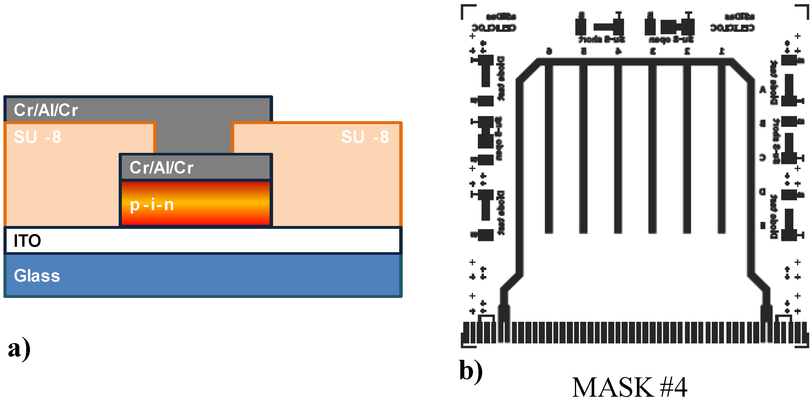
- Deposition of a three metal layer stack of Cr/Al/Cr with thickness of 30/200/30 nm, respectively, in an Ultra Vacuum system (see point 7).
- Lithographic steps (see point 3) with Mask #4 in Figure 4b.
- Patterning of the Cr/Al/Cr layers (see points 10 an 11).Figure 4. (a) Structure of the sensor after step 17 of the fabrication process; (b) Photolithographic mask used for the patterning of the metallic lines for the electrical connection of the top electrode of the device to the edge of the glass substrate.Figure 4. (a) Structure of the sensor after step 17 of the fabrication process; (b) Photolithographic mask used for the patterning of the metallic lines for the electrical connection of the top electrode of the device to the edge of the glass substrate.
![Sensors 15 12260 g004]()
- Deposition by spin coating of a 5 µm-thick SU-8 as passivation layer and hard baking at 150 °C for 30 min.

3. Structure and Characterization of the Device
3.1. Sensor Structure
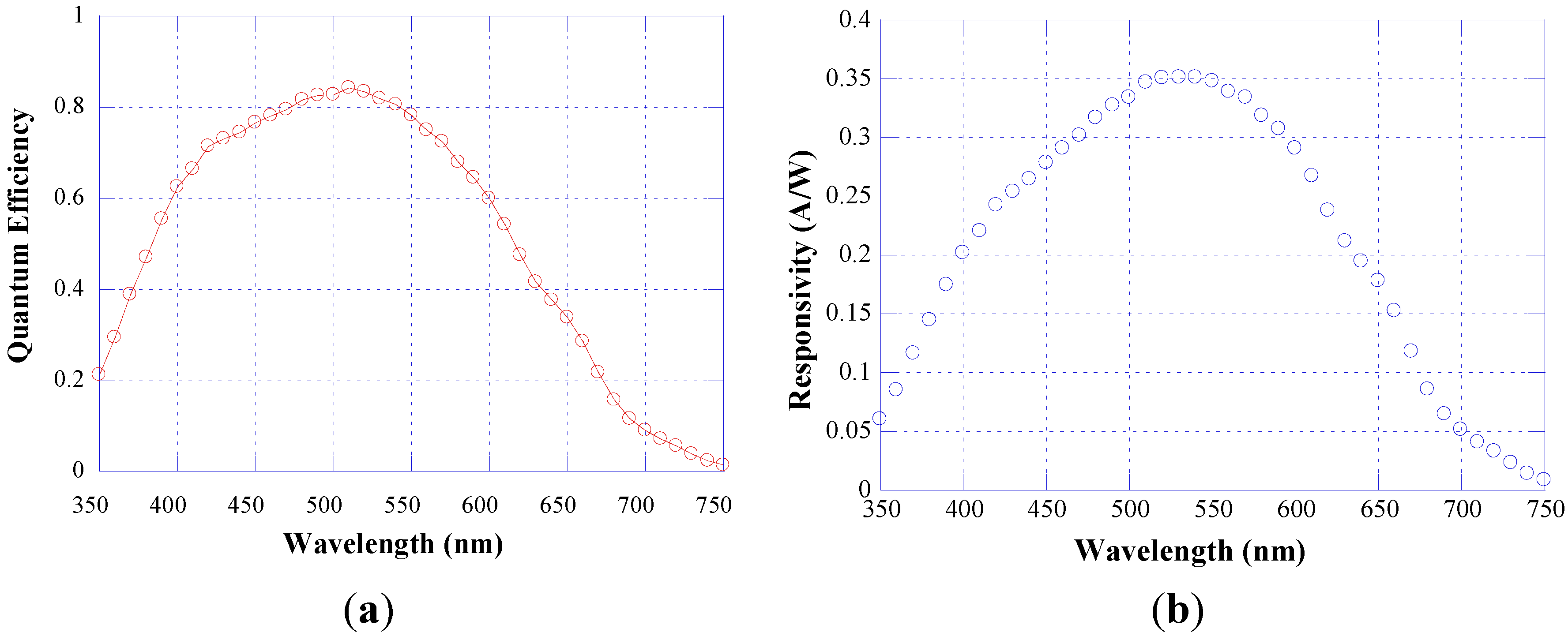
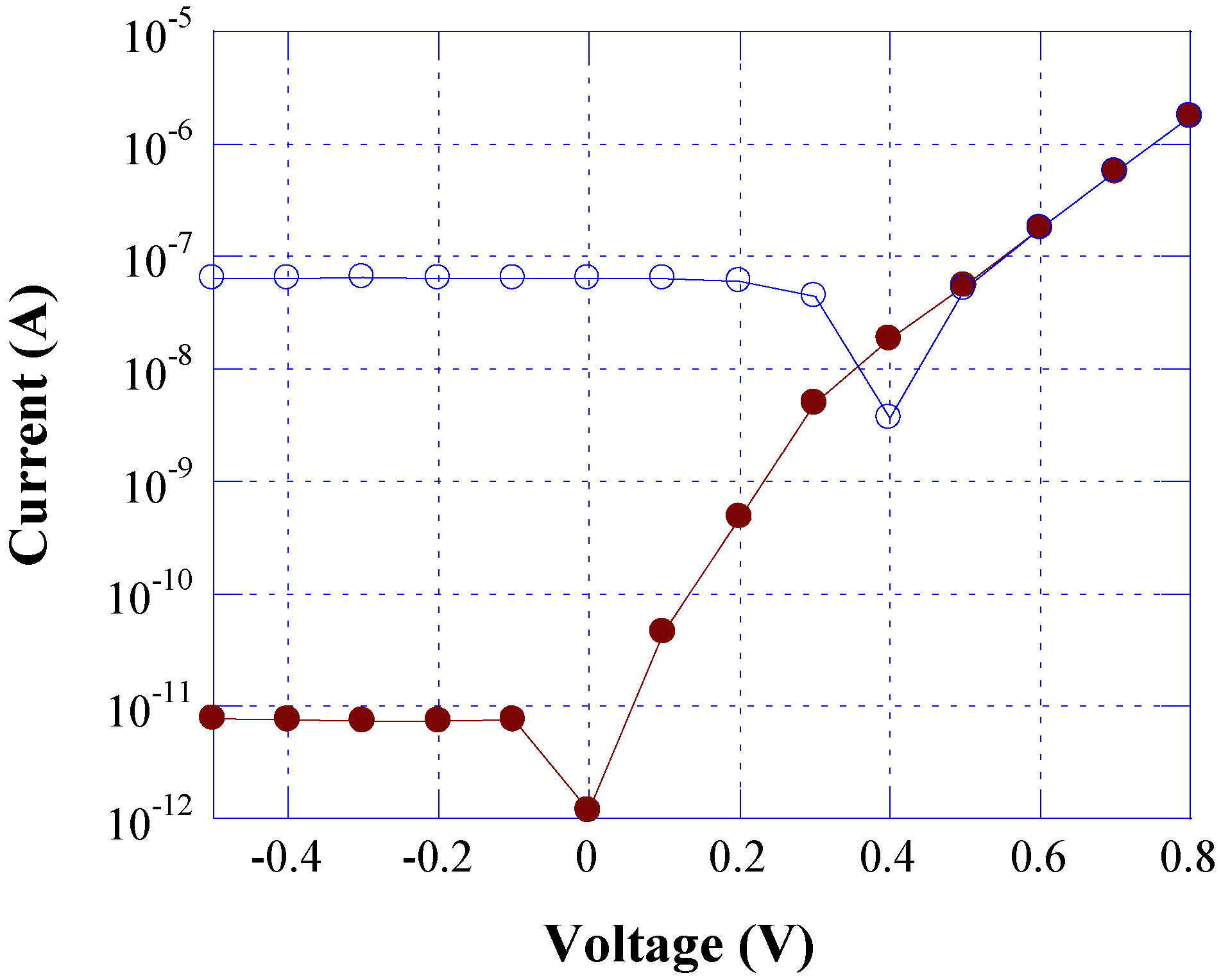
3.2. Characterization as Radiation Sensor
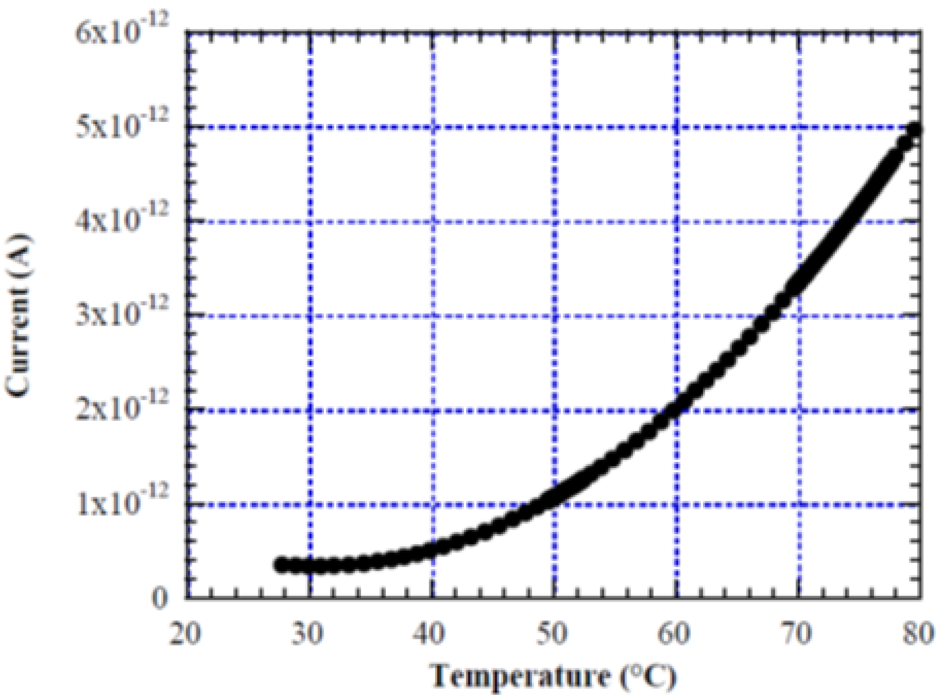
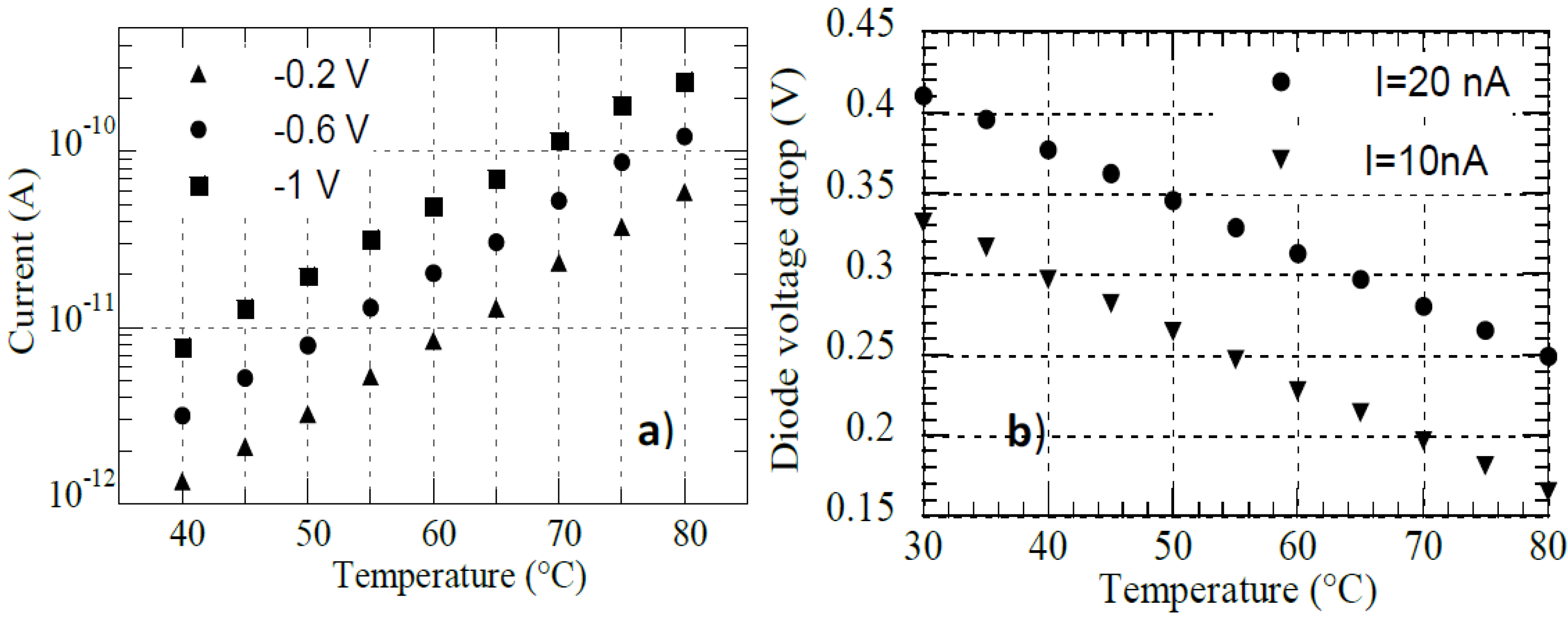
3.3. Characterization as Temperature Sensor
4. Results and Discussion
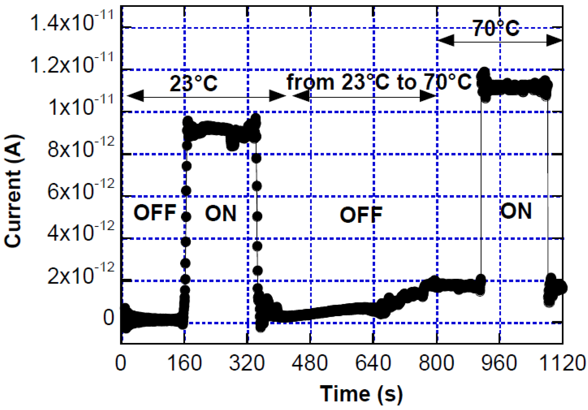
4.1. Temperature Effect on Light Measurement

4.2. Effect of Light Intensity on Temperature Measurement
5. Conclusions
Acknowledgments
Author Contributions
Conflicts of Interest
References
- Manz, A.; Graber, N.; Widmer, H.M. Miniaturized total Chemical Analysis systems: A Novel Concept for Chemical Sensing. Sens. Actuators B Chem. 1990, 1, 244–248. [Google Scholar] [CrossRef]
- Rabner, A.; Shacham, Y. A Concept for a Sensitive Micro Total Analysis System for High Throughput Fluorescence Imaging. Sensors 2006, 6, 341–349. [Google Scholar] [CrossRef]
- Caputo, D.; de Cesare, G.; Scipinotti, R.; Mirasoli, M.; Roda, A.; Zangheri, M.; Nascetti, A. Chemiluminescence-Based Micro-Total-Analysis System with Amorphous Silicon Photodiodes. Lect. Notes Electr. Eng. 2014, 268, 207–211. [Google Scholar]
- Guiducci, C.; Stagni, C.; Fischetti, A.; Mastromatteo, U.; Benini, L.; Riccò, B. Microelectrodes on a Silicon Chip for Label-Free Capacitive DNA Sensing. IEEE Sensors J. 2006, 6, 1084–1093. [Google Scholar] [CrossRef]
- Waleed Shinwari, M.; Zhitomirsk, D.; Deen, I.A.; Selvaganapathy, P.R.; Jamal Deen, M.; Landheer, D. Microfabricated Reference Electrodes and their Biosensing Applications. Sensors 2010, 10, 1679–1715. [Google Scholar] [CrossRef] [PubMed]
- Miled, M.A.; Sawan, M. Dielectrophoresis-Based Integrated Lab-on-Chip for Nano and Micro-Particles Manipulation and Capacitive Detection. IEEE Trans. Biomed. Circuits Syst. 2012, 6, 120–132. [Google Scholar] [CrossRef] [PubMed]
- Lee, T.M.H.; Carles, M.C.; Hsing, I.M. Microfabricated PCR-electrochemical device for simultaneous DNA amplfication and detection. Lab Chip 2003, 3, 100–105. [Google Scholar] [CrossRef] [PubMed]
- Medoro, G.; Nastruzzi, C.; Guerrieri, R.; Gambari, R.; Manaresi, N. Lab on a Chip for Live-Cell Manipulation. IEEE Des. Test 2007, 24, 26–36. [Google Scholar] [CrossRef]
- Caputo, D.; de Cesare, G.; Dolci, L.S.; Mirasoli, M.; Nascetti, A.; Roda, A.; Scipinotti, R. Microfluidic chip with integrated a-Si:H photodiodes for chemiluminescence-based bioassays. IEEE Sens. J. 2013, 13, 2595–2602. [Google Scholar] [CrossRef]
- Dutse, S.W.; Yusof, N.A. Microfluidics-Based Lab-on-Chip Systems in DNA-Based Biosensing: An Overview. Sensors 2011, 11, 5754–5768. [Google Scholar] [CrossRef] [PubMed]
- Bahşi, Z.B.; Büyükaksoy, A.; Ölmezcan, S.M.; Şimşek, F.; Aslan, M.H.; Oral, A.Y. A Novel Label-Free Optical Biosensor Using Synthetic Oligonucleotides from E.Coli O157:H7: Elementary Sensitivity Tests. Sensors 2009, 9, 4890–4900. [Google Scholar] [CrossRef] [PubMed]
- Jha, S.K.; Joo, G.-S.; Ra, G.-S.; Lee, H.H.; Kim, Y.-S. Development of PCR Microchip for Early Cancer Risk Prediction. IEEE Sens. J. 2011, 11, 2065–2070. [Google Scholar] [CrossRef]
- Wu, J.; Cao, W.; Wen, W.; Chang, D.C.; Sheng, P. Polydimethylsiloxane microfluidic chip with integrated microheater and thermal sensor. Biomicrofluidics 2009, 3. [Google Scholar] [CrossRef] [PubMed]
- Matos Pires, N.M.; Dong, T.; Hanke, U.; Hoivik, N. Recent Developments in Optical Detection Technologies in Lab-on-a-Chip Devices for Biosensing Applications. Sensors 2014, 14, 15458–15479. [Google Scholar] [CrossRef] [PubMed]
- Hofmann, O.; Miller, P.; Sullivan, P.; Jones, T.S.; deMello, J.C.; Bradley, D.D.C.; deMello, A.J. Thin-film organic photodiodes as integrated detectors for microscale chemiluminescence assays. Sens. Actuators B Chem. 2005, 106, 878–884. [Google Scholar]
- Wang, X.; Amatatogchai, M.; Nacaprocha, D.; Hofmann, O.; de Mello, J.C.; Bradley, D.D.C.; de Mello, A.J. Thin-film organic photodiodes for integrated on-chip chemilunescence detection – application to antioxidant capacity screening. Sens. Actuators B Chem. 2009, 140, 643–648. [Google Scholar] [CrossRef]
- Matos Pires, N.M.; Dong, T.; Hanke, U.; Hoivik, N. Integrated optical microfluidic biosensor using a polycarbazole photodetector for point-of-care detection of hormonal compounds. J. Biomed. Opt. 2003, 18. [Google Scholar] [CrossRef]
- Liu, C.-H.; Chang, Y.-C.; Norris, T.B.; Zhong, Z. Graphene photodetectors with ultra broadband and high responsivity at room temperature. Nat. Nanotechnol. 2014, 9, 273–278. [Google Scholar] [CrossRef] [PubMed]
- Carlson, D.E. Amorphous silicon solar cells. IEEE Trans. Electron Devices 1977, ED-24, 449–453. [Google Scholar] [CrossRef]
- Caputo, D.; de Cesare, G. New a-Si:H Two Terminal Switching Device for Active Display. J. Non-Cryst. Solids 1996, 198–200, 1134–1137. [Google Scholar] [CrossRef]
- Ibaraki, N. a-Si TFT technologies for AM-LCDs. MRS Proc. 1994. [Google Scholar] [CrossRef]
- De Cesare, G.; Gavesi, M.; Palma, F.; Riccò, B. A novel a-si:H mechanical stress sensor. Thin Solid Films 2003, 427, 191–195. [Google Scholar] [CrossRef]
- Caputo, D.; de Cesare, G.; Nascetti, A.; Tucci, M. Detailed study of amorphous silicon ultraviolet sensor with chromium silicide window layer. IEEE Trans. Electr. Dev. 2008, 55, 452–456. [Google Scholar] [CrossRef]
- Schaefer, H.; Seibel, K.; Walder, M.; Schoeler, L.; Pletzer, T.; Waidelich, M.; Ihmels, H.; Ehrhardt, D.; Boehm, M. Monolithic integrated optical detection for microfluidic systems using thin film photodiodes based on amorphous silicon. In Proceedings of the 18th IEEE International Conference on Micro Electro Mechanical Systems, Miami, FL, USA, 30 January–3 February 2005; pp. 758–761.
- Costantini, F.; Nascetti, A.; Scipinotti, R.; Domenici, F.; Sennato, S.; Gazza, L.; Bordi, F.; Pogna, N.; Manetti, C.; Caputo, D.; et al. On-chip detection of multiple serum antibodies against epitopes of celiac disease by an array of amorphous silicon sensors. RSC Adv. 2014, 4, 2073–2080. [Google Scholar] [CrossRef]
- Kamei, T.; Toriello, N.M.; Lagally, E.T.; Blazej, R.G.; Scherer, J.R.; Street, R.A.; Mathies, R.A. Microfluidic Genetic Analysis with an Integrated a-Si:H Detector. J. Biomed. Microdevices 2005, 7, 147–152. [Google Scholar] [CrossRef] [PubMed]
- Martins, R.; Baptista, P.; Raniero, L.; Doria, G.; Silva, L.; Franco, R.; Fortunato, E. Amorphous/nanocrystalline silicon biosensor for the specific identification of unamplified nucleic acid sequences using gold nanoparticle probes. Appl. Phys. Lett. 2007, 90. 023903–1/023903–3. [Google Scholar] [CrossRef]
- Pimentel, A.C.; Pereira, A.T.; Chu, V.; Prazeres, D.M.F.; Conde, J.P. Detection of chemiluminescence using an amorphous silicon photodiode. IEEE Sens. J. 2007, 7, 415–416. [Google Scholar] [CrossRef]
- Joskowiak, A.; Chu, V.; Prazeres, D.M.F.; Conde, J.P. Amorphous Silicon Photosensors for Detection of Intrinsic Cell Fluorophores. MRS Proc. 2011, 1321, 435–439. [Google Scholar] [CrossRef]
- Caputo, D.; de Cesare, G.; Fanelli, C.; Nascetti, A.; Ricelli, A.; Scipinotti, R. Amorphous silicon photosensors for detection of Ochratoxin A in wine. IEEE Sens. J. 2012, 12, 2674–2679. [Google Scholar] [CrossRef]
- Caputo, D.; de Cesare, G.; Nascetti, A.; Negri, R. Spectral tuned amorphous silicon p-i-n for DNA detection. J. Non-Cryst. Solids 2006, 352, 2004–2006. [Google Scholar] [CrossRef]
- Caputo, D.; de Cesare, G.; Fanelli, C.; Nascetti, A.; Ricelli, A.; Scipinotti, R. Innovative detection system of ochratoxin A by thin film photodiodes. Sensors 2007, 7, 1317–1322. [Google Scholar] [CrossRef]
- Gibbs, R.A. DNA Amplification by the Polymerase Chain Reaction. Anal. Chem. 1990, 62, 1202–1214. [Google Scholar] [CrossRef] [PubMed]
- Zhang, C.; Xu, J.; Ma, W.; Zheng, W. PCR microfluidic devices for DNA amplification. Biotechnol. Adv. 2006, 24, 243–284. [Google Scholar] [CrossRef] [PubMed]
- Caputo, D.; de Cesare, G.; Nardini, M.; Nascetti, A.; Scipinotti, R. Monitoring of temperature distribution in a thin film heater by an array of a-Si:H temperature sensors. IEEE Sens. J. 2012, 12, 1209–1213. [Google Scholar] [CrossRef]
- De Cesare, G.; Caputo, D.; Tucci, M. Electrical properties of ITO/crystalline silicon contact at different deposition temperatures. IEEE Electron Devices Lett. 2012, 33, 327–329. [Google Scholar] [CrossRef]
- Street, R.A. Large Area Image Sensor Array. In Technology and Applications of Amorphous Silicon; Springer-Verlag: Berlin, Germany, 2000; Chapter 4; p. 151. [Google Scholar]
- Ibañez, G.A.; Escandar, G.M. Luminescence Sensors Applied to Water Analysis of Organic Pollutants—An Update. Sensors 2011, 11, 11081–11102. [Google Scholar] [CrossRef] [PubMed]
- Caputo, D.; de Cesare, G.; Nascetti, A.; Negri, R.; Scipinotti, R. Amorphous Silicon Sensors for Single and Multicolor Detection of Biomolecules. IEEE Sens. J. 2007, 7, 1274–1280. [Google Scholar] [CrossRef]
- Caputo, D.; de Cesare, G.; Scipinotti, R.; Stasio, N.; Costantini, F.; Manetti, C. On Chip Diagnosis of Celiac Disease by an Amorphous Silicon Chemiluminescence Detector. Lect. Notes Electr. Eng. 2014, 268, 183–187. [Google Scholar]
- Schiff, E.A.; Street, R.A.; Weisfield, W. Reverse bias currents in amorphous silicon nip sensors. J. Non-Cryst. Solids 1996, 198–200, 1155–1159. [Google Scholar] [CrossRef]
- Sze, S.M. p-n Junction Diode. In Physics of Semiconductor Device, 2nd ed.; John Wiley and Sons: Hoboken, NJ, USA, 1981; Chapter 2; pp. 84–94. [Google Scholar]
- Forward Bias Characteristics of 1N400x Family Diodes. Available online: http://www.cliftonlaboratories.com/1n400x_diode_family_forward_voltage.htm (accessed on 25 May 2015).
© 2015 by the authors; licensee MDPI, Basel, Switzerland. This article is an open access article distributed under the terms and conditions of the Creative Commons Attribution license (http://creativecommons.org/licenses/by/4.0/).
Share and Cite
De Cesare, G.; Nascetti, A.; Caputo, D. Amorphous Silicon p-i-n Structure Acting as Light and Temperature Sensor. Sensors 2015, 15, 12260-12272. https://doi.org/10.3390/s150612260
De Cesare G, Nascetti A, Caputo D. Amorphous Silicon p-i-n Structure Acting as Light and Temperature Sensor. Sensors. 2015; 15(6):12260-12272. https://doi.org/10.3390/s150612260
Chicago/Turabian StyleDe Cesare, Giampiero, Augusto Nascetti, and Domenico Caputo. 2015. "Amorphous Silicon p-i-n Structure Acting as Light and Temperature Sensor" Sensors 15, no. 6: 12260-12272. https://doi.org/10.3390/s150612260
APA StyleDe Cesare, G., Nascetti, A., & Caputo, D. (2015). Amorphous Silicon p-i-n Structure Acting as Light and Temperature Sensor. Sensors, 15(6), 12260-12272. https://doi.org/10.3390/s150612260